Unit-2
Bipolar Junction Transistor
Q1) A 5.0V stabilized power supply is required to be produced from a 12V DC power supply input source. The maximum power rating PZ of the zener diode is 2W. Using the zener regulator circuit above calculate:
A1) a). The maximum current flowing through the zener diode.
Maximum current = Watts/ Voltage =2W/5V =400mA
b). The minimum value of the series resistor, RS
 = 17.5 Ω
c). The load current IL if a load resistor of 1kΩ is connected across the zener diode.

d). The zener current IZ at full load.
Iz =Is -Il =440mA – 5mA = 395mA
Q2) What would you expect to see displayed on oscilloscope connected across RL in the Limiter.

A2) The diode is forward biased and conducts when then the i/pvtg goes below -0.7v so for the –ve limiter , the peak o/p vtg across RL can be determined by the following
Volt=(RL/R+RL) Vin
=(1k/100+1k)10v
= 1K/1.1K*10
=1*103/1.1*103*10
= 1*104/11*102*10
= 1*104*10-2*10
=10/11 10*10*10/11
Volt=10000/11=9.09V
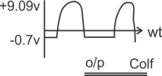
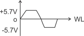
Q3) Fig shows a ckt combing a positive clipper with a-ve clipper. Determine the o/p vtg c/f

A3) When the voltage at point A riches +5.7V diode A conducted and limits the waveform to +5.7v diode D2 does not conduct until the voltage reaches -5.7V
Therefore positive voltages above +5.7V & -ve voltages below -5.7V are clipped off
Q4) Explain operation of positive and negative clamper in detail.
A4) 1) Positive Clamper:-
Diagram:-

Assumptions:-
1) The V/p is a perfect sine waveform
2)The value of R& C are chosen such that the Line constant T=RC is large equal
3)The diode is an ideal one
4)TheRc time constant is much longer as compared to one cattle period ‘T’ of the input.
RC>100T
Operation :-I n the first negative half cycle after turning on the Ckt the diode acts as a closed S/W & charges the capacitor to peak ilpvtg VM with the polarity shown below

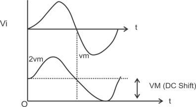
The diode reverse biased in both half cycle so it remains off.
2)Negative Clamper:-

In the first positive half cycle the capacitor will charge through the forward biased to peak vtgvm
The charging takes place very quickly as the diode resistances negligibly small
Once the capacitor charges to vm the diode is reverse biased and stops conducting.

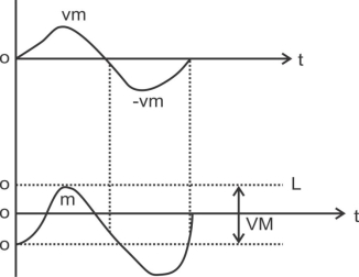
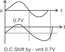
Diagram non ideal diode
Q5) An amplifier has a signal i/p Vtg. Vi of 0.25v and draws 1mA from the source. The amɤ delivers & v to a load at 10 mA. Determine the current Vtg and power gains. Also find the i/p resistance of this ampɤ what must be the open ckt. Vtg of the source Vs to provide an ampɤ i/p VtgVi of 0.25 v when the internal resistance of the source is 50 Ω?
A5) Given Vi = 0.25v, Ii = 1 Ma, Vo = 8 v, Io = 10 mA, Rs = 50 Ω.
Solution:
Vtg gain Av = 
Current gain =
= 
Power gain AP = Av  = 32
= 32 
Input resistance Ri =  = 250
= 250
Open circuit Vtg of Vs
Vi = 
Vs = 
Vs = 
Vs = 0.3v
Q6) Explain Common Base transistor in detail.
A6) The notation and symbols of pnp and npn transistors are given below:
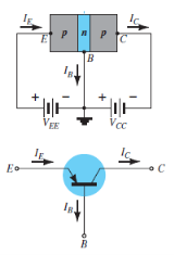
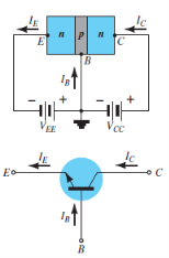
Fig.: PNP CB and NPN CB (Ref. 2)
Where Ic, Ib, Ie are the collector, base and emitter currents respectively.
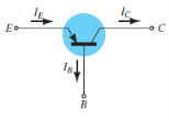
Fig. : PNP common base(Ref. 2)
Input Characteristic Curve
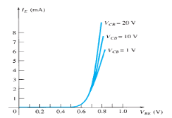
Fig.: Input Characteristic Curve (Ref. 2)
Output Characteristic Curve
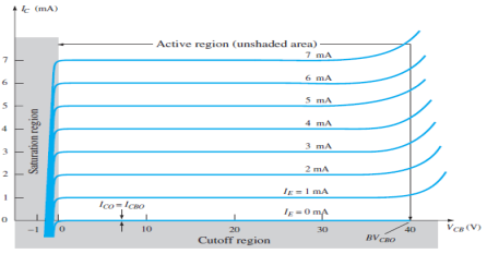
Fig.: Output Characteristic Curve (Ref. 2)
IC ≈ IE
2. Cut-off Region
3. Saturation Region
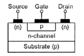
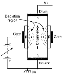
Q7) Explain JFET Operations in detail.
A7)
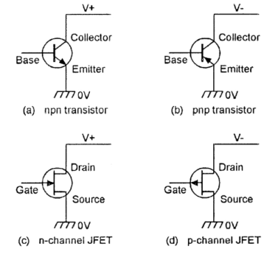
Operation
Q8) Draw and explain I-V characteristics.
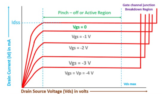
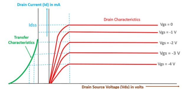
A8) Output Characteristics or Drain Characteristics
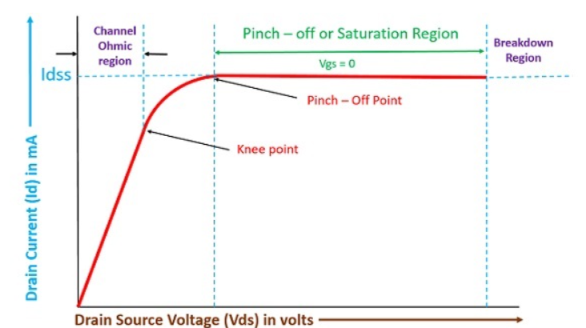
2. With external bias: When the external bias is applied to the gate-source terminal, the gate-source terminal becomes reversed bias externally. Obviously, if we are supplying an external voltage, then we can achieve the pinch-off point quite early as compared to the circuit which is not biased.
Transfer Characteristics
The transfer characteristics can be determined by observing different values of drain current with variation in gate-source voltage provided that the drain-source voltage should be constant. The transfer characteristics are just opposite to drain characteristics.
Q9) Explain MOSFET Operation in detail.
A9)
Operation
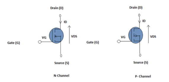
The MOSFET works by electronically varying the width of a channel along which charge carriers flow (electrons or holes).
The charge carriers enter the channel through source and exit via the drain.
The width of the channel is controlled by the gate voltage which is located between source and drain.
It is insulated from the channel near an extremely thin layer of metal oxide.
Function:
When there is no voltage on the gate, the channel shows maximum conductance. When the voltage on the gate is either positive or negative, the channel conductivity decreases.
2. Enhancement Mode
The device does not conduct when there is no voltage on the gate. As the voltage increases on the gate, the better the device can conduct.
Q10) Draw MOSFET Characteristics.
A10) MOSFET is seen to exhibit three operating regions viz.,
Cut-off region is a region in which the MOSFET will be OFF as there will be no current flow through it. In this region, MOSFET behaves like an open switch and is thus used when they are required to function as electronic switches.
Ohmic or linear region is a region where in the current IDS increases with an increase in the value of VDS. When MOSFETs are made to operate in this region, they can be used as amplifiers.
In saturation region, the MOSFETs have their IDS constant inspite of an increase in VDS and occurs once VDS exceeds the value of pinch-off voltage VP. Under this condition, the device will act like a closed switch through which a saturated value of IDS flows. As a result, this operating region is chosen whenever MOSFETs are required to perform switching operations.
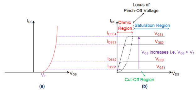
Fig: (a) Transfer Characteristics (b) Output Characteristics of NMOS
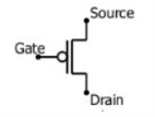
Q11) Explain NMOS and PMOS.
NMOS
NMOS is built on a p-type substrate with n-type source and drain diffused on it. Here, the majority carriers are electrons. When a high voltage is applied to the gate, the NMOS conducts and when low voltage is applied to the gate, it does not conduct. NMOS is faster than PMOS, as the carriers are electrons that travel twice as fast as the holes.
PMOS
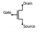
P-MOS consists of P-type Source and Drain diffused on an N-type substrate. Here, majority carriers are holes. When a high voltage is applied to the gate, the PMOS does not conduct and when a low voltage is applied, it conducts. These devices are more immune to noise than NMOS devices.
