MP
Unit-5Peripheral Devices Q1) Explain functional block diagram of 8237?A1) Functional block diagram:
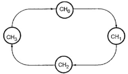
Fig 1 Functional Block Diagram of 8237The 8237 supplies memory & I/O with control signals and memory address information during the DMA transfer. It is actually a special-purpose microprocessor which transfer high-speed data between memory and I/O. 8237 is not a discrete component in modern microprocessor-based systems. It appears within many system controller chip sets. 8237 is a four-channel device compatible with 8086/8088, adequate for small systems. Expandable to any number of DMA channel inputs 8237 is capable of DMA transfers at rates up to 1.6MB per second. Each channel is capable of addressing a full 64K-byte section of memory. Q2) Explain operating modes of 8237?A2) The operating modes of 8237 are as follows:Rotating priority mode Here, the priority of channels has a circular sequence. The channel that is serviced has the lowest priority and the channel present next to it has the highest priority. This is explained with the help of figure.
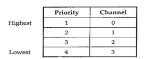
Fixed priority mode Here, channel 0 has highest priority and channel 3 has the lowest priority. After one channel is recognized for service, other channels are prevented from interfering until the service is completed.
Extended write mode It is used to provide alternate timing for the I/O or memory to write signals. This allows the devices to an early READY signal and prevents the unnecessary occurrence of wait states. It is done by activating MEMW and IOW signals . TC stop mode If TC is set, channel is disabled. Hence, it prevents further DMA operation on that channel. To enable DMA operation it is necessary to set the enable bit of the channel present in the mode set register. If TC stop bit is not set then the presence of TC output has no effect on the channel enable bits. Auto load mode When turned ON , it enables block chaining operations. In this, channel 2 parameters are initialized for the first data block. They are automatically copied to channel 3 registers. When an update cycle is initialized, the channel 3 parameters are transferred to channel 2. This is auto reload and is used for applications like CRT refreshing. Q3) Explain BSR mode of 8255?A3) The Bit Set/Reset (BSR) mode is available on port C only. Each and every line of port C (PC7 - PC0) can be set or reset by providing a suitable value to the control word register. BSR mode is independent and its selection does not affect the operation of other ports in I/O mode.
D7 bit is always 0 for this mode. Bits D6, D5 and D4 are don't care bits. Bits D3, D2 and D1 are used for pin selection of Port C. Bit D0 is used to set/reset the above selected pin. Selection of port C pin is determined as follows:
For example:If PC4 be set, then in the control word is, Since it is a BSR mode, D7 = '0'. Since D4, D5, D6 are don’t care hence assuming them to be '0'. PC4 has to be selected, hence, D3 = '1', D2 = '0', D1 = '0'. PC4 has to be set, hence, D0 = '1'. Thus, as per the above values, 0AH (in hex) will be loaded into the Control Word Register (CWR).Q4) Explain the operating modes of 8253?A4) 8253 can be operated in 6 different modes. They are:Mode 0 ─ Interrupt on Terminal Count It is used for generating an interrupt to the microprocessor after a certain interval. The output is low after the mode is set and remains LOW after the count value is loaded into the counter. The counter decrement continues till the terminal count is reached. The GATE signal remains high for normal counting. When it is low, counting is terminated and the current count is latched till it goes high again. Mode 1 – Programmable One Shot It is used as a mono stable multi-vibrator. GATE is used as a trigger input in this mode. As the count is loaded the output remains high and a trigger is applied. Mode 2 – Rate Generator The output is high after initialization. Whenever the count becomes zero, a low pulse is generated at the output and the counter is reloaded. Mode 3 – Square Wave Generator This mode is same as Mode 2 except that the output remains low for half of the timer period and high for the next half of the period. Mode 4 − Software Triggered Mode In this, the output remains high till the timer counts to zero and at this point the output is low and then goes high again. The count is latched when GATE LOW. As per the terminal count, for one clock cycle the output goes low then goes HIGH. The low pulse is used as a strobe. Mode 5 – Hardware Triggered Mode This mode generates a strobe as a result to an externally generated signal. It is same as mode 4 except that the counting is initiated by a signal at the gate input. As soon as it is initialized, the output goes high. When the terminal count is reached, the output goes low for one clock cycle. Q5) Explain the control word register of 8253/8254?A5) This register can be accessed when lines A0 & A1 are at logic 1. It is used to write a command word, its mode and either a read or write operation. Following table provides the result for various control inputs:
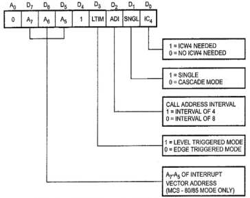
Q6) Write the control word for 8259?A6) Control word (ICW1):
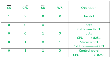
A write command issued to the 8259 with A0 = 0 and D4 = 1 is interpreted as ICW1, which starts the initialization sequence. It specifies,Single or multiple 8259As in the system 4 or 8 bit interval between the interrupt vector locations. The address bits A7 – A5 of the CALL instruction. (3 bits of lower byte address of CALL are given by user, rest bits are inserted by 8259A) Edge triggered or level triggered interrupts. ICW4 is needed or not. Q7) Explain R/W logic control of 8251?A7) Read/Write control logic –
It is a control block for overall device. It controls the overall working by selecting the operation to be done. The operation selection depends upon input signals as:
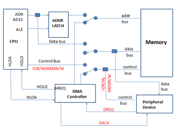
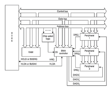
In this way, this unit selects one of the three registers- data buffer register, control register, status register.Q8) Explain handshaking in RS232?A8) Before the actual data transfer, signals are transmitted from DTE to DCE in order to make connections by a process known as handshaking. Following is the sequence of signal handshaking:Initially, the computer activates RTS signal to modem when a data is transferred from computer to modem. Modem in turn activates the DCD and then the CTS gets activated. Computer then sends data on TXD. After the data transmission is completed, the computer deactivates the RTS which causes the modem to deactivate CTS. Q9) Draw the interfacing diagram of 8237 with 8086?A9)
Q10) Draw block diagram of PIC and explain each block? A10) Block Diagram
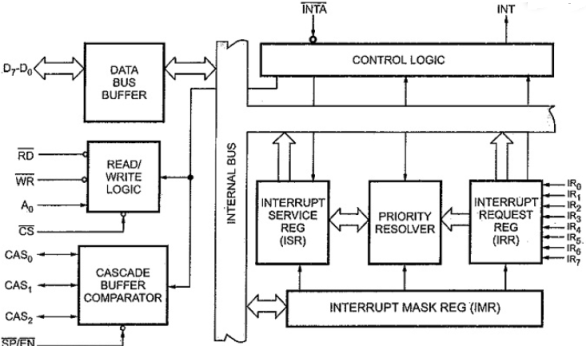
Fig 2 Block Diagram of 8259Data Bus Buffer:The data bus buffer allows the 8086 to send control words to the 8259A. The 8-bit data bus buffer also allows the 8259A to send interrupt opcode and address of the interrupt service subroutine to the 8086.Read/Write Logic:The RD and WR inputs control the data flow on the data bus when the device is selected by asserting its chip select (CS) input low.Control Logic:This block has an input and an output line. If the 8259A is properly enabled, the interrupt request will cause the 8259A to assert its INT output pin high. Interrupt Request Register (IRR):It is used to store all the interrupt levels which are requesting the service. The eight interrupt inputs set corresponding bits of the Interrupt Request Register upon service request.Interrupt Service Register (ISR):It stores all the levels that are currently being serviced.Interrupt Mask Register (IMR):It stores the masking bits of the interrupt lines to be masked. This register can be programmed by an Operation Command Word (OCW). Priority Resolver:It determines the priorities of the bits set in the IRR. The bit corresponding to the highest priority interrupt input is set in the ISR during the INTA input.Cascade Buffer Comparator:It generates control signals necessary for cascade operations. It also generates Buffer-Enable signals. Here, the former is called a master, and the latter are called slaves. The 8259 can be set up as a master or a slave by the SP/EN pin.CAS0— CAS2For a master 8259, the CAS0-CAS2 pins are output pins, and for slave 8259, these are input pins. When the 8259 is a master (that is, when it accepts interrupt requests from other 8259s), the CALL opcode is generated by the Master in response to the first INTA.SP / EN (Slave Program /Enable Buffer):The SP/EN signal is tied high for the master. However it is grounded for the slave.
|
|
|
|
D3 | D2 | D1 | Bit/pin of port C selected |
0 | 0 | 0 | PC0 |
0 | 0 | 1 | PC1 |
0 | 1 | 0 | PC2 |
0 | 1 | 1 | PC3 |
1 | 0 | 0 | PC4 |
1 | 0 | 1 | PC5 |
1 | 1 | 0 | PC6 |
1 | 1 | 1 | PC7 |
A1 | A0 | RD | WR | CS | Result |
0 | 0 | 1 | 0 | 0 | Write Counter 0 |
0 | 1 | 1 | 0 | 0 | Write Counter 1 |
1 | 0 | 1 | 0 | 0 | Write Counter 2 |
1 | 1 | 1 | 0 | 0 | Write Control Word |
0 | 0 | 0 | 1 | 0 | Read Counter 0 |
0 | 1 | 0 | 1 | 0 | Read Counter 1 |
1 | 0 | 0 | 1 | 0 | Read Counter 2 |
1 | 1 | 0 | 1 | 0 | No operation |
X | X | 1 | 1 | 0 | No operation |
X | X | X | X | 1 | No operation |
|
It is a control block for overall device. It controls the overall working by selecting the operation to be done. The operation selection depends upon input signals as:
|
|
|
0 matching results found
