Unit 4
Data Acquisition Methods
Q1. Explain the block diagram of the data acquisition model?
Sol:
A generalized data acquisition system block diagram is shown in Figure.
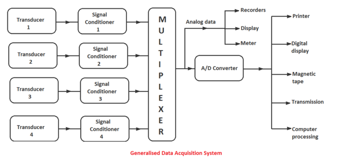
Figure 1. Data Acquisition System
The function of each block is as under:
Transducers: They are converting physical quantities (such as temperature, pressure, etc.) into electrical quantities, or measuring electrical quantities directly. They collect data from the physical world.
The most used transducers are:
RTD, Thermistor for temperature measurements.
Photosensors for light measurements.
Strain gauges, piezoelectric transducers for force and pressure measurements.
Microphone for sound measurements.
Potentiometer, LVDT, optical encoder for the position, and displacement measurements.
Signal Conditioning Unit: The signal produced by the transducers may or may not be suitable for our system to work properly. It may be very weak, strong, or may have some noise.
To convert this signal into the most suitable form, amplification, and filtration is done respectively by signal conditioning unit. So, the signal conditioning unit converts electrical signals into the most suitable form.
Multiplexer: The multiplexer receives multiple analog inputs and provides a single output signal according to the requirements.
If a separate channel is used for each quantity, the cost of installation, maintenance, and periodic replacement becomes high. Therefore, a single channel is used which is shared by various quantities.
Analog to Digital (A/D) Converters: The data is converted into digital form by A/D converters. After the conversion of data into digital form, it is displayed with the help of oscilloscopes, numerical displays, panel meters to monitor the complete system.
The data can be either permanently or temporarily stored or recorded according to the requirement. The data is recorded on optical, ultraviolet, stylus, or ink recorders for future use.
Q2. Explain Analog and Digital IO ?
Sol:
At the simplest level, data acquisition hardware is characterized by the subsystems it possesses. A subsystem is a component of your data acquisition hardware that performs a specialized task.
Common subsystems include
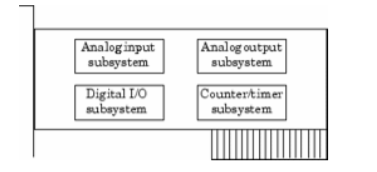
Figure. Analog and Digital IO
Analog input subsystems are also referred to as AI subsystems, A/D converters, or ADCs. Analog Output Subsystems Analog output subsystems convert digital data stored on your computer to a real-world analog signal. These subsystems perform the inverse conversion of analog input subsystems.
Typical acquisition boards offer two output channels with 12 bits of resolution, with special hardware available to support multiple channel analog output operations.
Digital Input/output Subsystems Digital input/output (DIO) subsystems are designed to input and output digital values (logic levels) to and from hardware. These values are typically handled either as single bits or lines or as a port, which typically consists of eight lines.
Q3. Explain successive approximation ADC?
Sol:
Successive Approximation
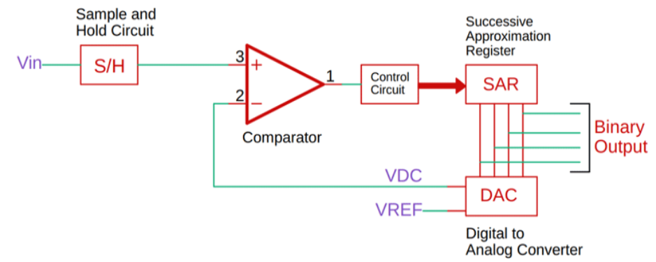
Figure. Successive approximation ADC
ADC consists of a comparator, a digital to analog converter, and a successive approximation register along with the control circuit.
Whenever a new conversation starts, the sample and hold samples the input signal. And that signal is compared with the specific output signal of the DAC.
Consider the sampled input signal is 5.8V. The reference of the ADC is 10V. When the conversion starts, the successive approximation register sets the most significant bit to 1 and all other bits to zero. This means the value becomes 1, 0, 0, 0, which means, for a 10V reference voltage, the DAC will produce a value of 5V which is half of the reference voltage.
Now this voltage will be compared to the input voltage and based on the comparator output, the output of the successive approximation register will be changed.
This means if Vin is greater than the output of the DAC, the most significant bit will stay as it is, and the next bit will be set for a new comparison. Otherwise, if the input voltage is less than the DAC value, the most significant bit will be set to zero, and the next bit will be set to 1 for a new comparison. This process will continue until the value closest to the input voltage reaches.
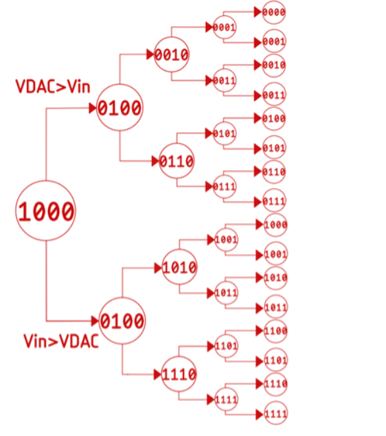
Figure. Conversion Time
Q4. Explain sigma-delta ADC?
Sol:

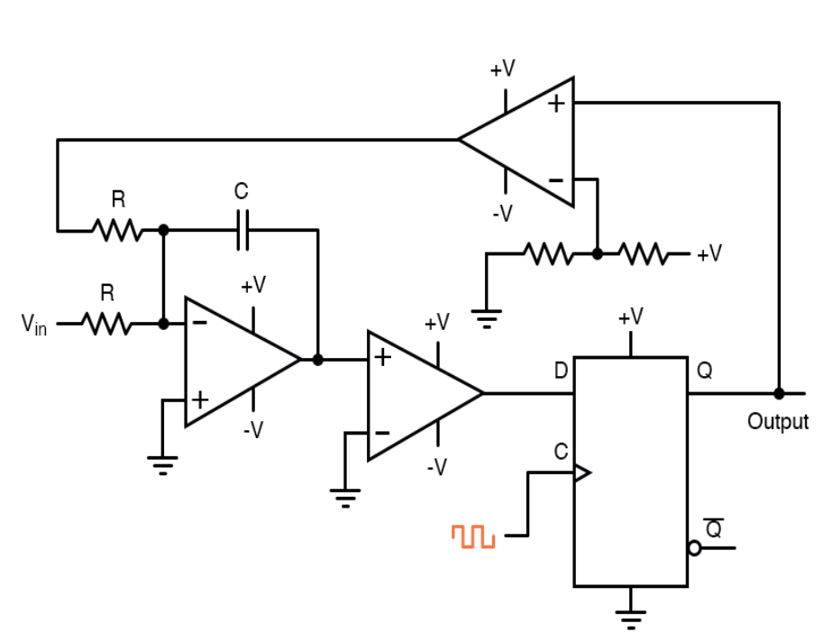
The leftmost op-amp is the (summing) integrator. The next op-amp the integrator feeds into is the comparator or 1-bit ADC. Next comes the D-type flip-flop, which latches the comparator’s output at every clock pulse, sending either a “high” or “low” signal to the next comparator at the top of the circuit.
This final comparator is necessary to convert the single-polarity 0V / 5V logic level output voltage of the flip-flop into a +V / -V voltage signal to be fed back to the integrator. If the integrator output is positive, the first comparator will output a “high” signal to the D input of the flip-flop.
At the next clock pulse, this “high” signal will be output from the Q line into the noninverting input of the last comparator. This last comparator, seeing an input voltage greater than the threshold voltage of 1/2 +V, saturates in a positive direction, sending a full +V signal to the other input of the integrator.
This +V feedback signal tends to drive the integrator output in a negative direction. If that output voltage ever becomes negative, the feedback loop will send a corrective signal (-V) back around to the top input of the integrator to drive it in a positive direction.
This is the delta-sigma concept in action: the first comparator senses a difference (Δ) between the integrator output and zero volts. The integrator sums (Σ) the comparator’s output with the analog input signal.
Output :
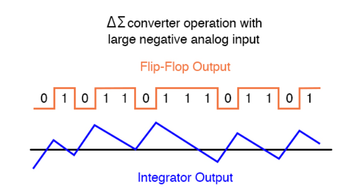
Figure. For large negative analog input
If we apply a negative analog input voltage, the integrator will tend to ramp its output in a positive direction.
Feedback can only add to the integrator’s ramping by a fixed voltage over a fixed time, and so the bitstream output by the flip-flop will not be quite the same:
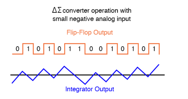
Figure. For small negative input
By applying a more negative analog input signal to the integrator, we force its output to ramp more steeply in a positive direction. Thus, the feedback system has to output more 1’s than before to bring the integrator output back to zero volts:
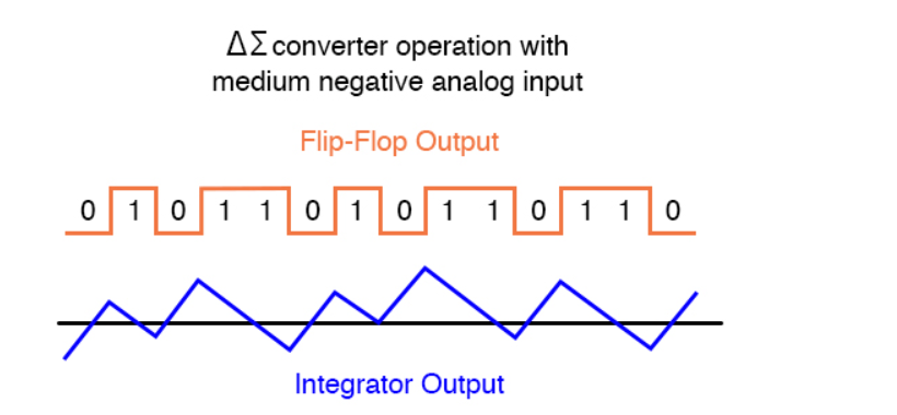
Figure. For medium negative input
As the analog input signal increases in magnitude, so does the occurrence of 1’s in the digital output of the flip-flop:

Figure. For high negative input
A parallel binary number output is obtained from this circuit by averaging the serial stream of bits together.
Q5. Explain binary-weighted DAC?
Sol:
Weighted Resistor DAC
A weighted resistor DAC produces an analog output, which is equal to the digital (binary) input by using binary-weighted resistors in the inverting adder circuit. In short, a binary-weighted resistor DAC is called a weighted resistor DAC.
The circuit diagram of a 3-bit binary-weighted resistor DAC is shown in the following figure −

Figure. Binary weighted DAC
The bits of a binary number can have only one of the two values. i.e., either 0 or 1. Let the 3-bit binary input is b2b1b0. Here, the bits b2 and b0 denote the Most Significant Bit (MSB) and Least Significant Bit (LSB) respectively.
The digital switches shown in the above figure will be connected to the ground when the corresponding input bits are equal to ‘0’
Similarly, the digital switches shown in the above figure will be connected to the negative reference voltage, −VR when the corresponding input bits are equal to ‘1’.
In the above circuit, the non-inverting input terminal of an op-amp is connected to the ground. That means zero volts is applied at the non-inverting input terminal of op-amp.
According to the virtual short concept, the voltage at the inverting input terminal of the opamp is the same as that of the voltage present at its non-inverting input terminal. So, the voltage at the inverting input terminal’s node will be zero volts.
The nodal equation at the inverting input terminal’s node is:
(0 + VR b2) / 2 0 R + 0 + VR b1 / 2 1 R + 0 + VR b0 / 2 2 R + 0 -V0 /Rf =0
Vo /Rf = VR b2 / 2 0 R + VR b1 / 2 1 R + VR b0 / 2 2 R
Vo = VR .Rf/ R { b2 / 2 0 + b1 / 2 1 + b0 / 2 2 }
Substituting R = 2Rf in the above equation
Vo = VR . Rf / 2 Rf { b2 / 2 0 + b1 / 2 1 + b0 / 2 2 }
Vo = VR / 2 { b2 / 2 0 + b1 / 2 1 + b0 / 2 2 }
The above equation represents the output voltage equation of a 3-bit binary weighted resistor DAC. Since the number of bits are three in the binary (digital) input, we will get seven possible values of output voltage by varying the binary input from 000 to 111 for a fixed reference voltage, VR.
We can write the generalized output voltage equation of an N-bit binary weighted resistor DAC as shown below based on the output voltage equation of a 3-bit binary-weighted resistor DAC.
=>V0=VR/2{bN−1/20+bN−2/21+....+b0/2N−1}
Q6. Explain R-2R Ladder DAC?
Sol:
The R-2R Ladder DAC overcomes the disadvantages of a binary-weighted resistor DAC. As the name suggests, R-2R Ladder DAC produces an analog output, which is almost equal to the digital (binary) input by using an R-2R ladder network in the inverting adder circuit.
The circuit diagram of a 3-bit R-2R Ladder DAC is shown in the following figure

Figure. R-2R ladder DAC
Let the 3-bit binary input is b2b1b0. Here, the bits b2 and b0 denote the Most Significant Bit (MSB) and Least Significant Bit (LSB) respectively.
The digital switches shown in the above figure will be connected to the ground when the corresponding input bits are equal to ‘0’. Similarly, the digital switches shown in the above figure will be connected to the negative reference voltage, −VR when the corresponding input bits are equal to ‘1’.
It is difficult to get the generalized output voltage equation of an R-2R Ladder DAC. But, we can find the analog output voltage values of R-2R Ladder DAC for individual binary input combinations easily.
Q7. What are the advantages of r-2r?
Sol:
Q8. What are the disadvantages of Binary Weighted?
Sol:
The disadvantages of a binary-weighted resistor DAC are as follows −
Q9. What is a socket?
Sol:
A network socket is a software structure within a network node of a computer network that serves as an endpoint for sending and receiving data across the network. The structure and properties of a socket are defined by an application programming interface (API) for the networking architecture.
Q10. Explain the use of Data Sockets for Networked Communication
Sol:
A socket is created by concatenating the IP number of a system and a software port number. This allows the process to know the address of the system the IP address and the address where the information needs to be sent the port number. The IP number and the port number are separated by a :

Figure Data Sockets
The diagram above shows two different applications communicating with one another through sockets.
In this diagram, application 1 sends the data to IP number 192.168.16.21 of application 2, port 100 while application 2 sends the data to IP number 192.168.1.1 of application 1, port 80.
Unit 4
Data Acquisition Methods
Q1. Explain the block diagram of the data acquisition model?
Sol:
A generalized data acquisition system block diagram is shown in Figure.

Figure 1. Data Acquisition System
The function of each block is as under:
Transducers: They are converting physical quantities (such as temperature, pressure, etc.) into electrical quantities, or measuring electrical quantities directly. They collect data from the physical world.
The most used transducers are:
RTD, Thermistor for temperature measurements.
Photosensors for light measurements.
Strain gauges, piezoelectric transducers for force and pressure measurements.
Microphone for sound measurements.
Potentiometer, LVDT, optical encoder for the position, and displacement measurements.
Signal Conditioning Unit: The signal produced by the transducers may or may not be suitable for our system to work properly. It may be very weak, strong, or may have some noise.
To convert this signal into the most suitable form, amplification, and filtration is done respectively by signal conditioning unit. So, the signal conditioning unit converts electrical signals into the most suitable form.
Multiplexer: The multiplexer receives multiple analog inputs and provides a single output signal according to the requirements.
If a separate channel is used for each quantity, the cost of installation, maintenance, and periodic replacement becomes high. Therefore, a single channel is used which is shared by various quantities.
Analog to Digital (A/D) Converters: The data is converted into digital form by A/D converters. After the conversion of data into digital form, it is displayed with the help of oscilloscopes, numerical displays, panel meters to monitor the complete system.
The data can be either permanently or temporarily stored or recorded according to the requirement. The data is recorded on optical, ultraviolet, stylus, or ink recorders for future use.
Q2. Explain Analog and Digital IO ?
Sol:
At the simplest level, data acquisition hardware is characterized by the subsystems it possesses. A subsystem is a component of your data acquisition hardware that performs a specialized task.
Common subsystems include

Figure. Analog and Digital IO
Analog input subsystems are also referred to as AI subsystems, A/D converters, or ADCs. Analog Output Subsystems Analog output subsystems convert digital data stored on your computer to a real-world analog signal. These subsystems perform the inverse conversion of analog input subsystems.
Typical acquisition boards offer two output channels with 12 bits of resolution, with special hardware available to support multiple channel analog output operations.
Digital Input/output Subsystems Digital input/output (DIO) subsystems are designed to input and output digital values (logic levels) to and from hardware. These values are typically handled either as single bits or lines or as a port, which typically consists of eight lines.
Q3. Explain successive approximation ADC?
Sol:
Successive Approximation

Figure. Successive approximation ADC
ADC consists of a comparator, a digital to analog converter, and a successive approximation register along with the control circuit.
Whenever a new conversation starts, the sample and hold samples the input signal. And that signal is compared with the specific output signal of the DAC.
Consider the sampled input signal is 5.8V. The reference of the ADC is 10V. When the conversion starts, the successive approximation register sets the most significant bit to 1 and all other bits to zero. This means the value becomes 1, 0, 0, 0, which means, for a 10V reference voltage, the DAC will produce a value of 5V which is half of the reference voltage.
Now this voltage will be compared to the input voltage and based on the comparator output, the output of the successive approximation register will be changed.
This means if Vin is greater than the output of the DAC, the most significant bit will stay as it is, and the next bit will be set for a new comparison. Otherwise, if the input voltage is less than the DAC value, the most significant bit will be set to zero, and the next bit will be set to 1 for a new comparison. This process will continue until the value closest to the input voltage reaches.

Figure. Conversion Time
Q4. Explain sigma-delta ADC?
Sol:
The leftmost op-amp is the (summing) integrator. The next op-amp the integrator feeds into is the comparator or 1-bit ADC. Next comes the D-type flip-flop, which latches the comparator’s output at every clock pulse, sending either a “high” or “low” signal to the next comparator at the top of the circuit.
This final comparator is necessary to convert the single-polarity 0V / 5V logic level output voltage of the flip-flop into a +V / -V voltage signal to be fed back to the integrator. If the integrator output is positive, the first comparator will output a “high” signal to the D input of the flip-flop.
At the next clock pulse, this “high” signal will be output from the Q line into the noninverting input of the last comparator. This last comparator, seeing an input voltage greater than the threshold voltage of 1/2 +V, saturates in a positive direction, sending a full +V signal to the other input of the integrator.
This +V feedback signal tends to drive the integrator output in a negative direction. If that output voltage ever becomes negative, the feedback loop will send a corrective signal (-V) back around to the top input of the integrator to drive it in a positive direction.
This is the delta-sigma concept in action: the first comparator senses a difference (Δ) between the integrator output and zero volts. The integrator sums (Σ) the comparator’s output with the analog input signal.
Output :

Figure. For large negative analog input
If we apply a negative analog input voltage, the integrator will tend to ramp its output in a positive direction.
Feedback can only add to the integrator’s ramping by a fixed voltage over a fixed time, and so the bitstream output by the flip-flop will not be quite the same:

Figure. For small negative input
By applying a more negative analog input signal to the integrator, we force its output to ramp more steeply in a positive direction. Thus, the feedback system has to output more 1’s than before to bring the integrator output back to zero volts:

Figure. For medium negative input
As the analog input signal increases in magnitude, so does the occurrence of 1’s in the digital output of the flip-flop:
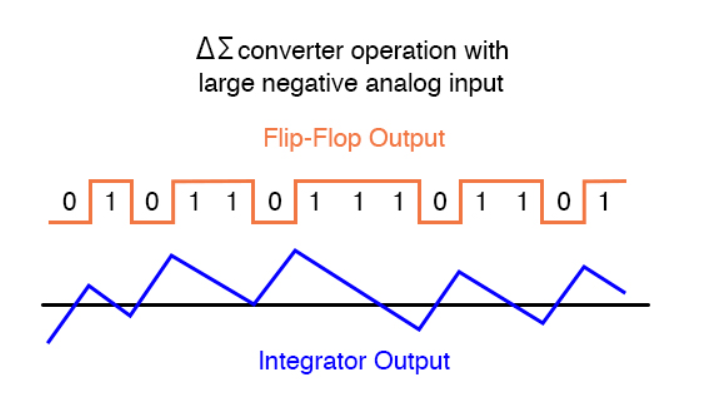
Figure. For high negative input
A parallel binary number output is obtained from this circuit by averaging the serial stream of bits together.
Q5. Explain binary-weighted DAC?
Sol:
Weighted Resistor DAC
A weighted resistor DAC produces an analog output, which is equal to the digital (binary) input by using binary-weighted resistors in the inverting adder circuit. In short, a binary-weighted resistor DAC is called a weighted resistor DAC.
The circuit diagram of a 3-bit binary-weighted resistor DAC is shown in the following figure −
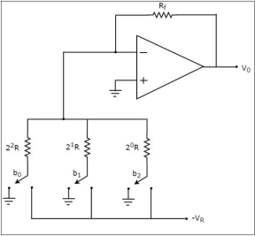
Figure. Binary weighted DAC
The bits of a binary number can have only one of the two values. i.e., either 0 or 1. Let the 3-bit binary input is b2b1b0. Here, the bits b2 and b0 denote the Most Significant Bit (MSB) and Least Significant Bit (LSB) respectively.
The digital switches shown in the above figure will be connected to the ground when the corresponding input bits are equal to ‘0’
Similarly, the digital switches shown in the above figure will be connected to the negative reference voltage, −VR when the corresponding input bits are equal to ‘1’.
In the above circuit, the non-inverting input terminal of an op-amp is connected to the ground. That means zero volts is applied at the non-inverting input terminal of op-amp.
According to the virtual short concept, the voltage at the inverting input terminal of the opamp is the same as that of the voltage present at its non-inverting input terminal. So, the voltage at the inverting input terminal’s node will be zero volts.
The nodal equation at the inverting input terminal’s node is:
(0 + VR b2) / 2 0 R + 0 + VR b1 / 2 1 R + 0 + VR b0 / 2 2 R + 0 -V0 /Rf =0
Vo /Rf = VR b2 / 2 0 R + VR b1 / 2 1 R + VR b0 / 2 2 R
Vo = VR .Rf/ R { b2 / 2 0 + b1 / 2 1 + b0 / 2 2 }
Substituting R = 2Rf in the above equation
Vo = VR . Rf / 2 Rf { b2 / 2 0 + b1 / 2 1 + b0 / 2 2 }
Vo = VR / 2 { b2 / 2 0 + b1 / 2 1 + b0 / 2 2 }
The above equation represents the output voltage equation of a 3-bit binary weighted resistor DAC. Since the number of bits are three in the binary (digital) input, we will get seven possible values of output voltage by varying the binary input from 000 to 111 for a fixed reference voltage, VR.
We can write the generalized output voltage equation of an N-bit binary weighted resistor DAC as shown below based on the output voltage equation of a 3-bit binary-weighted resistor DAC.
=>V0=VR/2{bN−1/20+bN−2/21+....+b0/2N−1}
Q6. Explain R-2R Ladder DAC?
Sol:
The R-2R Ladder DAC overcomes the disadvantages of a binary-weighted resistor DAC. As the name suggests, R-2R Ladder DAC produces an analog output, which is almost equal to the digital (binary) input by using an R-2R ladder network in the inverting adder circuit.
The circuit diagram of a 3-bit R-2R Ladder DAC is shown in the following figure
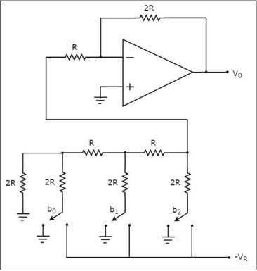
Figure. R-2R ladder DAC
Let the 3-bit binary input is b2b1b0. Here, the bits b2 and b0 denote the Most Significant Bit (MSB) and Least Significant Bit (LSB) respectively.
The digital switches shown in the above figure will be connected to the ground when the corresponding input bits are equal to ‘0’. Similarly, the digital switches shown in the above figure will be connected to the negative reference voltage, −VR when the corresponding input bits are equal to ‘1’.
It is difficult to get the generalized output voltage equation of an R-2R Ladder DAC. But, we can find the analog output voltage values of R-2R Ladder DAC for individual binary input combinations easily.
Q7. What are the advantages of r-2r?
Sol:
Q8. What are the disadvantages of Binary Weighted?
Sol:
The disadvantages of a binary-weighted resistor DAC are as follows −
Q9. What is a socket?
Sol:
A network socket is a software structure within a network node of a computer network that serves as an endpoint for sending and receiving data across the network. The structure and properties of a socket are defined by an application programming interface (API) for the networking architecture.
Q10. Explain the use of Data Sockets for Networked Communication
Sol:
A socket is created by concatenating the IP number of a system and a software port number. This allows the process to know the address of the system the IP address and the address where the information needs to be sent the port number. The IP number and the port number are separated by a :
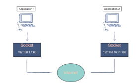
Figure Data Sockets
The diagram above shows two different applications communicating with one another through sockets.
In this diagram, application 1 sends the data to IP number 192.168.16.21 of application 2, port 100 while application 2 sends the data to IP number 192.168.1.1 of application 1, port 80.