Unit – 3
Generation and recombination of carriers
Q1) The voltage gain of an amplifier without feedback is 3000. Calculate the voltage gain of the amplifier if negative voltage feedback is introduced in the circuit. Given that feedback fraction mv = 0.01.
A1)

Voltage gain with negative feedback is

Q2) The overall gain of a multistage amplifier is 140. When negative voltage feedback is applied, the gain is reduced to 17.5. Find the fraction of the output that is feedback to the input.
A2)

Let  be the feedback fraction. Voltage gain with negative feedback is


Q3) When negative voltage feedback is applied to an amplifier of gain 100, the
overall gain falls to 50.
(i) Calculate the fraction of the output voltage feedback.
(ii) If this fraction is maintained, calculate the value of the amplifier gain required if the overall stage gain is to be 75.
A3)
(i) Gain without feedback, 
Gain with feedback, 
Let  be the fraction of the output voltage feedback.

(ii) 


Q4) With a negative voltage feedback, an amplifier gives an output of 10 V with an input of 0.5 V. When feedback is removed, it requires 0.25 V input for the same output. Calculate (i) gain without feedback (ii) feedback fraction mv.
A4)
(i) Gain without feedback, 
(ii) Gain with feedback, 
Now 


Q5) The gain of an amplifier without feedback is 50 whereas with negative voltage feedback, it falls to 25. If due to ageing, the amplifier gain falls to 40, find the percentage reduction in stage gain (i) without feedback and (ii) with negative feedback.
A5)


(i) Without feedback.
The gain of the amplifier without feedback is 50. However, due to ageing it falls to 40.
 %age reduction in stage gain
(ii) With negative feedback
When the gain without feedback was 50, the gain with negative feedback was 25. Now the gain without feedback falls to 40.
 New gain with negative feedback
 % age reduction in stage gain
Q6) An amplifier has a voltage amplification Av and a fraction mv of its output is feedback in opposition to the input. If mv = 0.1 and Aν = 100, Calculate the percentage change in the gain of the system if Aν falls 6 db due to ageing.
A6)


Fall in gain=6db
Let  be the new absolute voltage gain without feedback.


 age change in system gain
Q7) An amplifier has a voltage gain of 500 without feedback. If a negative feedback is applied, the gain is reduced to 100. Calculate the fraction of the output fed back. If, due to ageing of components, the gain without feedback falls by 20%, calculate the percentage fall in gain with feedback.
A7)


Q8) An amplifier has an open-loop gain Av = 100,000. A negative feedback of 10 db is applied. Find (i) voltage gain with feedback (ii) value of feedback fraction mv.
A8)
 voltage gain without feedback

Voltage gain with feedback=100-10=90db
Now 


(ii) 


Q9) An amplifier with an open-circuit voltage gain of 1000 has an output resistance of 100 Ω and feeds a resistive load of 900 Ω. Negative voltage feedback is provided by connecting a resistive voltage divider across the output and one-fiftieth of the output voltage is feedback in series with the input signal. Determine the voltage gain with negative feedback.

A9)
Voltage gain of the amplifier without feedback is:


Q10) An amplifier is required with a voltage gain of 100 which does not vary by more than 1%. If it is to use negative feedback with a basic amplifier the voltage gain of which can vary by 20%, determine the minimum voltage gain required and the feedback factor.
A10)

Also 

Multiplying eq(i) by  we have

Substracting [(ii)-(iii)], we have
19.8=0.008
Putting the value of 


Q11) An amplifier has a gain of 1000 without feedback and cut-off frequencies are f1 = 1.5 kHz and f2 = 501.5 kHz. If 1% of output voltage of the amplifier is applied as negative feedback, what are the new cut-off frequencies?
A11)

The new lower cut-off frequency with feedback is

The new upper cut-off frequency with feedback is

Q12) The current gain of an amplifier is 200 without feedback. When negative
current feedback is applied, determine the effective current gain of the amplifier. Given that current attenuation mi = 0.012.
A12)

Here 

Q13) For the emitter follower circuit shown in Figure, find the input impedance.
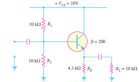
A13)
Voltage across 
Voltage across 
Emitter current, 
 A.C. Emitter resistance,
Effective external emitter resistance is


 Input impedance of the emitter follower is


Q14) For the emitter follower circuit shown in Figure, find the input impedance.
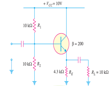
A14)
Voltage across 
Voltage across 
 Emitter current,
 A.C emitter resisitance
Effective external emitter resistance is


 Input impedance of the emitter follower is


Q15) For the Darlington amplifier in Figure, find (i) the d.c. Levels of both the
transistors and (ii) a.c. Emitter resistances of both transistors.
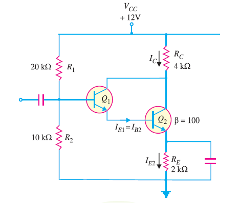
A15)
(i) D.C Bias Levels
Base voltage of 
Emitter voltage of 
Emitter voltage of 

(ii) A.C Analysis
A.C emitter resistance of 
A.C emitter resistance of 
Q16) Calculate the value of resistor RC so that the voltage gain of the amplifier in fig is 100. Capacitors C1, C2, and C3 may be assumed short at signal frequency.
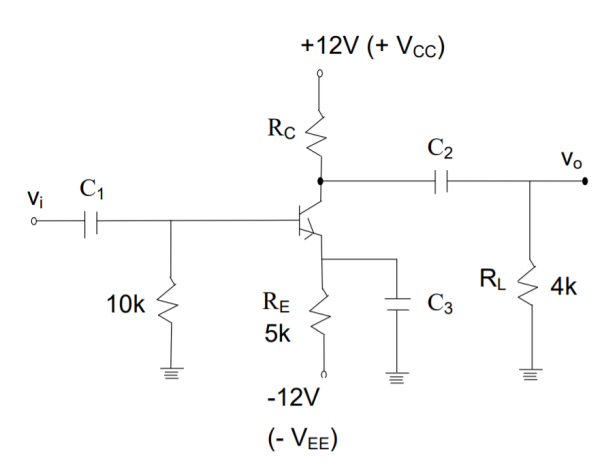
A16)
In case, RE is by-passed, the voltage gain Av of the amplifier is,

Where rc is the effective (ac) resistance seen by the collector of the transistor, and ' e r is the dynamic resistance of the emitter. We know,


Where resistances have been taken in kΩ. Therefore,

As  (given),
  is,
is,


Q17) Find out the smallest value of load RL in the amplifier circuit shown in fig so that the voltage gain is at least 40. The dynamic emitter resistance of the transistor is 25 Ω. The coupling and by-pass capacitors may be assumed short at signal frequency.
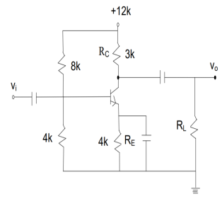
A17)
The voltage gain of the common emitter amplifier with resistor RE by-passed (see fig.) is expressed as
Ssed as

Where rc is effective ac impedance seen by the collector Which, is


Q18) The silicon transistor in the common- base amplifier has the current gain α of 0.98. Find the input impedance and voltage gain of the amplifier in fig. (VBE = 0.7V)
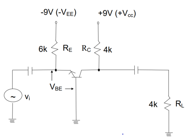
A18)
The dc voltage sources have to be grounded for ac analysis of the amplifier. Then the input impedance of the CB amplifier (in fig.) is

Where r’e is dynamic emitter resiatance and r’e << RE

Where IE is dc emitter current in the circuit

 Thus, the input impedance Zi(amp) is,

The low value of input impedance is the main reason for limited applications of CB amplifier. The voltage gain of CB amplifier is expressed as,
Since, 
Then, 
Q19) The transistor in the amplifier circuit shown in fig, has h – parameters, hie = 2kΩ and hfl = 80. The values of hoe and hre are negligible. Calculate the voltage gain and input impedance Zi(amp) of the amplifier. Capacitors C1, C2, and C3 may be assumed short at signal frequency due to small impedances.

A19)
The magnitude of voltage gain with h-parameters hoe and hre dropped, and emitter resistance RE by-passed by capacitor C3 is

Because the ac load at collector, Zl, is

Further, the impedance between base and ground, Zi(base) is,

And, input impedance of amplifier, Zi(amp) is


Q20) The emitter follower (common collector amplifier) shown in fig. Uses a transistor with h-parameters hie = 4.5 kΩ, hfe = 120. Other parameters hoe and hre have negligible effect on amplifier performance. Calculate voltage gain and input impedance of the amplifier. The coupling and by-pass capacitors may be assumed short at signal frequency.
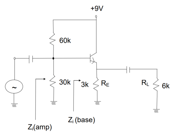
A20)
Neglecting the effect of hoe and hre on amplifier performance, the voltage gain of emitter follower may be expressed as,

Where Ze is the effective load seen by the emitter, and it is

And using hfc ≈ hfe and hic = hie,


The input impedance as seen at the base w.r.t ground is,

The input impedance of the amplifier (that is, after taking the effect of biasing resistors)

And the effective base resistance RB is,


