Unit – 5
MOS capacitor
Q1) The MOSFET circuit shown below uses a MOSFET with the indicated characteristics. For each of the cases listed, solve MOSFET’s device current and drain voltage, and indicate whether the device is operating in saturation or triode. Given Kn = 250µA/ V2 VThN = 0.5V
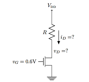
(A) R = 100Ω (B) R = 1kΩ (C) R = 10kΩ?
A1) If the device is in saturation, then the device’s current and drain voltage are:

Where vOV = vG − VTh = 0.1 V. If the device is in triode, then the solution is more complex:


Since the triode solution is more complex, it’s easier to first assume saturation and see if the result is consistent with that assumption. In saturation, the device current should always be 2.5 µA.
(A) R = 100Ω — In this case, we find

This result is consistent with being in saturation since vD > vOV.
(B) R = 1kΩ — In this case, we find

This result is consistent with being in saturation since vD > vOV.
(C) R = 10kΩ— In this case, we find

This result is consistent with being in saturation since vD > vOV.
Q2) The MOSFET circuit shown below uses a MOSFET with the indicated characteristics. For each of the cases listed, solve MOSFET’s device current and drain voltage, and indicate whether the device is operating in saturation or triode. Kn = 250µA/ V2 VThN = 0.5V
(A) R = 100Ω (B) R = 1kΩ (C) R = 10kΩ
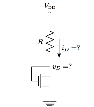
A2) In this problem, the device is always in saturation due the diode connection, which guarantees vDS > vOV in all cases. The solution requires solving a quadratic


It is perhaps quickest to solve for vOV:


Now we can use the quadratic formula to solve


In the numerator, we choose ‘+’ from the ‘±’ in order to obtain a positive-valued solution (a negative valued solution doesn’t make physical sense).
(A) R = 100Ω — In this case, we find


(B) R = 1kΩ — In this case, we find


(C) R = 10kΩ — In this case, we find


Q3) The MOSFET circuit shown below uses a MOSFET with the indicated characteristics. For each of the cases listed, solve MOSFET’s device current and drain voltage, and indicate whether the device is operating in saturation or triode. Kn = 250µA/ V2 VThN = 0.5V. (A) R = 100Ω (B) R = 1kΩ (C) R = 10kΩ
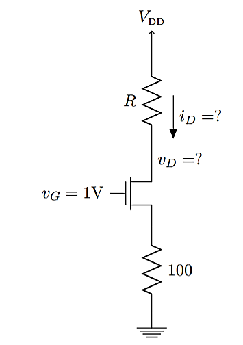
A3) In this problem, we can use the same procedure from Problem 1. Since RS is small, it should have a minor effect on the DC solution. We can evaluate that effect by iterating as follows:


If we initially assume vS = 0, then we can solve for a new vS, then repeat the equations until the results stabilizes. From this procedure, we find the following

As long as the device stays in saturation, these results should not depend on R and will be the same for each case. Then the solutions are:
(A) R = 100Ω


(B) R = 1kΩ:


(C) R = 10kΩ


Q4) The MOSFET circuit shown below uses a pair of identical MOSFETs with the indicated characteristics. For each of the cases listed, solve MOSFETs’ device currents and drain voltages, and indicate whether each device is operating in saturation or triode. Kn = 250µA/ V2, VThN = 0.5V. (A) R = 100Ω (B) R = 1kΩ (C) R = 10kΩ.
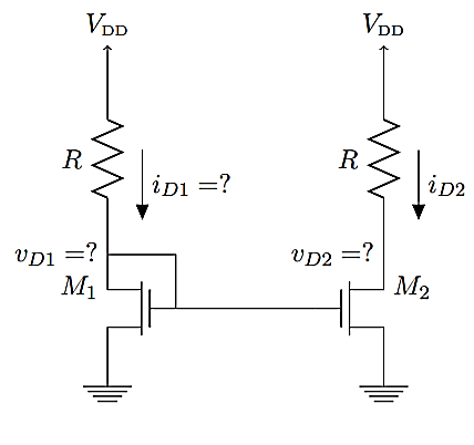
A4) Notice that the left-hand side of this circuit is identical to the one in Problem 2. The solution should be exactly the same. On the right hand side, there is an identical MOSFET and an identical resistor. Furthermore, the two MOSFETs share identical gate and source voltages, and should therefore have identical currents (iD2 = iD1 in all cases). With all other things being equal, the only remaining unknown (vD2) should also be identical to its twin on the right-hand side. This is called a symmetry argument, and is a very useful method for analyzing current mirrors and differential circuits.
Q5) The MOSFET circuit shown below uses a MOSFET with the indicated characteristics. For each of the cases listed, solve MOSFET’s device current and drain voltage, and indicate whether the device is operating in saturation or triode. Kp = 75µA/ V2, VThP = 0.75V. (A) R = 100Ω (B) R = 1kΩ (C) R = 10kΩ
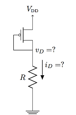
A5) This problem is nearly identical to Problem 2, except that the PMOS device has a different k value and the voltages are “upside down”. By modifying the solution for Problem 2, we obtain:


Notice that this is exactly the same equation as in Problem 2, except VTh and k
Are numerically different. So, we just need to repeat the quadratic equation from
Problem 2 to get the results:
(A) R = 100:

(B) R = 1k

(C) R = 10k:

Q6) The MOSFET circuit shown below uses a MOSFET with the indicated characteristics. For each of the cases listed, solve MOSFET's device current and drain voltage, and indicate whether the device is operating in saturation or triode. Kp = 75μA/ V2, VThP = 0:75V. (A) R = 100 (B) R = 1k (C) R = 10k?
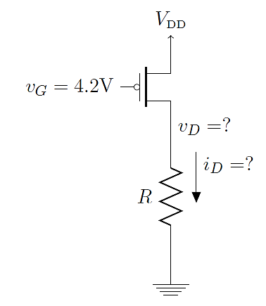
A6) This problem is very similar to Problem 1. We begin by assuming the device is in
Saturation, then solve for iD, then for vD, and finally verify that the device is in
Saturation.


Applying these solutions to each of the cases:
(A) R = 100:
vD = 9:37 μV
(B) R = 1k:
vD = 93:7 μV
(C) R = 10k:
vD = 937 μV
Q7) The MOSFET circuit shown below uses a MOSFET with the indicated characteristics. For each of the cases listed, solve MOSFET's device current and drain voltage, and indicate whether the device is operating in saturation or triode. Kp = 75μA/ V2, VThP = 0:75V, R = 1k. (A) vG = 4:5V (B) vG = 4:0V (C) vG = 3:0V (D) Assuming the device is in deep triode (i.e. it is in the linear region), solve for the case when vG = 0V by approximating the device as a resistor with resistance RON.
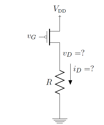
A7) Again, begin by assuming the device is in saturation. Then we have


Saturation 
Applying this to the four cases
(A) vG = 4.5V


(B) vG = 4.0V


(C) vG = 3.0V


(D) vG = 0V: Here the device is obviously in triode. As an initial guess, we can assume |vDS| = 0, so that vD = VDD, but then some current must be flowing through R, so |vDS| must be greater than zero. To estimate the value of |vDS|, we can use a Taylor approximation

By solving the derivative in the above equation, we find that the “on resistance” is given by

Then we can use a voltage-divider to predict vD

This result can be used as an initial guess for iterating with the triode formula. Upon iteration, we obtain a more precise answer of vD = 0.677 V. These results indicate that this device is not very good at pulling up the output voltage across a 1 kΩ load.
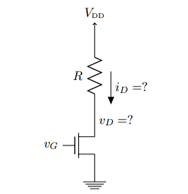
Q8) The MOSFET circuit shown below uses a MOSFET with the indicated characteristics. For each of the cases listed, solve MOSFET’s device current and drain voltage, and indicate whether the device is operating in saturation or triode. [Hint: To perform this analysis, the usual procedure is to assume the device is in saturation, and solve accordingly. Then check for consistency? Kn = 250µA/ V2 VThN = 0.5V R = 1kΩ. (A) vG = 0.25V (B) vG = 0.74V (C) vG = 3V (D) Assuming the device is in deep triode (i.e. it is in the linear region), solve for the case when vG = 5V by approximating the device as a resistor with resistance RON.
A8)
We begin by assuming saturation


Saturation 
Applying this to the four cases:
(A) vG = 0.25V


(B) vG = 0.74V


Saturation
(C) vG = 3.0V


(D) vG = VDD
Here the device is obviously in triode. As an initial guess, we can assume vD = 0 and use a Taylor approximation as before

Then we can use a voltage-divider to predict vD

This result can be used as an initial guess for iterating with the triode formula. Upon iteration, we obtain a more precise answer of vD = 2.82 V (so the RON voltage divider prediction was pretty close). These results indicate that this device is not very good at pulling down the output voltage across a 1 kΩ load
Q9) An amplifier has a signal i/p Vtg. Vi of 0.25v and draws 1mA from the source. The amɤ delivers & v to a load at 10 mA. Determine the current Vtg and power gains. Also find the i/p resistance of this ampɤ what must be the open ckt. Vtg of the source Vs to provide an ampɤ i/p VtgVi of 0.25 v when the internal resistance of the source is 50 Ω?
Given Vi = 0.25v, Ii = 1 Ma, Vo = 8 v, Io = 10 mA, Rs = 50 Ω.
A9)
Vtg gain Av =  =8/0.25 =32
Current gain 
Power gain AP = Av  = 32
= 32 
Input resistance Ri = = 250
= 250
Open circuit Vtg of Vs
Vi =
Vs = 
Vs = 
Vs = 0.3v
Q10) Calculate the value of feedback resistor Rs required to self bias JFET with IDSS= 40mA, VP= -10 and VGSQ= -5V?
A10)
IDQ =IDSS [1-(VGSQ/VP)]2
= 40x10-3 [1-{(-5)/(-10)}]2 = 10mA
For self-bias VGSQ = - IDQ RS
RS = -VGSQ/IDQ = -(-5)/10mA = 500Ohm
Q11) For the circuit shown below the FET has VP= 4V, IDSS = 4mA. Calculate IDSQ, VGSQ and VDSQ?
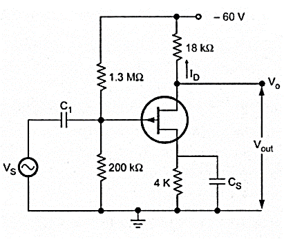
A11)
The simplified circuit will be
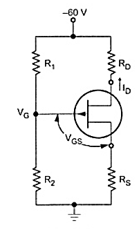
VG = R2 VDD/ (R1 + R2) = (200x10-3x(-60))/(1.3x106+200x103) = -8V
VG – VGS +ID RS = 0
VGS = -8 + ID RS
Finding ID
ID = IDSS (1-VGS/VP)2 = 2.25mA or 4mA
As the given circuit is of p-channel FET so VDS should be negative. For ID =2.25mA the value of VDS is negative.
VDS= VDD -ID (RD + RS) = -60-(-2.25m (4000+18000)) = -10.5V
VGS = -8 +ID R= = 1V
Q12) Compare the biasing of MOSFET and FET?
A12)
Type | Configuration | Pertinent equation | Graphical solution |
JFET 1  |
|     |
|
Depletion-type MOSFET Voltage-fixed bias |
|  
|
|
Depletion-type MOSFET Voltage-divider bias |
|    |
|
Enhancement type MOSFET Feedback configuration |
|   |
|
Enhancement type MOSFET Voltage-divider |
|  
|
|
Q13) For the circuit shown in figure calculate ID , VDS, VG and VS
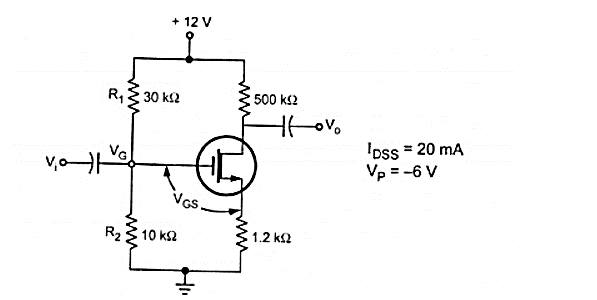
A13)
Applying KVL to the input circuit.
VGS = VG – VS
= 3 – IS RS Since VS = IS RS
= 3 – ID RS Since ID = IS
We have
ID = IDSS ( 1 – VGS / VP ) 2
Substituting the value of VGS we get
ID = IDSS ( 1 – (3 – ID RS)/Vp) 2 = 20 x 10 -3 ( 1 – ( 3 – ID x 1.2 x 10 3 / -6)
= 20 x 10 -3 ( 1 – [ (-0.5) + 200 ID ]) 2 = 20 x 10 -3 ( 1.5 -2)
= 20 x 10 -3 (2.25 – 600ID + 40000ID 2)
I D = 0.045 – 12 I D + 800 I D 2
800 I D 2 – 13 I D + 0.045 =0
Solving for quadratic equation we get
= -(-13) ± [ (13) 2 – 4(800)(0.045)] ½ / 2(800)
= 13 ± [ 169 -144] ½ / 1600 = 13 ±  / 1600 = 13 ± 5 /1600 = 5mA or 11.25 mA
If we calculate the value of VDS taking ID = 11.25mA we get
VDS = VDD – ID ( RD + RS)
= 12 – 11.25 x 10 -3 ( 500 + 1.2 x 10 3)
= 12 – 19.125 = -7.125
Practically the value of VDS must be positive hence ID= 11.25 mA is invalid
Hence take ID = 5mA
VDS = VDD – ID (RD + RS) = 12 – 5 x 10 -3 (500 + 1.2 x 10 3) = 12 – 8.5 = 3.5 V
VGS = 3 – ID RS = 3- 5 x 10 -3 x 1.2 x 10 3 = 3 – 6 = -3 V
Vs = ID RS = 5 x 10 -3 x 1.2 x 10 3 = 6V
Q14) For the circuit shown in figure assume that R1 = 30KΩ and R2 = 10 KΩ. Rd = 40KΩ. Vdd = 10V and VT=1V, Vgs = 2V and K = 0.1mA /V2. Find Id and VDS
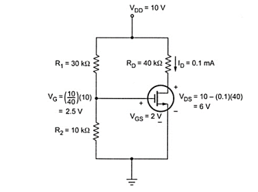
A14)
VG = VGS = (R2/R1+R2) VDD = (10/10+30) (10) = 2.5V
Assuming that the MOSFET is biased in the saturation region the drain current is
VDS = VDD – ID RD = 10 – (0.1)(40) = 6V.
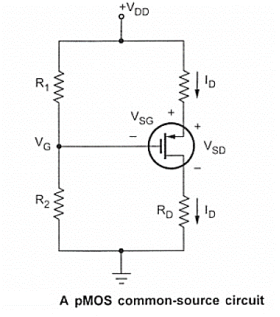
Here, the source is tied to +VDD, Which, become signal ground in the a.c. Equivalent circuit. Thus, it is also a common-source circuit.
The d.c. Analysis for this circuit is essentially the same as for the n-channel MOSFET circuit. The gate voltage is given by,
VG = (R2/R1 + R2) (VDD)
And the source to gate voltage is given by
VSG = VDD -VG
Assuming VGS <VT or VSG > |VT| the device in the saturation region and the drain current is given by
ID = K(VSG + VT) 2
And the source to drain voltage is given by
VSD = VDD – ID RD
If VSD > VSD (sat) then MOSFET is in saturation region.
IF VSD < VSD(sat) MOSFET is in non-saturation region.
Q15) Explain PIN diode?
A15) In p-i-n diode an “intrinsic” (actually lightly doped) I region is sandwiched between heavily doped p- and n-regions. It is p-i-n diode is a three-region structure
In the p-i-n photodiode shown schematically in Figure 21.An opening is made in the surface metallization to admit light, the top semiconductor region is kept very thin no minimize absorption in the region and the i-layer width is specifically tailored so achieve the desired response characteristics. Because of the low doping the i-layer is totally depleted under zero bias or becomes depleted at small reverse biases.
Furthermore, the heavy doping of the outer p and n regions causes the depletion widths in these regions Tobe very narrow. Thus as pictured in a Figure 22
The depletion width inside the device is effectively equal to the i-layer width independent of the applied reverse bias. The energy bands (in Figure 22) are linear functions of position and the ξ-field is approximately constant in the i-region because of the low semiconductor doping.
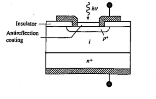
Figure: p-i-n photodiode Cross section.
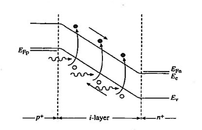
Figure: p-i-n photodiode Reverse bias energy band diagram.
It should also be noted than the heavy doping of the outer p and n regions causes the depletion means the minority carriers diffusion lengths in these regions will be relatively small. Asa result, the greater part of the photocurrent flowing in a p-i-n photodiode arises from carriers generated in the central depletion region.
Operational advantages of the p-i-n photodiode that have made it one of the most widely employed photodetectors stem, from the existences and tailor ability of the i-region.
For one, the diode con be optimized for response at a given wavelength by making the layer width equal to the inverse of the absorption coefficient (1/ ) of the specified wavelength Second, with one of the most photocurrent arising from light absorption to the i-region. Frequency response is greatly enhanced over that of a pn junction photodiode. The large ‘ξ-field is the depleted i-region leads to the rapid collection of photo generated carriers and a maximum frequency response.

Where WI is the width of the I region
Vsat is the saturation drift velocity
If WI = 5 then fmax =20GHz
The WI cannot be made arbitrary small to improve frequency.
The RC time constant associated with the internal series resistance (Rs)and the junction capacitance (CJ = Ks 0A/ WI) increases with decreasing WI and eventually limits the response time of the diode.
The excellent frequency response of the p-i-n photodiode makes it important for use as the photo detector in optical fibre telecommunication.
Q16) Write short notes on avalanche photodiode?
A16) Avalanche Photodiode are specially constructed p-i-n, pn, or even metal-semiconductor photodiodes that are operated near the avalanche breakdown point. A standard Si avalanche photodiode configuration is shown in figure.
One obvious special structural feature is the guard ring around the junction periphery. As noted in junction curvature leads to early breakdown about the junction periphery. The guard ring minimization of defect creation during device processing are also required to achieve uniform breakdown across the face of the junction. The primary advantage of the avalanche photodiode is a photo-signal gain leading to improvement in the signal-to-noise (S/N) ratio.
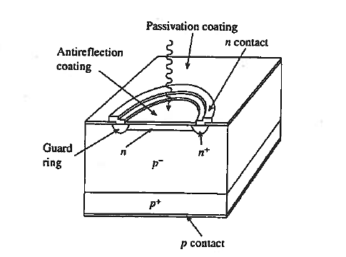
Figure: Avalanche Photodiode
As a general rule, amplification of signals is accompanied by amplification of the noise and added noise from the amplifier. Signal pain therefore typically loads to a reduction in the S/N ratio. Inside an avalanche photodiode, however, avalanche multiplication amplifies the photo-signal without amplifying the typically dominant receiver circuit noise. Thus there is an improvement in the S/N ratio until the added avalanche-related noise becomes comparable to the circuit noise.
Avalanche photodiodes made from lnGaAs on lnP and from Ge provide alternatives to the p-i-n photodiode for use in fiber optic telecommunication.
Q17) Explain CV characteristics of MOS transistors?
A17) The capacitance–voltage (C–V) measurement is a powerful and commonly used method of determining the gate oxide thickness, substrate doping concentration, threshold voltage, and flat-band voltage.
With d.c. Current flow blocked by the oxide, the major observable exhibited by MOS-Cs is capacitance. The varies as a function of the applied gate voltage.
To explain the observed farm of the C—V characteristics, let us consider how the charge inside an n-type MOS-C responds to the applied ac. Signal as the d.c. Bias is systematically changed from accumulation, through depletion, to inversion.
Accumulation: We know that accumulation with d.c. State is characterized by the pileup of majority carriers right at the oxide-semiconductor interface and state of the system can be changed very rapidly. Only majority carriers are involving in this process.
The device can follow the applied a.c. Signal quasi statically. Since the a.c. Signal merely adds or subtracts a charge close to the edges of an insulator, the small a.c. signal adding or subtracting a small Q on the two sides of the oxide as shown in Figure 6(a). Thus the charge configuration of charges inside MOS-C is similar ordinary parallel-plate capacitor.
For both low or high frequencies, we have
 ………..(1)
Where Ao is the area of the MOS-C gate.
Depletion: Under depletion biasing the d.c. Stale of an n-type MOS structure is characterized by a -Q charge on the gate and a +Q depletion layer charge in the semiconductor. The depletion layer charge is related the removal of majority
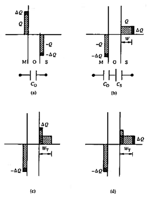
Figure: a.c. Charge fluctuation inside an n-type MOS-capacitor under d.c. biasing (a) accumulation (b) depletion, (c) inversion ( ), (d) inversion (
 )
)
Carriers from an effective width W adjacent to the oxide-semiconductor interface. State of the system can be changed very rapidly. Only majority carriers are involve in this process.
When the a c. Signal applied, it increases negative charge on the MOS-C gate and the width of depletion layer inside the semiconductor also increases then it starts fluctuating about its d.c. Value.
Now if the stationary d.c. Charge is conceptually eliminated. All that remains is a small fluctuating charge on the two sides of a double-layer insulator. For all frequencies this situation is clearly similar to two parallel plate capacitors (Co and Cs) in series, where

 ………..(2)
 ………..(3)
It is clear from equation (3) because W increases with increased depletion biasing, C(depl) correspondingly decreases as the d.c. bias is changed from flat band to the onset of inversion.
Inversion: Once inversion is achieved an appreciable number of minority carriers pile up near the oxide-semiconductor interface in response to the applied d.c. Bias. Also, the d.c. width of the depletion layer tends to maximize at WT. But the response to ac signal is not as quick.
The inversion layer charges fluctuate in response to the a.c. Signal. The observed charge fluctuation depends on the frequency of the at signal used in the capacitance measurement.
For low frequency(ω→0),

For high frequency (ω→)

We expect the MOS-C capacitance to be approximately constant at Co under accumulation biases, to decrease as the d.c. Bias progresses through depletion, and to be approximately constant again under inversion biases at a value equal to Co if ω→0 w 0 or C(depl)min, if ω→.
C-V characteristics shown in figure below
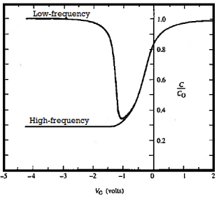
Figure: C-V Characteristics
Q18) Explain MOSFET as an amplifier?
A18) The purpose of amplifier is to amplify the weak signal faithfully. For amplification MOSFET should operate in a saturation region.
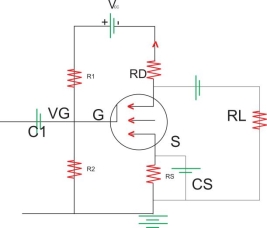
Figure: EMOSFET as an AMP
N-channel E-MOSFET Amp
- It can operate with positive gate and drain Vtg where as in p-channel with –ve gate and drain Vtg
- For amplification MOSFET should operate in saturation region where the drain current ID remains constant
- The threshold Vtg (VT) is the minimum gate Vtg (VGS) required to induce the channel between source to drain
- Fig shows single stage common source ampɤ using Vtg bias method
- Vin is A.c. Signal
- Resistors R1 ,R2 and R5 provides the proper and stabilized operating point
- C in i/p coupling capacitor where is coat is the o/p coupling capacitor which blocks the d.c signal
- Cs is the bypass capacitor so that signal available at source terminal. Never pass through Rs otherwise o/p Vtg reduces.
Q19) Draw and explain small signal model of CS MOS transistor?
A19) Common Source (CS) Amplifier
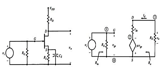
Fig: CS Amplifier and Small Signal equivalent Circuit
A simple Common Source amplifier and associated small signal equivalent circuit using voltage-source model of FET is shown in Figure above.
Voltage Gain
Source resistance (RS) is used to set the Q-Point but is bypassed by CS for mid-frequency operation. From the small signal equivalent circuit, the output voltage
VO = -RDµ Vgs (RD + rd)
Where Vgs = Vi,
The input voltage,
Hence, the voltage gain,
AV = VO / Vi = -RDµ (RD + rd)
Input Impedance
Zi = RG
For voltage divider bias as in CE Amplifiers of BJT
RG = R1 ║ R2
Output Impedance
Output impedance is the impedance measured at the output terminals with the input voltage VI = 0. When the input voltage Vi = 0, Vgs = 0
And hence µ Vgs = 0
The equivalent circuit for calculating output impedance is given in Figure below.
Output impedance
Zo = rd ║ RD
Normally rd will be far greater than RD. Hence Zo ≈ RD