Unit 2
High Frequency transistor models
- Explain the high-frequency transistor model?
Sol:
The high-frequency hybrid-π model for the BJT is given in Figure.
An additional terminal, B’, has been added to the schematic, and that resistance and capacitances have been defined between each pair of terminals.
The point denoted as B’ represents an internal base terminal that is not accessible to the outside world and that is separated by the physical base terminal, B, by a resistance denoted rbb’.
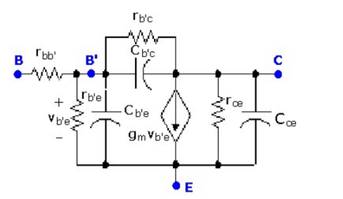
Figure. High-frequency model
 ≈ hie = (β+1) re ≈ β re
Gm ≈ 1/hib ≈ 1/re = β+1/hie ≈β/hie≈ Ic/VT
Ro ≈ 1/hoe = VA/IC
2. Explain the h parameters?
Sol:
The resistance related to h parameters are as follows :
Base spreading resistance:
The base spreading resistance models the equivalent resistance of silicon between the physical base terminal B and intrinsic terminal B’. The value of this resistance depends on the total current level and appears in the total input resistance as defined below.
Feedback resistance:
The feedback resistance models the effect of collector voltage on the base current.
Rb’c is at least equal βo ro where βo is the value of β at low frequencies and is typically on the order of 10βoro when the collector-base junction is reverse biased for normal active operational mode.
The feedback resistance is related to reverse voltage gain h-parameter hre through
Hre = v b’e/vce = r b’e/ rb’e + r b’c = r b’e/r b’c
Input resistance- the transistor input resistance between the base and emitter terminals and is indicated in the hybrid π model by rπ.The input resistance is approximately equal to the h parameter hie, where hie is defined as the input resistance of the device with short.
If we short the output of the circuit above and realize the base-collector junction is reverse biased so its resistance is much larger than the resistance associated with the forward-biased base-emitter junction.
Collector-junction capacitance Cb’c :
The collector junction capacitance is the capacitance of the collector-base junction. It is small with typical values in the range of 0.5 to 5pF although it varies with the width of the junction depletion region considered to be constant over a specific region of transistor operation.
CM1 = Cb’c (1-Av) input circuit
CM2 = Cb’c (1-1/A) output circuit
Output capacitance, Cce.
The output capacitance is defined between the collector and emitter terminals. It is usually extremely small and is generally ignored since the input capacitance is so much larger.
Base-emitter capacitance, Cb’e.
The base-emitter capacitance often called Cπ to associate it with rπ, is indicated in datasheets as Cib. This capacitance is the sum of two parts:
The emitter diffusion capacitance (Cde) is proportional to the dc bias current and an emitter junction depletion-layer capacitance (Cje) that is dependent on the value of base-emitter voltage, VBE, or
Cb’e = Cde + Cje
Since the first term is larger than the second, Cb’e is approximately equal to the diffusion capacitance
Cb’e = gm/2π fT re = |ICQ|/ 2π FT VT
Where fT is the unity gain frequency, a figure of merit defined as the frequency at which the common emitter short circuit current gain is 0 dB
Putting all this information together, we can present the high-frequency BJT equivalent circuit in terms of the familiar hybrid-π model as shown to the right and in Figure
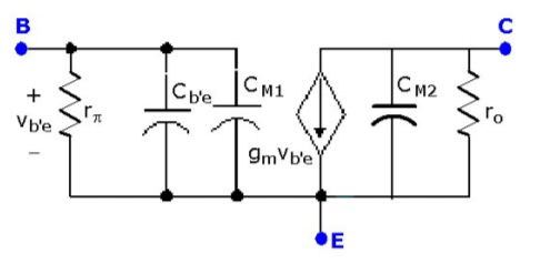
Figure. Equivalent high-frequency model
3. Explain the single-stage amplifier and its frequency response?
Sol:
Single-stage :
In the following circuit, a constant current biasing is selected, select the base resistance to be large to have large input resistance and at the same time limit the voltage drop across base resistance also, more importantly, the variability of this drop due to variations in the beta value for different transistors of the same type.
The dc voltage VB basically, determines the allowable signal swing at the collector.
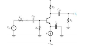
Figure. Single-stage CE Amplifier.

Figure. Frequency Response of CE amplifier
4. Explain the multistage amplifier and its frequency response?
Sol:
Multistage Amplifier:

Figure. Multistage Amplifier
A multistage amplifier design uses CE as the primary stage as well as CB as the second stage is named as a cascade amplifier.
Whenever the amplifier is cascaded, then it requires to employ a coupling network among o/p of one amplifier as well as i/p of the multistage amplifier. This kind of coupling is also named interstage coupling.
In this amplifier, there are three multistage amplifier types are used like RC coupling, transformer coupling, and direct coupling.
Frequency Response:
The gain’s phase-shift & amplifier’s voltage gain mainly depends on the range of frequency over the operation of the amplifier. Generally, the total range of frequency can be separated into 3-types like high-frequency range, mid-frequency, and low-frequency range
5. Explain cascode amplifier and its operation?
Sol:
The cascode amplifier is basically a two-stage amplifier in which the common-emitter stage is connected to the common base stage.
The CE-CB cascode connection is as shown in the figure:

Figure. Cascode Amplifier
When the input signal is applied at Q1 that is a common emitter stage and output is obtained at Q2.
Vcc, R1, R2, R3, Re are used to bias transistor Q1 and Q2 in the active region. Re is used to make Q-point stable against temperature variation.
The AC output voltage is obtained at the RC collector. The coupling capacitor is used to block dc signals which pass signals.
When the AC signal is applied at the base of Q1 it amplifies with unity gain, and voltage V01 appears across the collector of Q1. V01 acts as input to Q2 which further amplifies the signal and voltage Vo appears across the collector of CB Configuration.
To perform the small-signal analysis we need to draw ac equivalent circuit of the given amplifier.
To draw the ac equivalent circuit all the capacitors are replaced by a short circuit and the DC sources are connected to the ground.
The AC equivalent circuit is as shown in the figure:

Figure. AC equivalent model
The overall voltage gain is the product of the first stage gain to the second stage gain.
AVT = AV2 * AV1
AVT= (Vo/V1) * (V1/Vin)
From the above figure, we can see that Vo = Io*Rc......................................1
The output current is Io = hfb ie2
Hence substituting in equation 1 we get
Vo = hfb ie2 * Rc..................................................................................................2
To determine Vo1 we need to apply KVL to the input side of the common base connection
And we get Vo1 = ie2 * hib...........................................................................3
Divide equation 2 by 3 we get.
Vo/V1 =(hfb ie2 * Rc)/( ie2 * hib )
Av2 =(hfb * Rc)/(hib)...................................................................................4
Now determine the gain for the first stage,
Av1 = Vo1/Vin
From the above figure Vo1 = ie2 * hib...............................................................5
Since ie2 and hfe ib1 are opposite in direction,
We can write ie2 = -hfe *ib2
Substituting in above equation 5
Vo1 = -hfeib2 * hib....................6
To determine Vin we need to apply KVL at the input side.
Vin – hie ib1=0
Vin = hie ib1………..(7)
Now divide (6) and (7)
AV1= Vo1/Vin = (−hfe∗ib1)∗(hib*hie∗ib1)
AV1= −hfe∗(hib*hie)…………..(8)
But WE know
Hib=hie/(1+hfe)
Substitute in equation (8)
AV1= (−hfe/hie) ×( hie/1+hfe)
AV1= −hfe/(1+hfe)
AV1 ≈ -1 .......................9
Multiply AV1 and AV2 to obtain AVT
AVT= AV1×AV2
AVT= (−hfb∗Rc)/(hib).
The negative sign indicates the 180-degree phase shift provided by the CE stage.
Input impedance :
The input impedance is the parallel combination of resistors at the input side
Rin = R2 II R3 II hie.......................................................................................................10
Output Impedance :
The output impedance is given by the output resistance of the second stage
Ro = Rc....................................................................................................11
6. Explain the class A amplifier?
Sol:
Class A amplifier

Figure8. Class A amplifier
The Class A amplifier provides high linearity and low distortion. Here, the active elements that are the transistors are biased so their quiescent operating point is in the linear part of their conducting region.
The input signal induces small-to-moderate excursions around this point, thus maintaining the linearity of the input/output transfer function.
The active amplifier element is always on and never cut off, regardless of the magnitude or polarity of the input, as the Class A amplifier has a 360⁰ conduction angle, meaning it is on and conducts throughout a full cycle of the input sine.
The maximum theoretical efficiency that a class A amp can achieve is 50% efficiency with inductive output coupling or just 25% with capacitive coupling.
7. Explain the class B amplifier and its operation?
Sol:
Class B
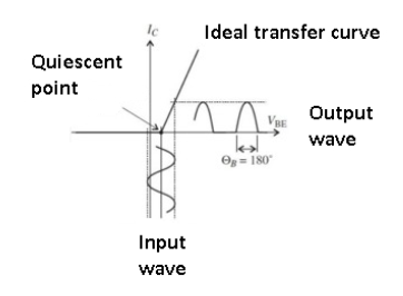
Figure. Class B amplifier
The Class B amplifier uses a “push-pull” arrangement with a pair of complementary amplifier elements (such as PNP/NPN transistors or N-/P-channel MOSFETs), each biased at cut-off with the conduction angle of each amplifier at 180⁰ (half cycle).
When the bipolar, zero-centered input signal goes positive, one amplifier comes out of cut-off and goes into its active region, conducts, and amplifies; when the signal goes negative, the other amplifier does the same while the first one is cut-off and thus dissipating near-zero power.
The Class B amplifier can have efficiency in the 30-40% range, far better than Class A although still unacceptably high for many applications.
It suffers from crossover distortion which generates harmonics, arising because of the slight lag or discontinuity as one active element turns on while the other turns off (and vice versa).
8. Explain the class AB amplifier and its operation?
Sol:
Class AB

Figure. Class AB amplifier
The Class AB amplifier is a blend of Class A and Class B.
Each of the pair of complementary active elements is biased slightly into the active region, and so there is some overlap between the two at the turn-on/turn-off center point as shown in the figure.
This reduces distortion to a low level – typically 1% and even down to 0.1% – at a slight increase in power dissipation. There is a trade-off between conduction angle, which is somewhat greater than 180⁰ which results in distortion with increased conduction angle and associated dissipation yielding lower distortion.
9. Explain the class C amplifier and its operation?
Sol:
Class C:

Figure 11. Class C amplifier
Though Class C amplifier offers the highest efficiency it has poor distortion qualities and generates many undesired harmonics.
In Class C, the amplifier conduction angle is far less than 180⁰, and it is biased so it only turns on for large signal excursions. The output current and thus dissipation is zero for more than one-half of the input signal.
The efficiency of Class C amplifiers is about 70-80%, but because the distortion is also high (10 to 30%) the Class C approach cannot be used for audio. However, it is used for higher-power RF transmitters, where dissipation must be kept to acceptably low levels.
10. Explain feedback topologies?
Sol:
- Voltage series
- Voltage shunt
- Current series
- Current shunt
Voltage-Series Feedback
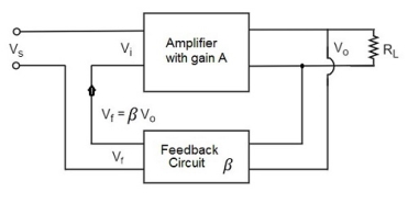
Figure. Voltage series feedback
In this type of circuit, a portion of the o/p voltage can be applied to the input voltage in series through the feedback circuit. The block diagram of the voltage series feedback-amplifier is shown below.
When the feedback circuit is allied in shunt through the output, then o/p impedance will be reduced and i/p impedance is enlarged because of the series connection with the input.
As the feedback circuit is connected in shunt with the output, the output impedance is decreased and due to the series connection with the input, the input impedance is increased.
Voltage-Shunt Feedback
In this type of circuit, a portion of the o/p voltage can be applied to the input voltage in parallel with the feedback circuit. The block diagram of the voltage shunt feedback-amplifier is shown below. When the feedback circuit is allied in shunt through the o/p as well as the input, then both the o/p impedance & the i/p impedance will be decreased.

Figure.Voltage shunt feedback
Current-Series Feedback
In this type of circuit, a portion of the o/p voltage is applied to the i/p voltage in series through the feedback circuit. The block diagram of the current series feedback-amplifier is shown below. When the feedback circuit is allied in series through the o/p as well as the input, then both the o/p impedance & the i/p impedance will be increased.

Figure. Current series
As the feedback circuit is connected in series with the output and the input as well, both the output impedance and the input impedance are increased.
Current-Shunt Feedback
In this type of circuit, a portion of the o/p voltage is applied to the i/p voltage in shunt through the feedback circuit. The block diagram of the current shunt feedback-amplifier is shown below.
When the feedback circuit is allied in series through the o/p in parallel with the input, then the o/p impedance will be increased & because of the parallel connection with the i/p, the i/p impedance will be decreased.
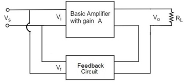
Figure: Current Shunt
As the feedback circuit is connected in series with the output, the output impedance is increased and due to the parallel connection with the input, the input impedance is decreased.
Effect of feedback gain and bandwidth
The transfer function is given by the equation:
M= A/(1- bA)
Hence the feedback reduces the overall gain of the system by a factor of (1-bA).
The quantities A and B are a function of frequency and can be adjusted to make the denominator greater than unity. Hence the gain increases for a particular frequency range and decreases for another frequency range.
Bandwidth is the parameter that measures the ability of the system to reproduce its input signal with high quality and the least noise. It is to be noted that the bandwidth increases with feedback.
11. Explain the gain and phase margin?
Sol:
The greater the Gain Margin (GM), the greater the stability of the system. The gain margin refers to the amount of gain, which can be increased or decreased without making the system unstable. It is usually expressed as a magnitude in dB.
This is done by calculating the vertical distance between the magnitude curve on the Bode magnitude plot and the x-axis at the frequency where the Bode phase plot = 180°. This point is known as the phase crossover frequency.
The formula for Gain Margin (GM) can be expressed as:
GM = 0 – G dB
Where G is the gain. This is the magnitude (in dB) as read from the vertical axis of the magnitude plot at the phase crossover frequency.
In our example shown in the graph above, the Gain (G) is 20. Hence using our formula for gain margin, the gain margin is equal to 0 – 20 dB = -20 dB which is unstable.
The greater the Phase Margin (PM), the greater will be the stability of the system. The phase margin refers to the amount of phase, which can be increased or decreased without making the system unstable. It is usually expressed as a phase in degrees.
This is done by calculating the vertical distance between the phase curve (on the Bode phase plot) and the x-axis at the frequency where the Bode magnitude plot = 0 dB. This point is known as the gain crossover frequency.
The formula for Phase Margin (PM) can be expressed as:
PM = ɸ - (-180)
Where ɸis the phase lag (a number less than 0). This is the phase as read from the vertical axis of the phase plot at the gain crossover frequency.
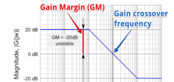
Figure Gain Margin

Figure. Phase Margin
Unit 2
Unit 2
High Frequency transistor models
- Explain the high-frequency transistor model?
Sol:
The high-frequency hybrid-π model for the BJT is given in Figure.
An additional terminal, B’, has been added to the schematic, and that resistance and capacitances have been defined between each pair of terminals.
The point denoted as B’ represents an internal base terminal that is not accessible to the outside world and that is separated by the physical base terminal, B, by a resistance denoted rbb’.

Figure. High-frequency model
 ≈ hie = (β+1) re ≈ β re
Gm ≈ 1/hib ≈ 1/re = β+1/hie ≈β/hie≈ Ic/VT
Ro ≈ 1/hoe = VA/IC
2. Explain the h parameters?
Sol:
The resistance related to h parameters are as follows :
Base spreading resistance:
The base spreading resistance models the equivalent resistance of silicon between the physical base terminal B and intrinsic terminal B’. The value of this resistance depends on the total current level and appears in the total input resistance as defined below.
Feedback resistance:
The feedback resistance models the effect of collector voltage on the base current.
Rb’c is at least equal βo ro where βo is the value of β at low frequencies and is typically on the order of 10βoro when the collector-base junction is reverse biased for normal active operational mode.
The feedback resistance is related to reverse voltage gain h-parameter hre through
Hre = v b’e/vce = r b’e/ rb’e + r b’c = r b’e/r b’c
Input resistance- the transistor input resistance between the base and emitter terminals and is indicated in the hybrid π model by rπ.The input resistance is approximately equal to the h parameter hie, where hie is defined as the input resistance of the device with short.
If we short the output of the circuit above and realize the base-collector junction is reverse biased so its resistance is much larger than the resistance associated with the forward-biased base-emitter junction.
Collector-junction capacitance Cb’c :
The collector junction capacitance is the capacitance of the collector-base junction. It is small with typical values in the range of 0.5 to 5pF although it varies with the width of the junction depletion region considered to be constant over a specific region of transistor operation.
CM1 = Cb’c (1-Av) input circuit
CM2 = Cb’c (1-1/A) output circuit
Output capacitance, Cce.
The output capacitance is defined between the collector and emitter terminals. It is usually extremely small and is generally ignored since the input capacitance is so much larger.
Base-emitter capacitance, Cb’e.
The base-emitter capacitance often called Cπ to associate it with rπ, is indicated in datasheets as Cib. This capacitance is the sum of two parts:
The emitter diffusion capacitance (Cde) is proportional to the dc bias current and an emitter junction depletion-layer capacitance (Cje) that is dependent on the value of base-emitter voltage, VBE, or
Cb’e = Cde + Cje
Since the first term is larger than the second, Cb’e is approximately equal to the diffusion capacitance
Cb’e = gm/2π fT re = |ICQ|/ 2π FT VT
Where fT is the unity gain frequency, a figure of merit defined as the frequency at which the common emitter short circuit current gain is 0 dB
Putting all this information together, we can present the high-frequency BJT equivalent circuit in terms of the familiar hybrid-π model as shown to the right and in Figure

Figure. Equivalent high-frequency model
3. Explain the single-stage amplifier and its frequency response?
Sol:
Single-stage :
In the following circuit, a constant current biasing is selected, select the base resistance to be large to have large input resistance and at the same time limit the voltage drop across base resistance also, more importantly, the variability of this drop due to variations in the beta value for different transistors of the same type.
The dc voltage VB basically, determines the allowable signal swing at the collector.

Figure. Single-stage CE Amplifier.

Figure. Frequency Response of CE amplifier
4. Explain the multistage amplifier and its frequency response?
Sol:
Multistage Amplifier:

Figure. Multistage Amplifier
A multistage amplifier design uses CE as the primary stage as well as CB as the second stage is named as a cascade amplifier.
Whenever the amplifier is cascaded, then it requires to employ a coupling network among o/p of one amplifier as well as i/p of the multistage amplifier. This kind of coupling is also named interstage coupling.
In this amplifier, there are three multistage amplifier types are used like RC coupling, transformer coupling, and direct coupling.
Frequency Response:
The gain’s phase-shift & amplifier’s voltage gain mainly depends on the range of frequency over the operation of the amplifier. Generally, the total range of frequency can be separated into 3-types like high-frequency range, mid-frequency, and low-frequency range
5. Explain cascode amplifier and its operation?
Sol:
The cascode amplifier is basically a two-stage amplifier in which the common-emitter stage is connected to the common base stage.
The CE-CB cascode connection is as shown in the figure:
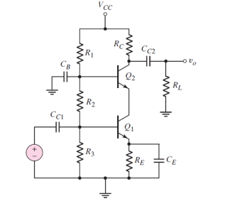
Figure. Cascode Amplifier
When the input signal is applied at Q1 that is a common emitter stage and output is obtained at Q2.
Vcc, R1, R2, R3, Re are used to bias transistor Q1 and Q2 in the active region. Re is used to make Q-point stable against temperature variation.
The AC output voltage is obtained at the RC collector. The coupling capacitor is used to block dc signals which pass signals.
When the AC signal is applied at the base of Q1 it amplifies with unity gain, and voltage V01 appears across the collector of Q1. V01 acts as input to Q2 which further amplifies the signal and voltage Vo appears across the collector of CB Configuration.
To perform the small-signal analysis we need to draw ac equivalent circuit of the given amplifier.
To draw the ac equivalent circuit all the capacitors are replaced by a short circuit and the DC sources are connected to the ground.
The AC equivalent circuit is as shown in the figure:

Figure. AC equivalent model
The overall voltage gain is the product of the first stage gain to the second stage gain.
AVT = AV2 * AV1
AVT= (Vo/V1) * (V1/Vin)
From the above figure, we can see that Vo = Io*Rc......................................1
The output current is Io = hfb ie2
Hence substituting in equation 1 we get
Vo = hfb ie2 * Rc..................................................................................................2
To determine Vo1 we need to apply KVL to the input side of the common base connection
And we get Vo1 = ie2 * hib...........................................................................3
Divide equation 2 by 3 we get.
Vo/V1 =(hfb ie2 * Rc)/( ie2 * hib )
Av2 =(hfb * Rc)/(hib)...................................................................................4
Now determine the gain for the first stage,
Av1 = Vo1/Vin
From the above figure Vo1 = ie2 * hib...............................................................5
Since ie2 and hfe ib1 are opposite in direction,
We can write ie2 = -hfe *ib2
Substituting in above equation 5
Vo1 = -hfeib2 * hib....................6
To determine Vin we need to apply KVL at the input side.
Vin – hie ib1=0
Vin = hie ib1………..(7)
Now divide (6) and (7)
AV1= Vo1/Vin = (−hfe∗ib1)∗(hib*hie∗ib1)
AV1= −hfe∗(hib*hie)…………..(8)
But WE know
Hib=hie/(1+hfe)
Substitute in equation (8)
AV1= (−hfe/hie) ×( hie/1+hfe)
AV1= −hfe/(1+hfe)
AV1 ≈ -1 .......................9
Multiply AV1 and AV2 to obtain AVT
AVT= AV1×AV2
AVT= (−hfb∗Rc)/(hib).
The negative sign indicates the 180-degree phase shift provided by the CE stage.
Input impedance :
The input impedance is the parallel combination of resistors at the input side
Rin = R2 II R3 II hie.......................................................................................................10
Output Impedance :
The output impedance is given by the output resistance of the second stage
Ro = Rc....................................................................................................11
6. Explain the class A amplifier?
Sol:
Class A amplifier

Figure8. Class A amplifier
The Class A amplifier provides high linearity and low distortion. Here, the active elements that are the transistors are biased so their quiescent operating point is in the linear part of their conducting region.
The input signal induces small-to-moderate excursions around this point, thus maintaining the linearity of the input/output transfer function.
The active amplifier element is always on and never cut off, regardless of the magnitude or polarity of the input, as the Class A amplifier has a 360⁰ conduction angle, meaning it is on and conducts throughout a full cycle of the input sine.
The maximum theoretical efficiency that a class A amp can achieve is 50% efficiency with inductive output coupling or just 25% with capacitive coupling.
7. Explain the class B amplifier and its operation?
Sol:
Class B

Figure. Class B amplifier
The Class B amplifier uses a “push-pull” arrangement with a pair of complementary amplifier elements (such as PNP/NPN transistors or N-/P-channel MOSFETs), each biased at cut-off with the conduction angle of each amplifier at 180⁰ (half cycle).
When the bipolar, zero-centered input signal goes positive, one amplifier comes out of cut-off and goes into its active region, conducts, and amplifies; when the signal goes negative, the other amplifier does the same while the first one is cut-off and thus dissipating near-zero power.
The Class B amplifier can have efficiency in the 30-40% range, far better than Class A although still unacceptably high for many applications.
It suffers from crossover distortion which generates harmonics, arising because of the slight lag or discontinuity as one active element turns on while the other turns off (and vice versa).
8. Explain the class AB amplifier and its operation?
Sol:
Class AB

Figure. Class AB amplifier
The Class AB amplifier is a blend of Class A and Class B.
Each of the pair of complementary active elements is biased slightly into the active region, and so there is some overlap between the two at the turn-on/turn-off center point as shown in the figure.
This reduces distortion to a low level – typically 1% and even down to 0.1% – at a slight increase in power dissipation. There is a trade-off between conduction angle, which is somewhat greater than 180⁰ which results in distortion with increased conduction angle and associated dissipation yielding lower distortion.
9. Explain the class C amplifier and its operation?
Sol:
Class C:
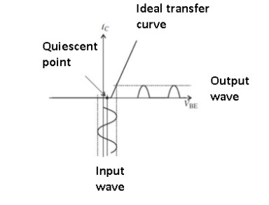
Figure 11. Class C amplifier
Though Class C amplifier offers the highest efficiency it has poor distortion qualities and generates many undesired harmonics.
In Class C, the amplifier conduction angle is far less than 180⁰, and it is biased so it only turns on for large signal excursions. The output current and thus dissipation is zero for more than one-half of the input signal.
The efficiency of Class C amplifiers is about 70-80%, but because the distortion is also high (10 to 30%) the Class C approach cannot be used for audio. However, it is used for higher-power RF transmitters, where dissipation must be kept to acceptably low levels.
10. Explain feedback topologies?
Sol:
- Voltage series
- Voltage shunt
- Current series
- Current shunt
Voltage-Series Feedback

Figure. Voltage series feedback
In this type of circuit, a portion of the o/p voltage can be applied to the input voltage in series through the feedback circuit. The block diagram of the voltage series feedback-amplifier is shown below.
When the feedback circuit is allied in shunt through the output, then o/p impedance will be reduced and i/p impedance is enlarged because of the series connection with the input.
As the feedback circuit is connected in shunt with the output, the output impedance is decreased and due to the series connection with the input, the input impedance is increased.
Voltage-Shunt Feedback
In this type of circuit, a portion of the o/p voltage can be applied to the input voltage in parallel with the feedback circuit. The block diagram of the voltage shunt feedback-amplifier is shown below. When the feedback circuit is allied in shunt through the o/p as well as the input, then both the o/p impedance & the i/p impedance will be decreased.
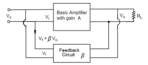
Figure.Voltage shunt feedback
Current-Series Feedback
In this type of circuit, a portion of the o/p voltage is applied to the i/p voltage in series through the feedback circuit. The block diagram of the current series feedback-amplifier is shown below. When the feedback circuit is allied in series through the o/p as well as the input, then both the o/p impedance & the i/p impedance will be increased.

Figure. Current series
As the feedback circuit is connected in series with the output and the input as well, both the output impedance and the input impedance are increased.
Current-Shunt Feedback
In this type of circuit, a portion of the o/p voltage is applied to the i/p voltage in shunt through the feedback circuit. The block diagram of the current shunt feedback-amplifier is shown below.
When the feedback circuit is allied in series through the o/p in parallel with the input, then the o/p impedance will be increased & because of the parallel connection with the i/p, the i/p impedance will be decreased.

Figure: Current Shunt
As the feedback circuit is connected in series with the output, the output impedance is increased and due to the parallel connection with the input, the input impedance is decreased.
Effect of feedback gain and bandwidth
The transfer function is given by the equation:
M= A/(1- bA)
Hence the feedback reduces the overall gain of the system by a factor of (1-bA).
The quantities A and B are a function of frequency and can be adjusted to make the denominator greater than unity. Hence the gain increases for a particular frequency range and decreases for another frequency range.
Bandwidth is the parameter that measures the ability of the system to reproduce its input signal with high quality and the least noise. It is to be noted that the bandwidth increases with feedback.
11. Explain the gain and phase margin?
Sol:
The greater the Gain Margin (GM), the greater the stability of the system. The gain margin refers to the amount of gain, which can be increased or decreased without making the system unstable. It is usually expressed as a magnitude in dB.
This is done by calculating the vertical distance between the magnitude curve on the Bode magnitude plot and the x-axis at the frequency where the Bode phase plot = 180°. This point is known as the phase crossover frequency.
The formula for Gain Margin (GM) can be expressed as:
GM = 0 – G dB
Where G is the gain. This is the magnitude (in dB) as read from the vertical axis of the magnitude plot at the phase crossover frequency.
In our example shown in the graph above, the Gain (G) is 20. Hence using our formula for gain margin, the gain margin is equal to 0 – 20 dB = -20 dB which is unstable.
The greater the Phase Margin (PM), the greater will be the stability of the system. The phase margin refers to the amount of phase, which can be increased or decreased without making the system unstable. It is usually expressed as a phase in degrees.
This is done by calculating the vertical distance between the phase curve (on the Bode phase plot) and the x-axis at the frequency where the Bode magnitude plot = 0 dB. This point is known as the gain crossover frequency.
The formula for Phase Margin (PM) can be expressed as:
PM = ɸ - (-180)
Where ɸis the phase lag (a number less than 0). This is the phase as read from the vertical axis of the phase plot at the gain crossover frequency.

Figure Gain Margin

Figure. Phase Margin
Unit 2
High Frequency transistor models
- Explain the high-frequency transistor model?
Sol:
The high-frequency hybrid-π model for the BJT is given in Figure.
An additional terminal, B’, has been added to the schematic, and that resistance and capacitances have been defined between each pair of terminals.
The point denoted as B’ represents an internal base terminal that is not accessible to the outside world and that is separated by the physical base terminal, B, by a resistance denoted rbb’.

Figure. High-frequency model
 ≈ hie = (β+1) re ≈ β re
Gm ≈ 1/hib ≈ 1/re = β+1/hie ≈β/hie≈ Ic/VT
Ro ≈ 1/hoe = VA/IC
2. Explain the h parameters?
Sol:
The resistance related to h parameters are as follows :
Base spreading resistance:
The base spreading resistance models the equivalent resistance of silicon between the physical base terminal B and intrinsic terminal B’. The value of this resistance depends on the total current level and appears in the total input resistance as defined below.
Feedback resistance:
The feedback resistance models the effect of collector voltage on the base current.
Rb’c is at least equal βo ro where βo is the value of β at low frequencies and is typically on the order of 10βoro when the collector-base junction is reverse biased for normal active operational mode.
The feedback resistance is related to reverse voltage gain h-parameter hre through
Hre = v b’e/vce = r b’e/ rb’e + r b’c = r b’e/r b’c
Input resistance- the transistor input resistance between the base and emitter terminals and is indicated in the hybrid π model by rπ.The input resistance is approximately equal to the h parameter hie, where hie is defined as the input resistance of the device with short.
If we short the output of the circuit above and realize the base-collector junction is reverse biased so its resistance is much larger than the resistance associated with the forward-biased base-emitter junction.
Collector-junction capacitance Cb’c :
The collector junction capacitance is the capacitance of the collector-base junction. It is small with typical values in the range of 0.5 to 5pF although it varies with the width of the junction depletion region considered to be constant over a specific region of transistor operation.
CM1 = Cb’c (1-Av) input circuit
CM2 = Cb’c (1-1/A) output circuit
Output capacitance, Cce.
The output capacitance is defined between the collector and emitter terminals. It is usually extremely small and is generally ignored since the input capacitance is so much larger.
Base-emitter capacitance, Cb’e.
The base-emitter capacitance often called Cπ to associate it with rπ, is indicated in datasheets as Cib. This capacitance is the sum of two parts:
The emitter diffusion capacitance (Cde) is proportional to the dc bias current and an emitter junction depletion-layer capacitance (Cje) that is dependent on the value of base-emitter voltage, VBE, or
Cb’e = Cde + Cje
Since the first term is larger than the second, Cb’e is approximately equal to the diffusion capacitance
Cb’e = gm/2π fT re = |ICQ|/ 2π FT VT
Where fT is the unity gain frequency, a figure of merit defined as the frequency at which the common emitter short circuit current gain is 0 dB
Putting all this information together, we can present the high-frequency BJT equivalent circuit in terms of the familiar hybrid-π model as shown to the right and in Figure

Figure. Equivalent high-frequency model
3. Explain the single-stage amplifier and its frequency response?
Sol:
Single-stage :
In the following circuit, a constant current biasing is selected, select the base resistance to be large to have large input resistance and at the same time limit the voltage drop across base resistance also, more importantly, the variability of this drop due to variations in the beta value for different transistors of the same type.
The dc voltage VB basically, determines the allowable signal swing at the collector.

Figure. Single-stage CE Amplifier.
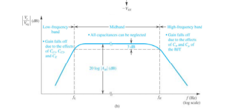
Figure. Frequency Response of CE amplifier
4. Explain the multistage amplifier and its frequency response?
Sol:
Multistage Amplifier:

Figure. Multistage Amplifier
A multistage amplifier design uses CE as the primary stage as well as CB as the second stage is named as a cascade amplifier.
Whenever the amplifier is cascaded, then it requires to employ a coupling network among o/p of one amplifier as well as i/p of the multistage amplifier. This kind of coupling is also named interstage coupling.
In this amplifier, there are three multistage amplifier types are used like RC coupling, transformer coupling, and direct coupling.
Frequency Response:
The gain’s phase-shift & amplifier’s voltage gain mainly depends on the range of frequency over the operation of the amplifier. Generally, the total range of frequency can be separated into 3-types like high-frequency range, mid-frequency, and low-frequency range
5. Explain cascode amplifier and its operation?
Sol:
The cascode amplifier is basically a two-stage amplifier in which the common-emitter stage is connected to the common base stage.
The CE-CB cascode connection is as shown in the figure:

Figure. Cascode Amplifier
When the input signal is applied at Q1 that is a common emitter stage and output is obtained at Q2.
Vcc, R1, R2, R3, Re are used to bias transistor Q1 and Q2 in the active region. Re is used to make Q-point stable against temperature variation.
The AC output voltage is obtained at the RC collector. The coupling capacitor is used to block dc signals which pass signals.
When the AC signal is applied at the base of Q1 it amplifies with unity gain, and voltage V01 appears across the collector of Q1. V01 acts as input to Q2 which further amplifies the signal and voltage Vo appears across the collector of CB Configuration.
To perform the small-signal analysis we need to draw ac equivalent circuit of the given amplifier.
To draw the ac equivalent circuit all the capacitors are replaced by a short circuit and the DC sources are connected to the ground.
The AC equivalent circuit is as shown in the figure:

Figure. AC equivalent model
The overall voltage gain is the product of the first stage gain to the second stage gain.
AVT = AV2 * AV1
AVT= (Vo/V1) * (V1/Vin)
From the above figure, we can see that Vo = Io*Rc......................................1
The output current is Io = hfb ie2
Hence substituting in equation 1 we get
Vo = hfb ie2 * Rc..................................................................................................2
To determine Vo1 we need to apply KVL to the input side of the common base connection
And we get Vo1 = ie2 * hib...........................................................................3
Divide equation 2 by 3 we get.
Vo/V1 =(hfb ie2 * Rc)/( ie2 * hib )
Av2 =(hfb * Rc)/(hib)...................................................................................4
Now determine the gain for the first stage,
Av1 = Vo1/Vin
From the above figure Vo1 = ie2 * hib...............................................................5
Since ie2 and hfe ib1 are opposite in direction,
We can write ie2 = -hfe *ib2
Substituting in above equation 5
Vo1 = -hfeib2 * hib....................6
To determine Vin we need to apply KVL at the input side.
Vin – hie ib1=0
Vin = hie ib1………..(7)
Now divide (6) and (7)
AV1= Vo1/Vin = (−hfe∗ib1)∗(hib*hie∗ib1)
AV1= −hfe∗(hib*hie)…………..(8)
But WE know
Hib=hie/(1+hfe)
Substitute in equation (8)
AV1= (−hfe/hie) ×( hie/1+hfe)
AV1= −hfe/(1+hfe)
AV1 ≈ -1 .......................9
Multiply AV1 and AV2 to obtain AVT
AVT= AV1×AV2
AVT= (−hfb∗Rc)/(hib).
The negative sign indicates the 180-degree phase shift provided by the CE stage.
Input impedance :
The input impedance is the parallel combination of resistors at the input side
Rin = R2 II R3 II hie.......................................................................................................10
Output Impedance :
The output impedance is given by the output resistance of the second stage
Ro = Rc....................................................................................................11
6. Explain the class A amplifier?
Sol:
Class A amplifier
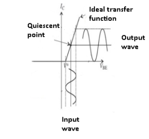
Figure8. Class A amplifier
The Class A amplifier provides high linearity and low distortion. Here, the active elements that are the transistors are biased so their quiescent operating point is in the linear part of their conducting region.
The input signal induces small-to-moderate excursions around this point, thus maintaining the linearity of the input/output transfer function.
The active amplifier element is always on and never cut off, regardless of the magnitude or polarity of the input, as the Class A amplifier has a 360⁰ conduction angle, meaning it is on and conducts throughout a full cycle of the input sine.
The maximum theoretical efficiency that a class A amp can achieve is 50% efficiency with inductive output coupling or just 25% with capacitive coupling.
7. Explain the class B amplifier and its operation?
Sol:
Class B

Figure. Class B amplifier
The Class B amplifier uses a “push-pull” arrangement with a pair of complementary amplifier elements (such as PNP/NPN transistors or N-/P-channel MOSFETs), each biased at cut-off with the conduction angle of each amplifier at 180⁰ (half cycle).
When the bipolar, zero-centered input signal goes positive, one amplifier comes out of cut-off and goes into its active region, conducts, and amplifies; when the signal goes negative, the other amplifier does the same while the first one is cut-off and thus dissipating near-zero power.
The Class B amplifier can have efficiency in the 30-40% range, far better than Class A although still unacceptably high for many applications.
It suffers from crossover distortion which generates harmonics, arising because of the slight lag or discontinuity as one active element turns on while the other turns off (and vice versa).
8. Explain the class AB amplifier and its operation?
Sol:
Class AB
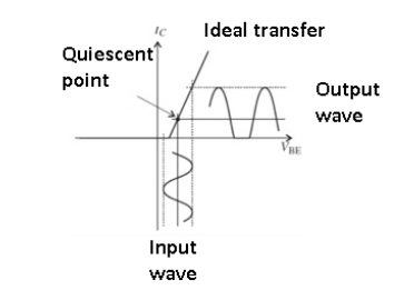
Figure. Class AB amplifier
The Class AB amplifier is a blend of Class A and Class B.
Each of the pair of complementary active elements is biased slightly into the active region, and so there is some overlap between the two at the turn-on/turn-off center point as shown in the figure.
This reduces distortion to a low level – typically 1% and even down to 0.1% – at a slight increase in power dissipation. There is a trade-off between conduction angle, which is somewhat greater than 180⁰ which results in distortion with increased conduction angle and associated dissipation yielding lower distortion.
9. Explain the class C amplifier and its operation?
Sol:
Class C:

Figure 11. Class C amplifier
Though Class C amplifier offers the highest efficiency it has poor distortion qualities and generates many undesired harmonics.
In Class C, the amplifier conduction angle is far less than 180⁰, and it is biased so it only turns on for large signal excursions. The output current and thus dissipation is zero for more than one-half of the input signal.
The efficiency of Class C amplifiers is about 70-80%, but because the distortion is also high (10 to 30%) the Class C approach cannot be used for audio. However, it is used for higher-power RF transmitters, where dissipation must be kept to acceptably low levels.
10. Explain feedback topologies?
Sol:
- Voltage series
- Voltage shunt
- Current series
- Current shunt
Voltage-Series Feedback

Figure. Voltage series feedback
In this type of circuit, a portion of the o/p voltage can be applied to the input voltage in series through the feedback circuit. The block diagram of the voltage series feedback-amplifier is shown below.
When the feedback circuit is allied in shunt through the output, then o/p impedance will be reduced and i/p impedance is enlarged because of the series connection with the input.
As the feedback circuit is connected in shunt with the output, the output impedance is decreased and due to the series connection with the input, the input impedance is increased.
Voltage-Shunt Feedback
In this type of circuit, a portion of the o/p voltage can be applied to the input voltage in parallel with the feedback circuit. The block diagram of the voltage shunt feedback-amplifier is shown below. When the feedback circuit is allied in shunt through the o/p as well as the input, then both the o/p impedance & the i/p impedance will be decreased.

Figure.Voltage shunt feedback
Current-Series Feedback
In this type of circuit, a portion of the o/p voltage is applied to the i/p voltage in series through the feedback circuit. The block diagram of the current series feedback-amplifier is shown below. When the feedback circuit is allied in series through the o/p as well as the input, then both the o/p impedance & the i/p impedance will be increased.
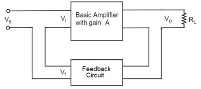
Figure. Current series
As the feedback circuit is connected in series with the output and the input as well, both the output impedance and the input impedance are increased.
Current-Shunt Feedback
In this type of circuit, a portion of the o/p voltage is applied to the i/p voltage in shunt through the feedback circuit. The block diagram of the current shunt feedback-amplifier is shown below.
When the feedback circuit is allied in series through the o/p in parallel with the input, then the o/p impedance will be increased & because of the parallel connection with the i/p, the i/p impedance will be decreased.

Figure: Current Shunt
As the feedback circuit is connected in series with the output, the output impedance is increased and due to the parallel connection with the input, the input impedance is decreased.
Effect of feedback gain and bandwidth
The transfer function is given by the equation:
M= A/(1- bA)
Hence the feedback reduces the overall gain of the system by a factor of (1-bA).
The quantities A and B are a function of frequency and can be adjusted to make the denominator greater than unity. Hence the gain increases for a particular frequency range and decreases for another frequency range.
Bandwidth is the parameter that measures the ability of the system to reproduce its input signal with high quality and the least noise. It is to be noted that the bandwidth increases with feedback.
11. Explain the gain and phase margin?
Sol:
The greater the Gain Margin (GM), the greater the stability of the system. The gain margin refers to the amount of gain, which can be increased or decreased without making the system unstable. It is usually expressed as a magnitude in dB.
This is done by calculating the vertical distance between the magnitude curve on the Bode magnitude plot and the x-axis at the frequency where the Bode phase plot = 180°. This point is known as the phase crossover frequency.
The formula for Gain Margin (GM) can be expressed as:
GM = 0 – G dB
Where G is the gain. This is the magnitude (in dB) as read from the vertical axis of the magnitude plot at the phase crossover frequency.
In our example shown in the graph above, the Gain (G) is 20. Hence using our formula for gain margin, the gain margin is equal to 0 – 20 dB = -20 dB which is unstable.
The greater the Phase Margin (PM), the greater will be the stability of the system. The phase margin refers to the amount of phase, which can be increased or decreased without making the system unstable. It is usually expressed as a phase in degrees.
This is done by calculating the vertical distance between the phase curve (on the Bode phase plot) and the x-axis at the frequency where the Bode magnitude plot = 0 dB. This point is known as the gain crossover frequency.
The formula for Phase Margin (PM) can be expressed as:
PM = ɸ - (-180)
Where ɸis the phase lag (a number less than 0). This is the phase as read from the vertical axis of the phase plot at the gain crossover frequency.

Figure Gain Margin
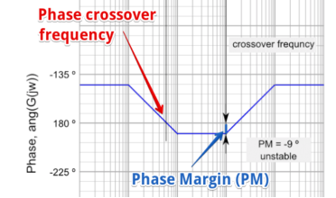
Figure. Phase Margin