Unit - 3
16-bit Microprocessors (8086) and Peripheral Devices
Q1) Explain the architecture of 8086?
A1)
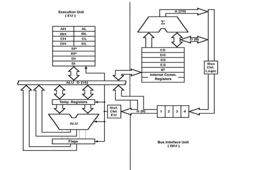
8086, it is a 16-bit Integer processor in a 40 pin, Dual Inline Packaged IC.
The size of the internal registers indicates how much information the processor can operate on at a time and how it moves data around internally within the chip, sometimes also referred to as the internal data bus.
8086 provides the programmer with 14 internal registers, each 16 bits or 2 Bytes wide.
8086 has two blocks BIU and EU. • The BIU handles all transactions of data and addresses on the buses for EU. • The BIU performs all bus operations such as instruction fetching, reading and writing operands for memory and calculating the addresses of the memory operands. The instruction bytes are transferred to the instruction queue. • EU executes instructions from the instruction system byte queue.
BIU contains Instruction queue, Segment registers, Instruction pointer, Address adder. • EU contains Control circuitry, Instruction decoder, ALU, Pointer and Index register, Flag register.
Decodes instructions fetched by the BIU • Generate control signals, • Executes instructions
The main parts are: • Control Circuitry • Instruction decoder • ALU
General Purpose Registers
AX: AH AL
BX:BH BL
CX:CH CL
DX: DH DL
SP: Stack Pointer
BP: Base Pointer
SI DI Source Index Destination Index
Pointer And Index Registers
• used to keep offset addresses.
• Used in various forms of memory addressing.
• In the case of SP and BP the default reference to form a physical address is the Stack Segment
• The index registers (SI & DI) and the BX generally default to the Data segment register (DS).
SP: Stack pointer – Used with SS to access the stack segment
BP: Base Pointer – Primarily used to access data on the stack – Can be used to access data in other segments
• SI: Source Index register – is required for some string operations – When string operations are performed, the SI register points to memory locations in the data segment which is addressed by the DS register. Thus, SI is associated with the DS in string operations.
• DI: Destination Index register – is also required for some string operations. – When string operations are performed, the DI register points to memory locations in the data segment which is addressed by the ES register. Thus, DI is associated with the ES in string operations.
• The SI and the DI registers may also be used to access data stored in arrays
Q2) Explain the pin diagram of 8086?
A2)
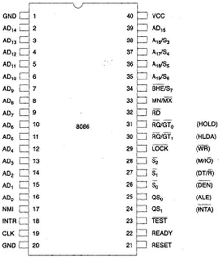
Power supply and frequency signals
It uses 5V DC supply at VCC pin 40, and uses ground at VSS pin 1 and 20 for its operation.
Clock signal
Clock signal is provided through Pin-19. It provides timing to the processor for operations. Its frequency is different for different versions, i.e., 5MHz, 8MHz and 10MHz.
Address/data bus
AD0-AD15. These are 16 address/data bus. AD0-AD7 carries low order byte data and AD8AD15 carries higher order byte data. During the first clock cycle, it carries 16-bit address and after that it carries 16-bit data.
Address/status bus
A16-A19/S3-S6. These are the 4 address/status buses. During the first clock cycle, it carries 4-bit address and later it carries status signals.
S7/BHE
BHE stands for Bus High Enable. It is available at pin 34 and used to indicate the transfer of data using data bus D8-D15. This signal is low during the first clock cycle, thereafter it is active.
Read
It is available at pin 32 and is used to read signal for Read operation.
Ready
It is available at pin 22. It is an acknowledgement signal from I/O devices that data is transferred. It is an active high signal. When it is high, it indicates that the device is ready to transfer data. When it is low, it indicates wait state.
RESET
It is available at pin 21 and is used to restart the execution. It causes the processor to immediately terminate its present activity. This signal is active high for the first 4 clock cycles to RESET the microprocessor.
INTR
It is available at pin 18. It is an interrupt request signal, which is sampled during the last clock cycle of each instruction to determine if the processor considered this as an interrupt or not.
NMI
It stands for non-maskable interrupt and is available at pin 17. It is an edge triggered input, which causes an interrupt request to the microprocessor.
This signal is like wait state and is available at pin 23. When this signal is high, then the processor has to wait for IDLE state, else the execution continues.
MN/MX
It stands for Minimum/Maximum and is available at pin 33. It indicates what mode the processor is to operate in; when it is high, it works in the minimum mode and vice-versa.
INTA
It is an interrupt acknowledgement signal and id available at pin 24. When the microprocessor receives this signal, it acknowledges the interrupt.
ALE
It stands for address enable latch and is available at pin 25. A positive pulse is generated each time the processor begins any operation. This signal indicates the availability of a valid address on the address/data lines.
DEN
It stands for Data Enable and is available at pin 26. It is used to enable Trans receiver 8286. The trans receiver is a device used to separate data from the address/data bus.
DT/R
It stands for Data Transmit/Receive signal and is available at pin 27. It decides the direction of data flow through the trans receiver. When it is high, data is transmitted out and vice-a-versa.
M/IO
This signal is used to distinguish between memory and I/O operations. When it is high, it indicates I/O operation and when it is low indicates the memory operation. It is available at pin 28.
WR
It stands for write signal and is available at pin 29. It is used to write the data into the memory or the output device depending on the status of M/IO signal.
HLDA
It stands for Hold Acknowledgement signal and is available at pin 30. This signal acknowledges the HOLD signal.
HOLD
This signal indicates to the processor that external devices are requesting to access the address/data buses. It is available at pin 31.
QS1 and QS0
These are queue status signals and are available at pin 24 and 25. These signals provide the status of instruction queue. Their conditions are shown in the following table −
QS0 | QS1 | Status |
0 | 0 | No operation |
0 | 1 | First byte of opcode from the queue |
1 | 0 | Empty the queue |
1 | 1 | Subsequent byte from the queue |
S0, S1, S2
These are the status signals that provide the status of operation, which is used by the Bus Controller 8288 to generate memory & I/O control signals. These are available at pin 26, 27, and 28. Following is the table showing their status −
S2 | S1 | S0 | Status |
0 | 0 | 0 | Interrupt acknowledgement |
0 | 0 | 1 | I/O Read |
0 | 1 | 0 | I/O Write |
0 | 1 | 1 | Halt |
1 | 0 | 0 | Opcode fetch |
1 | 0 | 1 | Memory read |
1 | 1 | 0 | Memory write |
1 | 1 | 1 | Passive |
LOCK
When this signal is active, it indicates to the other processors not to ask the CPU to leave the system bus. It is activated using the LOCK prefix on any instruction and is available at pin 29.
RQ/GT1 and RQ/GT0
These are the Request/Grant signals used by the other processors requesting the CPU to release the system bus. When the signal is received by CPU, then it sends acknowledgment. RQ/GT0 has a higher priority than RQ/GT1.
Q3) Explain the generation of physical address?
A3)
Address Generation Circuit:
- The BIU has a Physical Address Generation Circuit.
- It generates the 20- bit physical address using Segment and Offset addresses using the formula:
- Physical Address = Segment Address + Offset Address
Q4) Explain memory fragmentation?
A4)
The size of address bus of 8086 is 20 and is able to address 1 Mbytes ( ) of physical memory, but all this memory is not active at one time. Actually, this 1Mbytes of memory are partitioned into 16 parts named as segments. Size of each segment is 64Kbytes (65,536).
Only four of these segments are active at a time:
- Code segment holds the program instruction codes
- Stack segment is used to store interrupt and subroutine return addresses
- Data segment stores data for the program
- Extra segment is an extra data segment (often used for shared data)
- Each of these segments are addressed by an address stored in corresponding segment registers: CS (code segment), SS (stack segment), DS (data segment), and ES (extra segment). These registers contain a 16-bit base address that points to the lowest addressed byte of the segment. Because the segment registers cannot store 20 bits, they only store the upper 16 bits. The BIU takes care of this problem by appending four 0's to the low-order bits of the segment register. In effect, this multiplies the segment register contents by 16.
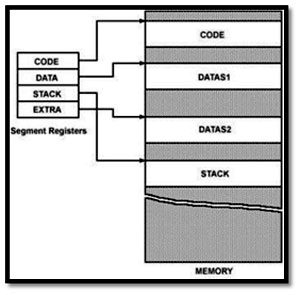
The segment registers are user accessible, which means that the programmer can change the content of segment registers through software.
Q5) Explain memory organization?
A5)
8086 is 16-bit processor that can supports 1Mbyte (i.e., 20-bit address bus: 220) of external memory over the address range 0000016 to FFFFF16. The 8086 organizes memory as individual bytes of data. The 8086 can access any two consecutive bytes as a word of data. The lower-addressed byte is the least significant byte of the word, and the higher- addressed byte is its most significant byte.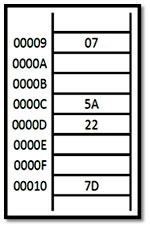
Part of 1 Mbyte Memory
The above figure represents:
Storage location of address 0000916 contains the value 716, while the location of address 0001016 contains the value 7D16.
The 16-bit word 225A16is stored in the locations 0000C16 to 0000D16
The word of data is at an even-address boundary (i.e., address of least significant byte is even) is called aligned word.
The word of data is at an odd-address boundary is called misaligned word, as shown in Figure below.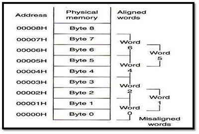
Figure: Aligned and misaligned word
To store double word four locations are needed. The double word that it’s least significant byte address is a multiple of 4 (e.g., 0 16, 416, 816 ...) is called aligned double word. The double word at address of non-multiples of 4 is called misaligned double word shown in Figure below.
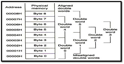
Figure: Aligned and misaligned double word
Q6) Explain the addressing modes?
A6)
Types of addressing modes:
Register mode – In this type of addressing mode both the operands are registers.
Example:
MOV AX, BX
XOR AX, DX
ADD AL, BL
Immediate mode – In this type of addressing mode the source operand is a 8 bit or 16-bit data. Destination operand can never be immediate data.
Example:
MOV AX, 2000
MOV CL, 0A
ADD AL, 45
AND AX, 0000
MOV AX, 2000
MOV CS, AX
Displacement or direct mode – In this type of addressing mode the effective address is directly given in the instruction as displacement.
Example:
MOV AX, [DISP]
MOV AX, [0500]
Register indirect mode – In this addressing mode the effective address is in SI, DI or BX.
Example:
MOV AX, [DI]
ADD AL, [BX]
MOV AX, [SI]
Based indexed mode – In this the effective address is sum of base register and index register.
Base register: BX, BP
Index register: SI, DI
The physical memory address is calculated according to the base register.
Example:
MOV AL, [BP+SI]
MOV AX, [BX+DI]
Indexed mode – In this type of addressing mode the effective address is sum of index register and displacement.
Example:
MOV AX, [SI+2000]
MOV AL, [DI+3000]
Based mode – In this the effective address is the sum of base register and displacement.
Example:
MOV AL, [BP+ 0100]
Based indexed displacement mode – In this type of addressing mode the effective address is the sum of index register, base register and displacement.
Example:
MOV AL, [SI+BP+2000]
String mode – This addressing mode is related to string instructions. In this the value of SI and DI are auto incremented and decremented depending upon the value of directional flag.
Example:
MOVS B
MOVS W
Input/Output mode – This addressing mode is related with input output operations.
Example:
IN A, 45
OUT A, 50
Relative mode –
In this the effective address is calculated with reference to instruction pointer.
Example:
JNZ 8 bit address
IP=IP+8 bit address
Q6) Explain 8237 DMA controller pin diagram?
A6)
Pin Configuration
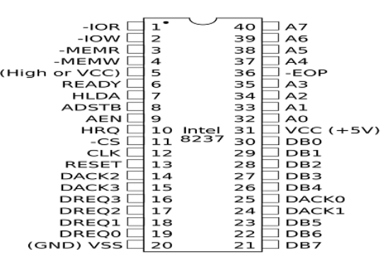
Fig.: Pin Configuration of 8237
- It uses a power supply of 5V.
- D7-0 / A15-8: For communicating, there are 8 bidirectional data pins. When the processor is in active mode and the 8257 in active state then it is in slave mode. When the processor remains in the HOLD state and 8257 behaves as the master, then they send most significant 8 bits of memory address.
- A3-0: When the processor remains in active state and uses address input pins of 8257 to select one of the registers.
- IOR: It is an active low signal which is activated by the processor to read an Address Register, Counter Register, or the status register, when the it works in the slave mode.
- IOW: It is an active low signal which is activated by the processor to write to an Address Register, Counter Register, or the control register, when the it remains in the slave mode.
- MR: It is an active low output pin which operates when it is in the slave mode.
- MW: It is an active low output pin when it is in the slave mode. When the processor is in the HOLD state, it drives the pin that is activated for a DMA write machine cycle and becomes inactive for DMA read machine cycle.
- CS: It is an active low input pin used for chip selection.
- CLK: It is an input pin for clock pulse. The maximum allowed frequency is about 3 MHz. The input of the clock is connected to the output of the processor in a system which is based on 8086.
- READY: It is an active high input pin. Devices having slow access times can use it to insert wait states during the DMA read or write to the machine cycles.
- HRQ: HRQ stands for HOLD REQUEST. It is an active high output pin and is connected to the HOLD input of 8086. Whenever a DRQ input inactive and the DMA channel corresponding to it is enabled then the HRQ output is activated by 8257.
- HLDA: HLDA stands for HOLD acknowledge. It is an active high input pin which is connected to the HLDA output of 8086.
- TC: TC stands for terminal count and is an active high output pin. The output is activated when all the 14 Least Significant bits of the Control Register becomes 0.
- MARK: This is an active high output pin and is activated when the Least Significant 7 bits of the Control Register become 0 for the DMA channel.
- AEN: AEN stands for address enable. It is an active high output pin. Intel8257 gives an output 0 on AEN when 8086 becomes the master of the computer system.
- ADSTB: ADSTB stands for address strobe and is an active high output pin performing the same function to output of 8085. Here, if the output on this pin is 0, then it is in the slave mode.
- DACK3-0: These are the active low DMA acknowledged output pins used only once for every four DMA channels.
- DRQ3-0: They are active high DMA request input pins assigned one for each DMA channel. They are activated by some special-purpose I/O port chips.
- RESET: It is an active high input pin which is connected to the RESET-OUT pin of 8086. After 8257 is reset, the control register contents turn to 00H.
Q7) Explain the functional diagram?
A7)
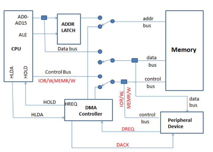
Fig. Functional Block Diagram of 8237
- The 8237 supplies memory & I/O with control signals and memory address information during the DMA transfer.
- It is actually a special-purpose microprocessor which transfer high-speed data between memory and I/O.
- 8237 is not a discrete component in modern microprocessor-based systems.
- It appears within many system controller chip sets.
- 8237 is a four-channel device compatible with 8086/8088, adequate for small systems.
- Expandable to any number of DMA channel inputs
- 8237 is capable of DMA transfers at rates up to 1.6MB per second.
- Each channel is capable of addressing a full 64K-byte section of memory.
Control Word Register
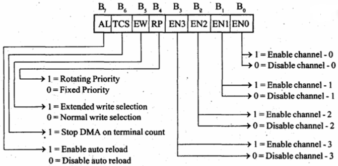
Operating Modes
The operating modes of 8237 are as follows:
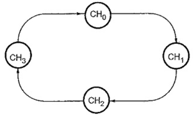
- Rotating priority mode
- Here, the priority of channels has a circular sequence.
- The channel that is serviced has the lowest priority and the channel present next to it has the highest priority.
- This is explained with the help of figure.
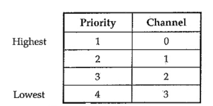
- Fixed priority mode
- Here, channel 0 has highest priority and channel 3 has the lowest priority.
- After one channel is recognized for service, other channels are prevented from interfering until the service is completed.
- Extended write mode
- It is used to provide alternate timing for the I/O or memory to write signals.
- This allows the devices to an early READY signal and prevents the unnecessary occurrence of wait states.
- It is done by activating MEMW and IOW signals.
- TC stop mode
- If TC is set, channel is disabled.
- Hence, it prevents further DMA operation on that channel.
- To enable DMA operation, it is necessary to set the enable bit of the channel present in the mode set register.
- If TC stop bit is not set then the presence of TC output has no effect on the channel enable bits.
- Auto load mode
- When turned ON, it enables block chaining operations.
- In this, channel 2 parameters are initialized for the first data block.
- They are automatically copied to channel 3 registers.
- When an update cycle is initialized, the channel 3 parameters are transferred to channel 2.
- This is auto reloaded and is used for applications like CRT refreshing.
Q8) Explain PPI pin diagram?
A8)
Pin Configuration
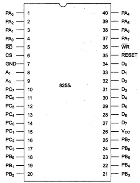
Pin Configuration of 8255
- It is also known as Programmable Peripheral Interface.
- It is a multi-port device.
- It has 24 I/O pins. They are divided into three 8-bit ports PA, PB, PC.
- Port A and port B are used as 8-bit I/O ports.
- Port C is used as an 8-bit I/O port or as two 4-bit I/O ports or produces handshake signals for ports A and B.
- CS: The chip selects CS (pin 6) is used to enable the 8255 chip. It is an active-low signal, hence is enabled when CS = 0.
- RESET: It is an input pin 35 and is connected to the RESET line of system 8085. When the system is reset, all the ports behave as input lines. This is done to prevent 8255 from being destroyed due to mismatch of ports.
- Eight data lines (D0–D7) are available to read/write data into the ports or control register under the status of the RD (pin 5) and WR (pin 36), which are active-low signals for read and write operations respectively.
- Address lines A1 and A0 allow to access a data register for each port or a control register, as listed below:
A1 | A0 | PORT SELECTED |
0 | 0 | PORT A |
0 | 1 | PORT B |
1 | 0 | PORT C |
1 | 1 | Control Register |
Operating Modes
There are two basic operating modes of 8255.
- Bit set/reset mode (BSR mode)
- Input/ output mode (I/O mode)
The modes selected by the D7 bit of the control word register are:
When D7 = 1, 8255 operates in I/O mode else BSR mode.
BSR MODE
The Bit Set/Reset (BSR) mode is available on port C only. Each and every line of port C (PC7 - PC0) can be set or reset by providing a suitable value to the control word register. BSR mode is independent and its selection does not affect the operation of other ports in I/O mode.

- D7 bit is always 0 for this mode.
- Bits D6, D5 and D4 are don't care bits.
- Bits D3, D2 and D1 are used for pin selection of Port C.
- Bit D0 is used to set/reset the above selected pin.
Selection of port C pin is determined as follows:
D3 | D2 | D1 | Bit/pin of port C selected |
0 | 0 | 0 | PC0 |
0 | 0 | 1 | PC1 |
0 | 1 | 0 | PC2 |
0 | 1 | 1 | PC3 |
1 | 0 | 0 | PC4 |
1 | 0 | 1 | PC5 |
1 | 1 | 0 | PC6 |
1 | 1 | 1 | PC7 |
For example:
If PC4 be set, then in the control word is,
- Since it is a BSR mode, D7 = '0'.
- Since D4, D5, D6 are don’t care hence assuming them to be '0'.
- PC4 has to be selected, hence, D3 = '1', D2 = '0', D1 = '0'.
- PC4 has to be set, hence, D0 = '1'.
Thus, as per the above values, 0AH (in hex) will be loaded into the Control Word Register (CWR).
I/O MODE
When D7 bit of the Control Word Register is 1, this mode is selected.
There are three I/O modes and they are:
- Mode 0 - Simple I/O
- Mode 1 - Strobed I/O
- Mode 2 - Strobed Bi-directional I/O
- Mode 0 – Simple or basic I/O mode:
Port A, B and C can work either as input or as output function. The outputs are latched but the inputs are not latched. It can handle interrupts.
- Mode 1 – Handshake or strobbed I/O: Here, either port A or B can work and port C is used to provide handshake signals. The outputs as well as inputs are latched. It can handle interrupts. Before actual data is transmitted, there is transmission of signal to match speed of CPU and printer.
- Mode 2 – Bidirectional I/O: In this mode only port A will work, port B can either is in mode 0 or 1 and port C bits are used as handshake signal. The outputs as well as inputs are latched. It has interrupt handling capability.
Q9) Explain the functional diagram of PPI?
A9)
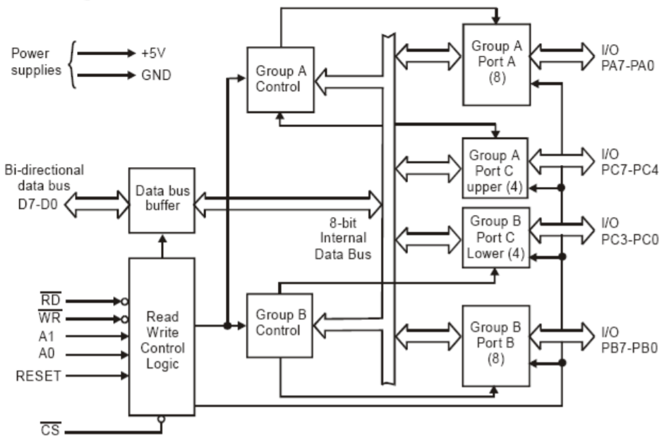
Fig. Functional Block Diagram
Control Word for I/O mode
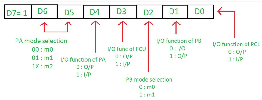
- The most significant bit (D7) is 1 for the I/O mode.
- D6 & D5: It is used to set the port A mode.
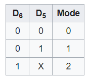
- D4: It is used to check whether port A is taking input or displaying the output. If it is 1 then input else output.
- D3: It is used to check whether port C higher bites takes input or output. If 1, then input else output.
- D2: It tells the mode of port B. If 0, then port B is in M0 mode else in M1 mode.
- D1: It is used to check whether port B is taking input or displaying output. If 1, then input else output.
- D0: It is used to tell whether port C lower bits is taking input or displaying output. If 1, then it takes input else displays output.
Q10) Explain 8253 PPI pin diagram?
A10)
Pin Configuration
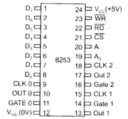
Fig. Pin Configuration of 8253
- It is a programmable counter / timer chip which is used as an Intel microcomputer peripheral.
- It uses nMOS technology with +5V supply and is packaged in a 24-pin plastic DIP.
- It is used as an event counter, elapsed time indicator, programmable one-shot etc.
- There are three counters, a data bus buffer, Read/Write control logic, and a control register. Each counter has two input signals - CLOCK & GATE, and one output signal - OUT.
Data Bus Buffer
It is a tri-state, bi-directional, 8-bit buffer, which is used to interface the 8253 to the system data bus. It has three basic functions −
- Programming the modes of 8253.
- Loading the count registers.
- Reading the count values.
Read/Write Logic
It includes 5 signals, i.e., RD, WR, CS, and the address lines A0 & A1. In the peripheral I/O mode, the RD and WR signals are connected to IOR and IOW and in the memory mapped I/O mode to MEMR and MEMW.
Address lines A0 & A1 of the CPU are connected to lines A0 and A1 of the 8253 and CS is tied to a decoded address.
A1 | A0 | Result |
0 | 0 | Counter 0 |
0 | 1 | Counter 1 |
1 | 0 | Counter 2 |
1 | 1 | Control Word Register |
X | X | No Selection |
Q11) Explain 8253 functional diagram?
A11)
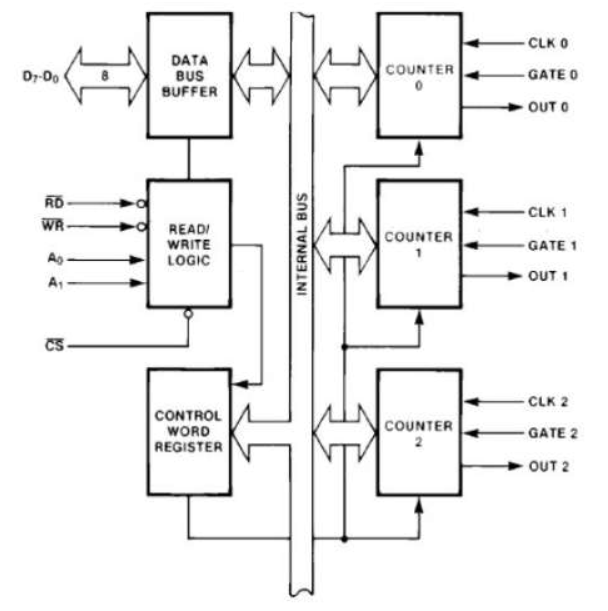
Figure. Block Diagram of 8253
Control Word Register
This register can be accessed when lines A0 & A1 are at logic 1.
It is used to write a command word, its mode and either a read or write operation.
Following table provides the result for various control inputs:
A1 | A0 | RD | WR | CS | Result |
0 | 0 | 1 | 0 | 0 | Write Counter 0 |
0 | 1 | 1 | 0 | 0 | Write Counter 1 |
1 | 0 | 1 | 0 | 0 | Write Counter 2 |
1 | 1 | 1 | 0 | 0 | Write Control Word |
0 | 0 | 0 | 1 | 0 | Read Counter 0 |
0 | 1 | 0 | 1 | 0 | Read Counter 1 |
1 | 0 | 0 | 1 | 0 | Read Counter 2 |
1 | 1 | 0 | 1 | 0 | No operation |
X | X | 1 | 1 | 0 | No operation |
X | X | X | X | 1 | No operation |
Operating Modes
8253 can be operated in 6 different modes. They are:
Mode 0 ─ Interrupt on Terminal Count
- It is used for generating an interrupt to the microprocessor after a certain interval.
- The output is low after the mode is set and remains LOW after the count value is loaded into the counter.
- The counter decrement continues till the terminal count is reached.
- The GATE signal remains high for normal counting. When it is low, counting is terminated and the current count is latched till it goes high again.
Mode 1 – Programmable One Shot
- It is used as a mono stable multi-vibrator.
- GATE is used as a trigger input in this mode.
- As the count is loaded the output remains high and a trigger is applied.
Mode 2 – Rate Generator
- The output is high after initialization.
- Whenever the count becomes zero, a low pulse is generated at the output and the counter is reloaded.
Mode 3 – Square Wave Generator
- This mode is same as Mode 2 except that the output remains low for half of the timer period and high for the next half of the period.
Mode 4 − Software Triggered Mode
- In this, the output remains high till the timer counts to zero and at this point the output is low and then goes high again.
- The count is latched when GATE LOW.
- As per the terminal count, for one clock cycle the output goes low then goes HIGH. The low pulse is used as a strobe.
Mode 5 – Hardware Triggered Mode
- This mode generates a strobe as a result to an externally generated signal.
- It is same as mode 4 except that the counting is initiated by a signal at the gate input.
- As soon as it is initialized, the output goes high.
- When the terminal count is reached, the output goes low for one clock cycle.
Q12) Explain 8259 programmable interrupt controller?
A12)
It is commonly known as PIC (Programmable Interrupt controller).
Block Diagram
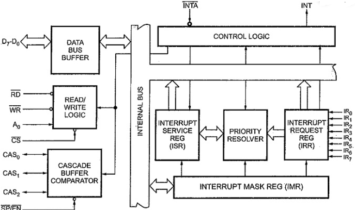
Fig. Block Diagram of 8259
Data Bus Buffer:
The data bus buffer allows the 8086 to send control words to the 8259A. The 8-bit data bus buffer also allows the 8259A to send interrupt opcode and address of the interrupt service subroutine to the 8086.
Read/Write Logic:
The RD and WR inputs control the data flow on the data bus when the device is selected by asserting its chip select (CS) input low.
Control Logic:
This block has an input and an output line. If the 8259A is properly enabled, the interrupt request will cause the 8259A to assert its INT output pin high.
Interrupt Request Register (IRR):
It is used to store all the interrupt levels which are requesting the service. The eight interrupt inputs set corresponding bits of the Interrupt Request Register upon service request.
Interrupt Service Register (ISR):
It stores all the levels that are currently being serviced.
Interrupt Mask Register (IMR):
It stores the masking bits of the interrupt lines to be masked. This register can be programmed by an Operation Command Word (OCW).
Priority Resolver:
It determines the priorities of the bits set in the IRR. The bit corresponding to the highest priority interrupt input is set in the ISR during the INTA input.
Cascade Buffer Comparator:
It generates control signals necessary for cascade operations. It also generates Buffer-Enable signals. Here, the former is called a master, and the latter are called slaves. The 8259 can be set up as a master or a slave by the SP/EN pin.
CAS0— CAS2
For a master 8259, the CAS0-CAS2 pins are output pins, and for slave 8259, these are input pins. When the 8259 is a master (that is, when it accepts interrupt requests from other 8259s), the CALL opcode is generated by the Master in response to the first INTA.
SP / EN (Slave Program /Enable Buffer):
The SP/EN signal is tied high for the master. However, it is grounded for the slave.
Priority Modes and Other Features:
The various modes of operation of the Block Diagram of 8259 Programmable Interrupt Controller are:
o Fully Nested Mode,
o Special Fully Nested Mode (SFNM)
o Rotating Priority Mode,
o Special Masked Mode, and
o Polled Mode.
Fully Nested Mode (FNM):
After initialization, the 8259A operates in fully nested mode so it is called default mode. In this mode, IR0 has highest priority and IR7 has lowest priority. When the interrupt is acknowledged, it sets the corresponding bit in ISR. This bit will inhibit all interrupts of the same or lower level, however it will accept higher priority interrupt requests. The vector address corresponding to this interrupt is then sent. The bit in the ISR will remain set until an EOI command is issued.
End of Interrupt (EOI):
- The ISR bit is reset by an EOI command issued by the CPU, usually just before exiting from the interrupt routine.
- In the Fully Nested Mode, the highest level in the ISR would necessarily correspond to the last interrupt acknowledged and serviced. In such a case, a non-specific EOI command may be issued by the CPU.
Special Fully Nested Mode (SFNM):
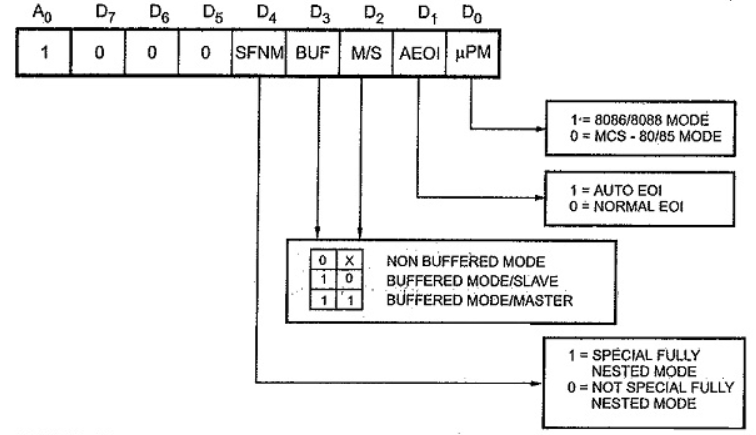
The Special Fully Nested Mode (SFNM) is used to avoid this problem. The SFNM is set up by ICW4 during initialization. It is similar to the FNM.
Rotating Priority Mode:
The Rotating Priority mode can be set in Automatic Rotation, and Specific Rotation.
Automatic Rotation:
In this mode, a device, after being serviced, receives the lowest priority. The device just been serviced, will receive the seventh priority. Here IR3 has just been serviced.

Specific Rotation:
In this, the lowest priority can be assigned to any interrupt input (IR0 to IR7) thus fixes all other priorities.
For example, if the lowest priority is assigned to IR2, other priorities are as shown below.

Special Mask Mode:
If any interrupt is in service, then the corresponding bit is set in ISR and the lower priority interrupts are inhibited. Some applications may require an interrupt service routine to dynamically alter the system priority structure during its execution under software control.
Poll Mode:
In this mode the INT output is not used. The microprocessor checks the status of interrupt requests by issuing poll command. The microprocessor reads contents of 8259A after issuing poll command. During this read operation the 8259A provides polled word and sets ISR bit of highest priority active interrupt request FORMAT.

I = 1 —> One or more interrupt requests activated.
I = 0 —> No interrupt request activated.
W2 W1 W0 —>Binary code of highest priority active interrupt request.
Control word (ICW1):
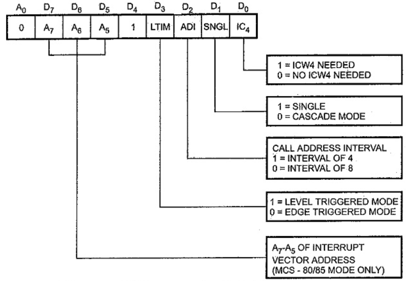
A write command issued to the 8259 with A0 = 0 and D4 = 1 is interpreted as ICW1, which starts the initialization sequence. It specifies,
- Single or multiple 8259As in the system
- 4- or 8-bit interval between the interrupt vector locations.
- The address bits A7 – A5 of the CALL instruction. (3 bits of lower byte address of CALL is given by user, rest bits are inserted by 8259A)
- Edge triggered or level triggered interrupts.
- ICW4 is needed or not.
Control word (ICW2):

A write command following ICW1, with A0 = 1 is interpreted as ICW2. This is used to load the high order byte of the interrupt vector address of all the interrupts.
Control word (ICW3):
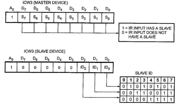
Control word (ICW4):
Q13) Explain 8251 USART?
A13)
8251 universal synchronous asynchronous receiver transmitter (USART) acts as a mediator between microprocessor and peripheral to transmit serial data into parallel form and vice versa.
- It takes data serially from peripheral (outside devices) and converts into parallel data.
- After converting the data into parallel form, it transmits it to the CPU.
- Similarly, it receives parallel data from microprocessor and converts it into serial form.
- After converting data into serial form, it transmits it to outside device (peripheral).
Pin Configuration
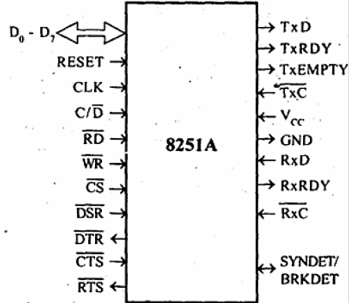
Fig. Pin Configuration
Data Bus: Bi-directional, tri-state, 8-bit Data Bus. This pin allows transfer of bytes between the CPU and the 8251A.
RD (Read): A low on this input allows the CPU to read data or status bytes from 8251A
WR (Write): A low on this input allows the CPU to write data or command word to the 8251A.
CLK (Clock): The CLK input is used to generate internal device timing. The frequency of CLK must be greater than 30 times the receiver or transmitter data bit rates.
RESET: A high on this input forces the 8251A into an “Idle” mode. The device will remain at “Idle” until a new set of control words is written into the 8251 Pin Diagram to program its functional definition.
C/D (Control /Data): This input in conjunction with the WR and RD inputs, informs the 8251A that the word on the Data Bus is either a data character control word or status information as shown in table.
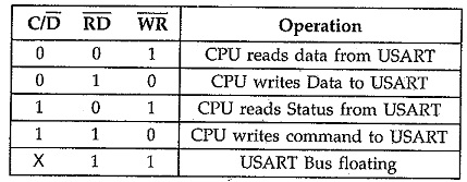
CS (Chip Select): A low on this input allows communication between CPU and 8251A
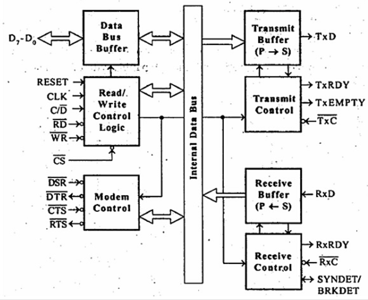
Fig. Block Diagram
It contains the following blocks:
- Data bus buffer – This block helps in interfacing the internal data bus of 8251 to the system data bus. The data transmission is possible between 8251 and CPU by the data bus buffer block.
- Read/Write control logic – It is a control block for overall device. It controls the overall working by selecting the operation to be done. The operation selection depends upon input signals as:
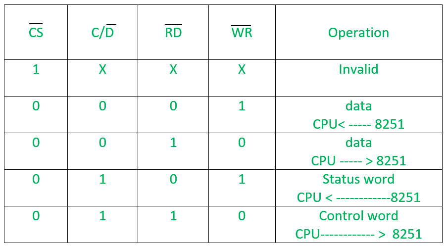
In this way, this unit selects one of the three registers- data buffer register, control register, status register.
- Modem control (modulator/demodulator) –
A device converts analog signals to digital signals and vice-versa and helps the computers to communicate over telephone lines or cable wires. The following are active-low pins of Modem.- DSR: Data Set Ready signal is an input signal.
- DTR: Data terminal Ready is an output signal.
- CTS: It is an input signal which controls the data transmit circuit.
RTS: It is an output signal which is used to set the status RTS.
- Transmit buffer –
This block is used for parallel to serial converter that receives a parallel byte for conversion into serial signal and further transmission onto the common channel.- TXD: It is an output signal, if its value is one, means transmitter will transmit the data.
- Transmit control –
This block is used to control the data transmission with the help of following pins:- TXRDY: It means transmitter is ready to transmit data character.
- TXEMPTY: An output signal which indicates that TXEMPTY pin has transmitted all the data characters and transmitter is empty now.
- TXC: An active-low input pin which controls the data transmission rate of transmitted data.
- Receive buffer –
This block acts as a buffer for the received data.- RXD: An input signal which receives the data.
- Receive control –
This block controls the receiving data.- RXRDY: An input signal indicates that it is ready to receive the data.
- RXC: An active-low input signal which controls the data transmission rate of received data.
- SYNDET/BD: An input or output terminal. External synchronous mode-input terminal and asynchronous mode-output terminal.
Q14) Explain RS-232?
A14)
RS232 is an Interface and the protocol between DTE (data terminal equipment) and DCE (data communication equipment) using serial binary data exchange. Here C is used for the current version. Universal Asynchronous Data Receiver & Transmitter (UART), attached in a motherboard, used in connection with RS232 for transmitting data to any serial device like modem or printer from its DTE interface.
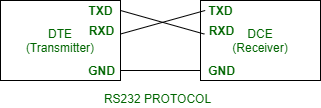
Fig. RS232 Protocol
Electrical Specifications:
Voltages:
There can be two states in the signal level of RS232C pins.
- Mark state – It is the high bit which is represented by binary 1 and have negative voltages. Its voltage limits for transmitting signal ranges from -5 to -15V. Its voltage limits for receiving signals ranges from -3 to -25V.
- Space state – It is the low bit which is represented by binary 0 and have positive voltages. Its voltage limits for transmitting signal ranges from +5 to +15V. Its voltage limits for receiving signals ranges from +3 to +25V.
Cables and Wires: The maximum cable length for RS232C is equals to 15.24 metres or equal to the capacitance of 2500pF. Limits for impedance of wires ranges from 3 ohms to 7 ohms.
Data and Slew rates: Rate of data transmission through RS232C is up to 20Kbps. The rate of change in signal levels i.e., slew rate is up to 30V/microsecond.
Current:
Maximum current rating is 3Amps at the maximum operating voltage of 250V AC.
Pins and Working:
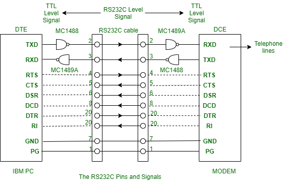
Fig .RS232 Pin and Signal
RS232C requires 25 pins connector for connecting DTE and DCE. Here is the list of pins and signals of RS232C and the connection between DTE and DCE using drivers and receivers.
- TXD & RXD – Transmit Data and Receive Data on the DTE are the serial data lines. These lines have opposite functions on a DCE. TXT sends outgoing data to DCE. RXD receives incoming data from DTE.
- RTS & CTS – Transmitter activates the Request to Send when it requires to transmit data over the line. The line itself gets deactivated when the communication stops. Receiver activates the Clear to Send to tell the transmitter whether it is ready or not to receive the data. It remains active during the transmission.
- DTR & DSR – Through the Data Terminal Ready line, DTE informs the DCE that it is in online mode and the process of communication can occur. The main task of Data Set Ready signal is to inform that DCE is ready for communication.
- DCD – DCE activates the Data Carrier Detect in order to show that it has been connected to DTE.
- RI – When an incoming call on the telephone line is detected by DCE, then the Ring Indicator gets activates.
Handshaking:
Before the actual data transfer, signals are transmitted from DTE to DCE in order to make connections by a process known as handshaking. Following is the sequence of signal handshaking:
- Initially, the computer activates RTS signal to modem when a data is transferred from computer to modem.
- Modem in turn activates the DCD and then the CTS gets activated.
- Computer then sends data on TXD. After the data transmission is completed, the computer deactivates the RTS which causes the modem to deactivate CTS.