Unit – 5
Assembly programming and instruction of 8051 and Interfacing
Q1) Explain 8051 assembly programming?
A1)
Each line or statement of the assembly language program of 8051 Microcontroller consists of three fields: Label, Instruction and Comments.

Label
The Label is programmer chosen name for a Memory Location or a statement in a program. The Label part of the statement is optional and if present, the Label must be terminated with a Colon (:).
Instruction
The Instruction is the main part of the 8051 Microcontroller Assembly Language Programming as it is responsible for the task performed by the Microcontroller.
Comment
Comments are statements included by the developer for easier understanding of the code and is used for proper documentation of the Program
Q2) Explain assembly and running in 8051?
A2)
The steps to create an executable Assembly language program are outlined as follows.
- First, we use an editor to type in a program. Many editors or word processors are available that can be used to create and/or edit the program. The most widely used editor is MS-DOS EDIT program or Notepad in Windows which comes with all Microsoft operating systems.
Note: the editor must be able to produce an ASCII file. For many assemblers, the file names follow the usual DOS conventions, but the source file has the extension “asm” or “src”, depending on which assembler you are using.
- The “asm” source file containing the program code created in step 1 is fed to an 8051 assembler. The assembler converts the instructions into machine code. The assembler will produce an object file and list file. The extension for object file is “obj” while the extension for list file is “1st”.
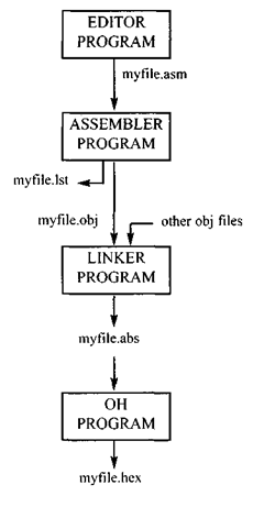
Figure. Steps to create a program
2. Assemblers require a third step called linking. The link program takes one or
more object files and produces an absolute object file with the extension “abs”
3. Next, the “abs” file is fed into a program called “OH” object to hex convert
er which creates a file with extension “hex” that is ready to burn into ROM.
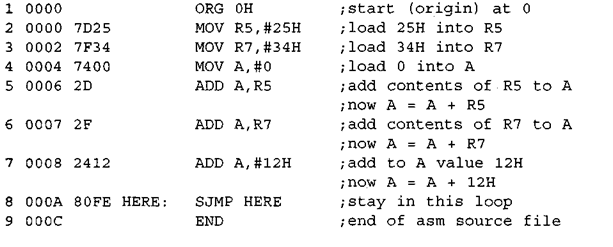
Q3) Explain the data types?
A3)
DB (define byte)
- It is used to define the 8-bit data.
- When DB is used to define data, the numbers can be in decimal, binary, hex, or ASCII formats.
- “B” (binary) and “H” (hexadecimal) is required.
- To indicate ASCII, simply place the characters in quotation marks
- The DB directive is the only directive that can be used to define ASCII strings larger than two characters; therefore, it should be used for all ASCII data definitions.
Following are some DB examples:
ORG 2000H
DATA1: DB 28; DECIMAL NUMBER 28
DATA2: DB 1234h; HEXADECIMAL
DATA3: DB "ABCD"; ASCII CHARACTER
Q4) Explain the assembler directives?
A4)
ORG (origin)
- The ORG directive is used to indicate the beginning of the address.
- The number that comes after ORG can be either in hex or in decimal.
- If the number is not followed by H, it is decimal and the assembler will convert it to hex.
EQU (equate)
- This is used to define a constant without occupying a memory location.
- The following uses EQU for the counter constant and then the constant is used to load the R3 register.
CONST EQU 25H
MOV A, #CONST; COPY 25 INTO A
END
- This indicates to the assembler the end of the source (asm) file.
- The END directive is the last line of an 8051 program, meaning that in the source code anything after the END directive is ignored by the assembler.
Q5) Explain the arithmetic instructions?
A5)
Using Arithmetic Instructions, one can perform addition, subtraction, multiplication and division. It consists of increment by one, decrement by one and a special instruction called Decimal Adjust Accumulator.
The Mnemonics associated with the Arithmetic Instructions of the 8051 Microcontroller Instruction Set are:
The arithmetic instructions have no knowledge about the data format that is signed, unsigned, ASCII, BCD, and so on. The operations performed by the arithmetic instructions affect flags like carry, overflow, zero, etc. in PSW Register.
Mnemonic | Instruction | Description | Addressing Mode |
ADD | A, #data | A <- A + Data | Immediate |
A, Rn | A<- A + Rn | Register | |
A, Direct | A<- A + (Direct) | Direct | |
A, @Ri | A<- A + @Ri | Indirect | |
ADDC | A, #data | A <- A + Data + C | Immediate |
A, Rn | A<- A + Rn + C | Register | |
A, Direct | A<- A + (Direct)+C | Direct | |
A, @Ri | A<- A + @Ri +C | Indirect | |
SUBB | A, #data | A <- A – Data | Immediate |
A, Rn | A<- A- Rn | Register | |
A, Direct | A<- A - (Direct) | Direct | |
A, @Ri | A<- A XRL-Ri | Indirect | |
MUL AB | Multiply A with B | ||
DIV AB | Divide A by B | ||
DEC A | A, #data | A <- A -1 | |
A, Rn | Rn <-Rn -1 | ||
A, Direct | (Direct) <- (Direct) -1 | ||
A, @Ri | @Ri<- @Ri -1 | ||
INC A | A, #data | A <- A+1 | |
A, Rn | Rn <-Rn +1 | ||
A, Direct | (Direct)<- (Direct) +1 | ||
A, @Ri | @Ri<- @Ri+1 | ||
DAA | A | Decimal Adjust Accumulator |
Q6) Explain logical instructions?
A6)
Logical Instructions perform logical operations like AND, OR, XOR, NOT, Rotate, Clear and Swap. Logical Instruction are performed on bytes of data on a bit-by-bit basis.
Mnemonics associated with Logical Instructions are as follows:
Mnemonic | Instruction | Description | Addressing Mode |
ANL | A, #data | A <- A AND Data | Immediate |
A, Rn | A<- A AND Rn | Register | |
A, Direct | A<- A AND (Direct) | Direct | |
A, @Ri | A<- A AND @Ri | Indirect | |
Direct A | (Direct) <- (Direct) AND A | Direct | |
Direct, # Data | (Direct) <- (Direct) AND # Data | Direct | |
ORL | A, #data | A <- A OR Data | Immediate |
A, Rn | A<- A OR Rn | Register | |
A, Direct | A<- A OR (Direct) | Direct | |
A, @Ri | A<- A OR @Ri | Indirect | |
Direct A | (Direct) <- (Direct) OR A | Direct | |
Direct, # Data | (Direct) <- (Direct) OR # Data | Direct | |
XRL | A, #data | A <- A XRL Data | Immediate |
A, Rn | A<- A XRL Rn | Register | |
A, Direct | A<- A XRL (Direct) | Direct | |
A, @Ri | A<- A XRL @Ri | Indirect | |
Direct A | (Direct) <- (Direct) XRL A | Direct | |
Direct, # Data | (Direct) <- (Direct) XRL # Data | Direct | |
CLR | A | A<-00H | |
CPL | A | A<-A | |
RL | A | Rotate ACC Left | |
RLC | A | Rotate ACC Left through carry | |
RR | A | Rotate ACC right | |
RRC | A | Rotate ACC right through carry | |
SWAP | A | Swap nibbles within ACC |
Q7) Explain the program for logical operations?
A7)
Org 8000h
Mov r0, #0fh
Mov r1, #foh
Mov r2, #66h
; And operation
Mov a, #ffh
Anl a, r0
Mov r3, a
; Or operation
Mov a, #ffh
Orl a, r1
Mov r4, a
; Xor operation
Mov a, 03h
Mov a, #ffh
Xrl a, r2
Mov r5, a
Lcall 0003h
End
Org 9000h
; clear register A
Mov a, #0fh
Clr a
Mov r0, a
; swap nibbles of register A
Mov a, #56h
Swap a
Mov r1, a
; Complement the bit of register A
Mov a, #66h
Cpl a
Mov r2, a
; Rotate the register contents towards right
Mov a, #63h
Rr a
Xrl a, r
Mov r3, a
; Rotate the register contents towards left
Mov a, #43h
Rl a
Xrl a, r
Mov r4, a
Lcall 0003h
End
Q8) Explain jump call and loop instructions?
A8)
JZ label; Jump if A=0
JNZ label; Jump if A! =0
DJNZ reg, label; Decrement and Jump if A (or reg.)! =0
CJNE A, byte; Compare and Jump if A! =byte
CJNE reg, #data; Compare and Jump if byte! =data
JC; Jump if Carry=1 J
NC; Jump if Carry=0
JB; Jump if bit =1
JNB; Jump if bit =0
JBC; Jump if bit=1 and clear bit
LCALL: 3-byte instruction • When subroutine is called – Control is transferred to that subroutine – Processor saves the PC onto the Stack and begins to fetch instructions from new location. – RET (return to caller) POP from Stack to PC.
ACALL:
2-byte instruction
ACALL’s target address must be with in a 2KB range
Write a program to clear Accumulator [A], then Add 5 to the accumulator 20 times:
Answer:
This program adds value 3 to the Accumulator 20 times
MOV A, #0; Accumulator=0, Clear Accumulator
MOV R2, #20; Load counter R2=20
AGAIN: ADD A, #05; Add 05 to Accumulator
DJNZ R2, AGAIN; Repeat Until R2=0 [20 times]
MOV R5, A; Save Accumulator in R5
Q9) Explain I/O port programming?
A9)
There are four ports in 8051 microcontroller named as P0, P1, P2 and P3. Each port has 8 pins. For Port 0 8 pins names as P0.0, P0.1, P0.2, P0.3, P0.4, P0.5, P0.6, and P0.7. All the ports upon RESET are ready to be configured or used as output. To use all these ports as an input port, it must be programmed.
PORT 0:
Port 0 has 8 pins P0.0, P0.1, P0.2, P0.3, P0.4, P0.5, P0.6, and P0.7, pins 39, 38, 37, 36, 35, 34, 33, 32. This port can be used for input or output. Each pin of the port 0 must be connected externally to a 10K Ohm pull-up resistor, to use Port 0 as both input or output ports. This is because the Port 0 [P0] is an open drain. This is not the case in other ports P1, P2 and P3. 'Open drain' is a term used for MOS chips, as 'open collector' is used for TTL chips. To use Port 0 for both input and output, have to connect Port 0 to pull-up resistors. When external pull-up resistors connected upon reset, Port 0 is configuring as output port.
Role of Port 0 as Input Port:
To make Port 0 as input port, the pull up resistors are connected to port 0. The port must be programmed by writing 1 to all the bits. Let’s examine the code example below in which the Port 0 is configured first as an input port by writing 1's to it and then data is received from that port and send to Port 1 [P1].
MOV A, #0FFH; Load accumulator with value FFH in hex or 255 in decimal
MOV P0, A; Make Port 0 as an input port by writing all 1's to it
BACK: MOV A, P0; Get data from Port 0
MOV P1, A; Send it to Port 1
SJMP BACK; Keep doing it repeatedly
The Dual Role of Port 0:
Port 0 can be used to configures for both data and address. The Port 0 is also designated as AD0 - AD7. When connecting an 8051 to an external memory, port 0 provides both address and data. The 8051 multiplexes address and data through Port 0 to save pins. Address latch enable [ALE] indicates if Port 0 has address or data. When ALE=0, it provides data D0 - D7, but when ALE = 1, it has address A0 - A7. With the help of 74LS373 latch, ALE is used for demultiplexing address and data.
PORT 1:
Port 1 has a total of 8 pins. P1.0, P1.1, P1.2, P.13, P1.4, P1.5, P1.6, and P1.7. Port 1 can be used as an input or output. As compares to Port 0, this port does not need any pull-up resistors. Port 1 already has internally connected pull-up resistors. Port 1 is configured as an output port when reset.
Example # 1:
Let’s examine the code, which will continuously send Output to Port 1 the alternating values 55H and AAH
MOV A, #55H
BACK MOV P1, A
ACALL DELAY
CPL A
SJMP BACK
The Role of Port 1 as Input Port:
The Port 1 must be programmed by writing 1's to all the bits in order to make Port 1 as an input port.
Example # 2:
MOV A, #0FFH; Load Accumulator with FFH in hex
MOV P1, A; Make P1 an input Port, by writing all 1's to Port 1
MOV A, P1; Get data from Port 1
MOV R3, A; Save data in register R3
ACALL DELAY; Wait
MOV A, P1; Get another data from Port 1
MOV R4, A; Save data in register R4
ACALL DELAY; Wait
MOV A, P1; Get another data from Port 1
MOV R5, A; Save data in register R5
In Example # 2 above, the Port 1 is configuring as input port by writing 1's to it, then data is received from that port and saved in R3, R4 and R5.
PORT 2:
Port 2 also has total of 8 pins. P2.0, P2.1, P2.2, P2.3, P2.4, P2.5, P2.6, and P2.7. Port 2 can be used for input or output port. To make Port 2 as an input, the Port 2 must be programmed by writing 1's to all bits.
Example # 3:
MOV A, #55H
BACK: MOV P2, A
ACALL DELAY
CPL A
SJMP BACK
In Example # 3 above, the code will send out continuously to Port 2 an alternating values 55H and AAH to toggle the bits or Port 2 continuously.
The Role of Port 2 as an Input Port:
The Port 2 must be programmed by writing 1's to all the port 2 bits to make Port 2 as an input port.
Example #4:
MOV A, #0FFH; Load accumulator with value 0FFH in hex
MOV P2, A; Make Port 2 an input port by writing 1's to all bits of port 2
BACK: MOV A, P2; Get data from Port 2
MOV P1, A; Send data to Port 1
SJMP BACK; Keep doing it repeatedly
In Example # 4 above, the Port 2 is configuring as input port by writing all 1's, then data is received from that port and is sent to Port 1 continuously.
The Dual Role or Port 2:
Port 2 has dual role. Port 2 is also designated as A8 - A15. This indicates that Port 2 has a dual function. An 8031 microcontroller is capable of accessing 64K bytes of external memory, it needs a path for the 16 bits of the address. P0 provides the lower 8 bits via A0 - A7 while Port 2 provides bits A8 - A15 of the address. When the 8031 is connected to external memory, Port 2 is used for the upper 8 bits of the 16-bit address, and it cannot be used for input / output operations.
Port 3:
Port 3 has total 8 Pins. P3.0, P3.1, P3.2, P3.3, P3.4, P3.5, P3.6, and P3.7. Pins 10, 11, 12, 13, 14, 15, 16, and 17. Port 3 can be sued as an input port or output port. Port 3 does need any pull-up resisters, just like the Port 1 and Port 2 does not require pull-up resistors. Only Port 0 require Pull-up resistors. Port 3 configured as an output port upon system reset. Port 3 has additional function of providing signals of interrupts.
Alternate Functions of Port 3:
PORT 3 BIT FUNCTION PIN
P3.0 RxD [Receive Serial Communications Signals] 10
P3.1 TxD [Transmit Serial Communications Signals] 11
P3.2 INT0 [External Interrupt 0] 12
P3.3 INT1 [External Interrupt 1] 13
P3.4 T0 [Timer 0] 14
P3.5 T1 [Timer 1] 15
P3.6 WR [Write Signals of External Memory] 16
P3.7 RD [Read Signals of External Memory] 17
Q10) Explain the programming of 8051 timers?
A10)
In order to program 8051 timers, it is important to know the calculation of initial count value to be stored in the timer register.
The calculations are as follows. In any mode,
Timer Clock period = 1/Timer Clock Frequency. = 1/ (Master Clock Frequency/12)
- Mode 1 (16-bit timer/counter) Value to be loaded in decimal = 65536 – (Delay Required/Timer clock period). Convert the answer into hexadecimal and load onto THx and TLx register. (65536D = FFFFH+1).
b. Mode 0 (13-bit timer/counter) Value to be loaded in decimal = 8192 – (Delay Required/Timer clock period) Convert the answer into hexadecimal and load onto THx and TLx register. (8192D = 1FFFH+1)
c. Mode 2 (8 bit auto reload) Value to be loaded in decimal = 256 – (Delay Required/Timer clock period) Convert the answer into hexadecimal and load onto THx register.
Upon starting the timer this value from THx will be reloaded to TLx register. (256D = FFH+1)
Steps for programming timers in 8051
Mode 1:
Load the TMOD value register indicating which timer (0 or 1) is to be used and which timer mode is selected. Load registers TL and TH with initial count values.
- Start the timer by the instruction “SETB TR0” for timer 0 and “SETB TR1” for timer 1.
- Keep monitoring the timer flag (TF) with the “JNB TFx, target” instruction to see if it is raised. Get out of the loop when TF becomes high.
- Stop the timer with the instructions “CLR TR0” or “CLR TR1”, for timer 0 and timer 1, respectively.
- Clear the TF flag for the next round with the instruction “CLR TF0” or “CLR TF1”, for timer 0 and timer 1, respectively.
- Go back to step 2 to load TH and TL again.
Mode 0:
The programming techniques mentioned here are also applicable to counter/timer mode 0. The only difference is in the number of bits of the initialization value.
Mode 2:
- Load the TMOD value register indicating which timer (0 or 1) is to be used; select timer mode
- Load TH register with the initial count value. As it is an 8-bit timer, the valid range is from 00 to FFH.
- Start the timer. Keep monitoring the timer flag (TFx) with the “JNB TFx, target” instruction to see if it is raised.
- Get out of the loop when TFx goes high. Clear the TFx flag.
- Go back to step 4, since mode 2 is auto-reload.
Q11) Write an 8051 C program to toggle only pin PI.5 continuously every 250 ms. Use Timer 0, mode 2 (8-bit auto-reload) to create the delay.
A11)
#include<reg51.h>
Void TOM2Delay(void);
Sbit mybit=P1^5;
Void main(void)
{
Unsigned char x,y;
While(1)
{
Unsigned char x,y;
While(1)
{
Mybit= ˜ mybit;
For(x=0;x<250;x++)
For(y=0;y<36;y++)
TOM2Delay();
}
}
256-23 = 233
23 x 1.085 us = 25 us
25 us x 250 x 40 = 250 ms by calculation.
However, the scope output does not give us this result. This is due to overhead of the for loop in C. To correct this problem, we put 36 instead of 40.
Q12) Write an 8051 C program to create a frequency of 2500 on pin P2.7. Use Timer 1 mode 2 to create delay.
A12)
# include<reg51.h>
Void T1M2Delay(void);
Sbit mybit= P2^7;
Void main(void)
{
Unsigned char x;
While(1)
{
Mybit= ˜ mybit;
T1M2Delay();
}
}
Void TIM2Delay(void)
TMOD = 0x20;
TH1=184;
TR1=1;
While(TF1==0);
TR1=0;
TF1=0;
}
1/2500 Hz = 400μs
400μs/2 = 200μs
200μs/1.085μs= 184
Q13) Explain serial port programming?
A13)
Since IBM PC/compatible computers are so widely used to communicate with 8051-based systems, serial communications of the 8051 with the COM port of the PC will be emphasized.
To allow data transfer between the PC and an 8051 system without any error, we must make sure that the baud rate of the 8051 system matches the baud rate of the PC‟s COM port.
Baud rate in the 8051
The 8051 transfers and receives data serially at many different baud rates. Serial communications of the 8051 is established with PC through the COM port. It must make sure that the baud rate of the 8051 system matches the baud rate of the PC's COM port/ any system to be interfaced. The baud rate in the 8051 is programmable. This is done with the help of Timer.
When used for serial port, the frequency of timer tick is determined by (XTAL/12)/32 and 1 bit is transmitted for each timer period. The Relationship between the crystal frequency and the baud rate in the 8051 is that the 8051 divides the crystal frequency by 12 to get the machine cycle frequency which is shown in figure.

Figure. Oscillatory Frequency
Here the oscillator is XTAL = 11.0592 MHz, the machine cycle frequency is 921.6 kHz. 8051's UART divides the machine cycle frequency of 921.6 kHz by 32 once more before it is used by Timer 1 to set the baud rate. 921.6 kHz divided by 32 gives 28,800 Hz. Timer 1 must be programmed in mode 2, that is 8-bit, auto-reload.
Calculation of baud rate:
In serial communication if data transferred with a baud rate of 9600 and XTAL used is 11.0592 then following is the steps followed to find the TH1 value to be loaded.
Clock frequency of timer clock: f = (11.0592 MHz / 12)/32 = 28,800Hz .
Time period of each clock tick: T0 = 1/f = 1/28800
Duration of timer: n*T0 (n is the number of clock ticks) 9600 baud ->duration of 1 symbol:
1/9600 1/9600 = n*T0 = n*1/28800 n = f/9600 = 28800/9600 = 3 ->TH1 =-3
Similarly, for baud 2400 n = f/2400 = 12 ->TH1 = -12
Example:
Set baud rate at 9600
MOV TMOD, #20H; timer 1, mode 2(auto reload)
MOV TH1, #-3; To set 9600 baud rate
SETB TR1; start timer 1
Q14) Write a Program to transfer letter “D” serially at 9800baud, continuously?
A14)
MOV TMOD, #20H; timer 1, mode 2(auto reload)
MOV TH1, #-3; 9600 baud rate
MOV SCON, #50H; 8-bit, 1 stop,
REN enabled
SETB TR1; start timer 1
AGAIN: MOV SBUF, #” D”; letter “D” to transfer
HERE: JNB TI, HERE; wait for the last bit
CLR TI; clear TI for next char
SJMP AGAIN; keep sending A
Q15) Write a Program to receive bytes of data serially, and put them in P2, set the baud rate at 9600, 8-bit data, and 1 stop bit:
A15)
MOV TMOD, #20H; timer 1, mode 2(auto reload)
MOV TH1, #-3; 9600 baud rate MOV SCON, #50H; 8-bit, 1 stop,
REN enabled SETB TR1; start timer 1
HERE: JNB RI, HERE; wait for char to come in
MOV A, SBUF; saving incoming byte in A
MOV P2, A; send to port 1
CLR RI; get ready to receive next byte
SJMP HERE; keep getting data
Q16) Explain interrupt programming?
A16)
Interrupt Structure of 8051 Microcontroller
After 'RESET' all the interrupts get disabled, and therefore, all the interrupts are enabled by software. From all the five interrupts, if anyone or all interrupt are activated, this will set the corresponding interrupt flags as represent in the figure which corresponds to Interrupt structure of 8051 microcontroller:
Interrupts in 8051 Microcontroller
All the interrupts can be set or cleared by some special function register that is also known as interrupt enabled (IE), and it is totally depends on the priority, which is executed by using interrupt priority register.
Interrupt Enable (IE) Register
IE register is used for enabling and disabling the interrupt. This is a bit addressable register in which EA value must be set to one for enabling interrupts. The individual bits in this register enables the particular interrupt like timer, serial and external inputs. Consider in the below IE register, bit corresponds to 1 activate the interrupt and 0 disable the interrupt.
Interrupt Priority Register (IP)
Using IP register, it is possible to change the priority levels of an interrupts by clearing or setting the individual bit in the Interrupt priority (IP) register as shown in figure. It allows the low priority interrupt can interrupt the high-priority interrupt, but it prohibits the interruption by using another low-priority interrupt. If the priorities of interrupt are not programmed, then microcontroller executes the instruction in a predefined manner and its order are INT0, TF0, INT1, TF1, and SI.
Interrupt programming in 8051
Timer Interrupt Programming: In microcontroller Timer 1 and Timer 0 interrupts are generated by time register bits TF0 AND TF1. This timer interrupts programming by C code involves:
Selecting the configuration of TMOD register and their mode of operation.
Enables the IE registers and corresponding timer bits in it.
Choose and load the initial values of TLx and THx by using appropriate mode of operation.
Set the timer run bit for starting the timer.
Write the subroutine for a timer and clears the value of TRx at the end of the subroutine.
Let's see the timer interrupt programming using Timer0 model for blinking LED using interrupt method:
#include< reg51 .h>
Sbit Blink Led = P2^0; // LED is connected to port 2 Zeroth pin
Void timer0_ISR (void) interrupt 1 //interrupt no. 1 for Timer0
{
Blink Led=~Blink Led; // Blink LED on interrupt
TH0=0xFC; // loading initial values to timer
TL0=0x66;
}
Void main()
{
TMOD=0x0l; // mode 1 of Timer0
TH0 = 0xFC: // initial value is loaded to timer
TL0 = 0x66:
ET0 =1; // enable timer 0 interrupt
TR0 = 1; // start timer
While (1); // do nothing
}
Q17) Explain hardware interrupt programming?
A17)
External Hardware Interrupt Programming
Microcontroller 8051 is consisting of two external hardware interrupts: INT0 and INT1 as discussed above. These interrupts are enabled at pin 3.2 and pin 3.3. It can be level triggered or edge triggered. In level triggering, low signal at pin 3.2 enables the interrupt, while at pin 3.2 high to low transition enables the edge triggered interrupt.
Enables the equivalent bit of external interrupt in Interrupt Enable (IE) register.
If it is level triggering, then write subroutine appropriate to this interrupt, or else enable the bit in TCON register corresponding to the edge triggered interrupt.
Consider the edge triggered external hardware interrupt programming is: -
Void main()
{
IT0 = 1; // Configure interrupt 0 for falling edge on INT0
EXO = 1; // Enabling the EX0 interrupt
EA =1; // Enabling the global interrupt flag
}
Void ISR_ex0(void) interrupt 0
{
<body of interrupt>
}
Q18) Explain serial communication interrupt programming?
A18)
It is used when there is a need to send or receive data. Since one interrupt bit is used for both Transfer Interrupt (TI) and Receiver Interrupt (RI) flags, Interrupt Service Routine (ISR) must examine these flags for knowing the actual interrupt. By the logical OR operation of RI and TI flags causes the interrupt and it is clear by the software alone. Consider the steps involved in serial communication interrupt programming are:
Configure the Interrupt Enable register for enabling serial interrupt.
Configure the SCON register for performing transferring and receiving operation.
Write a subroutine for given interrupt with appropriate function.
Program for sending 'E' through serial port with 9600 baud rate using Serial Interrupt:
Void main()
{
TMOD = 0x20:
TH1= 0xFD; // baud rate for 9600 bps
SCON = 0x50;
TR1=1;
EA=l;
While(l);
}
Void ISR_Serial(void) interrupt 4
{
If (TI==l)
{
SBUF=?E?;
TI=0;
}
Else
RI =0;
}
Q19) Explain LCD Interfacing?
A19)
LCD Interfacing
The most used ALPHANUMERIC displays are
1x16 (Single Line & 16 characters),
2x16 (Double Line & 16 character per line),
4x20 (four lines & Twenty characters per line).
The LCD requires 3 control lines that are RS, R/W & EN and 8- or 4-bit data lines.
The number of data lines depends on the mode of operation.
If operated in 8-bit mode then 8 data lines + 3 control lines that is 11 lines are required
And if operated in 4-bit mode then 4 data lines + 3 control lines that is 7 lines are required.
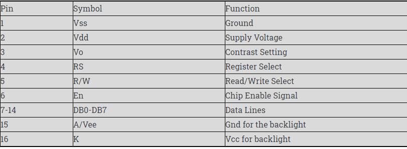
❖ When RS is low (0), the data is to be treated as a command.
❖ When RS is high (1), the data being sent is considered as text data which should be displayed on the screen.
❖ When R/W is low (0), the information on the data bus is being written to the LCD.
❖ When RW is high (1), the program is effectively reading from the LCD.
❖ The ENABLE pin is used to latch the data present on the data pins.
❖ A HIGH - LOW signal is required to latch the data.
❖ The LCD interprets and executes our command at the instant the EN line is brought low.
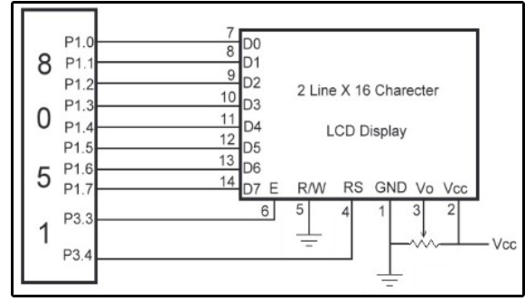
Figure 4. Interfacing of LCD with 8051.
To display a character on LCD we basically write into DDRAM. For a 2x16 LCD the DDRAM address for the first line is from 80h to 8fh & for the second line is 0c0h to 0cfh. So, to display 'H' on the 7th position of the first line then we can write at location 87h.
Data to be displayed

Command or Special Instruction

Write a program to display 'DNA TECHNOLOGY' on LCD.
ORG 0000h
CALL lcd_initialize
CALL lcd_clr
MOV A, #80h //Location from where Data is to be displayed
CALL lcd_command
MOV A, #'D'
CALL lcd_datadisplay
MOV A, #'N'
CALL lcd_datadisplay
MOV A, #'A'
CALL lcd_datadisplay
MOV A, #20h //Hex value for blank space to be displayed
CALL lcd_datadisplay
MOV A, #'T'
CALL lcd_datadisplay
MOV A, #'E'
CALL lcd_datadisplay
MOV A, #'C'
CALL lcd_datadisplay
MOV A, #'H'
CALL lcd_datadisplay
MOV A, #'N'
CALL lcd_datadisplay
MOV A, #'O'
CALL lcd_datadisplay
MOV A, #'L'
CALL lcd_datadisplay
MOV A, #'O'
CALL lcd_datadisplay
MOV A, #'G'
CALL lcd_datadisplay
MOV A, #'Y'
CALL lcd_datadisplay
Stop:
Ajmp stop.
Q20) Explain keyboard interfacing?
A20)
Interfacing of keyboard
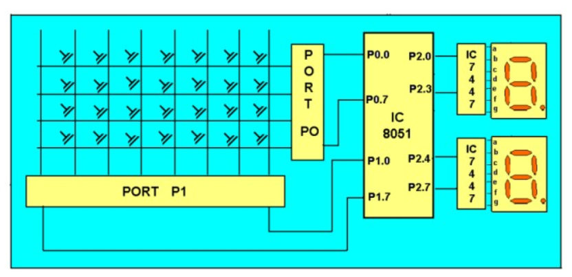
Keyboard Interfacing with 8051.
Working:
❖ The 8051 has 4 I/O ports P0 to P3 each with 8 I/O pins, P0.0 to P0.7, P1.0 to P1.7, P2.0 to P2.7, P3.0 to P3.7. Port P1 acts as an I/P port for microcontroller and port P0 as an O/P port, Port P2 is used for displaying the number of pressed keys.
❖ Make all rows of port P0 high so that it gives a high signal when key is pressed.
❖ Check if any key is pressed by scanning port P1 by checking all the columns for non- zero condition.
❖ If any key is pressed, identify which key is pressed and make one row high at a time.
❖ Initiate a counter to hold the count so that each key is counted.
❖ Check port P1 for nonzero condition. If any nonzero number is there in [accumulator], start column scanning by following step 9.
❖ Otherwise make the next row high in port P1.
❖ Add a count of 08h to the counter to move to the next row by repeating steps from step 6.
❖ If any key pressed is found, the [accumulator] content is rotated right through the carry until carry bit sets, while doing this increment count in the counter till carry is found.
❖ Move the content in the counter to display in data field or to memory location
❖ To repeat the procedures, go to step 2.
Program:
Start of main program:
To check that whether any key is pressed
Start: mov a, #00h
Mov p1, a; making all rows of port p1 zero
Mov a, #0fh
Mov p1, a; making all rows of port p1 high
Press: mov a, p2
Jz press; check until any key is pressed
After making sure that any key is pressed
Mov a, #01h; make one row high at a time
Mov r4, a
Mov r3, #00h; initiating counter
Next: mov a, r4
Mov p1, a; making one row high at a time
Mov a, p2; taking input from port A
Jnz colscan; after getting the row jump to check
Column
Mov a, r4
Rl a; rotate left to check next row
Mov r4, a
Mov a, r3
Add a, #08h; increment counter by 08 count
Mov r3, a
Sjmp next; jump to check next row
After identifying the row to check the column following steps are followed
Colscan: mov r5, #00h
In: rrc a; rotate right with carry until get the carry
Jc out; jump on getting carry
Inc r3; increment one count
Jmp in
Out: mov a, r3
Da a; decimal adjust the contents of counter
Before display
Mov p2, a
Jmp start; repeat for check next key.
Q21) Explain ADC Interfacing?
A21)
ADC0808/0809:
ADC0808/0809 is a monolithic CMOS device which consists of 28 pins and gives 8-bit value in output for 8- channel ADC input pins (IN0-IN7).
It has a resolution of 8 therefore it can encode the analog data into one of the 256 levels (28).
It has three channel address lines namely: ADDA, ADDB and ADDC to select channels.
Pin Diagram for ADC0808
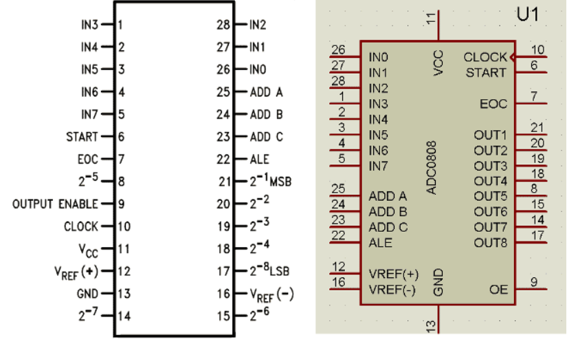
Figure 5. ADC 0808 Pin
ADC0808/0809 needs a clock pulse for conversion which can be provided by using an oscillator or microcontroller.
Select the input channel using address lines, like the input line IN0 by keeping all three address lines (ADDA, ADDB, ADDC) low.
Suppose IN2 is selected to keep ADDA and ADDB low and ADDC high.
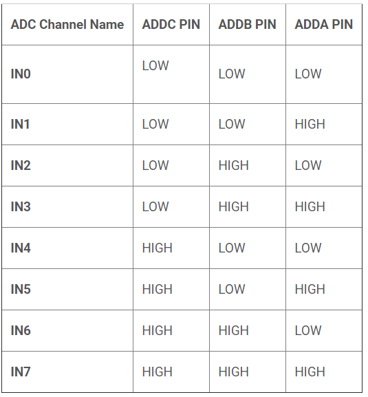
Figure. Channel selection
SOC [Start of conversion]:
When High to low signal is appears on the pin of ADC, and ADC starts conversion

Figure. SOC
EOC [End of conversion]:
To indicate completion of conversion ADC sends a high EOC signal to the microcontroller.
OE [Output Enable]:
When a high signal is applied to this pin, the output latch of ADC is enabled and the converted data is made available to the Microcontroller.
The reference voltage determines the range of analog input voltage.
For example: - If reference voltage is 5V then analog voltage ranges from 0V-5V. If the reference voltage is 2.56V then the range is from 0V-2.56V.
The frequency of the applied clock signal determines conversion speed.
Working:
⮚ Initially, microcontroller provides a 500 KHz clock signal to ADC0808 because the Timer 0 interrupt requires clock signal to operate to operate as ADC.
⮚ Then the microcontroller sends a LOW to HIGH level signal to ALE pin (active-high pin) of ADC0808 to enable the latch in the address.
⮚ By applying HIGH to LOW Level signal to SC (Start Conversion), ADC starts analog to digital conversion. And then wait for the EOC (End of Conversion) pin to go LOW.
⮚ When EOC goes LOW, it means analog to digital conversion has been completed and data is ready to use.
⮚ After this, the microcontroller enables the output line by applying a HIGH to LOW signal to the OE pin of ADC0808.
⮚ ADC0808 gives ratio metric conversion output at its output pins.
Radiometric conversion is given by
Vin/ (Vfs – Vz) = Dx / (Dmax – Dmin)
Where:
Vin is input voltage for conversion
Vfs is full scale voltage
Vz is zero voltage
Dx is data point being measured
Dmax is maximum data limit
Dmin is the minimum data limit.
Interfacing Diagram:
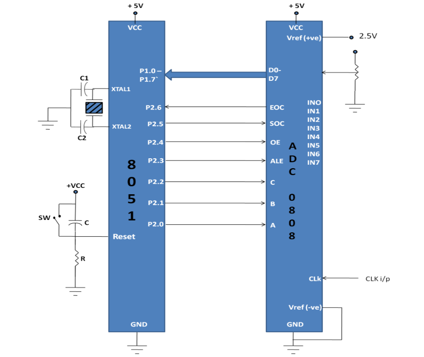
Figure. Interfacing 8051 with ADC0808
Program:
SOC EQU P2.6
EOC EQU P2.5
OE EQU P2.4
ALE EQU P2.3
ADDR_C EQU P2.2
ADDR_B EQU P2.1
ADDR_A EQU P2.0
ORG 0000H
MOV P1, #0FFH
SETB P2.5
CLR SOC
CLR OE
CLR ALE
AGAIN: CLR ADDR_C
CLR ADDR_B
CLR ADDR_A
SETB SOC
SET ALE
ACALL DELAY
CLR SOC
CLR ALE
BACK: JB EOC BACK
HERE: JNB EOC HERE
SETB OE
MOV A, P1
ACALL CONVERSION
ACALL DISPLAY
AGAIN: SJMP AGAIN
Q22) Explain DAC Interfacing?
A22)
DAC
The Digital to Analog converter (DAC) is a device used for converting digital pulses to analog signals.
There are two methods of converting digital signals to analog signals which are binary weighted method and R/2R ladder method.
The MC1408 (DAC0808) Digital to Analog Converter uses the R/2R ladder method. This method can achieve a higher degree of precision. DACs are judged by its resolution., If there are n digital input pins, there are 2n analog levels. So, 8 input DAC has 256 discrete voltage levels.
MC1408 DAC (or DAC0808)
In this chip the digital inputs are converted to current. The output current is known as Iout by connecting a resistor to the output to convert into voltage.
The total current provided by Iout pin is basically a function of binary numbers at the input pins D0 - D7 (D0 is the LSB and D7 is the MSB) of DAC0808 and the reference current Iref.
The following formula is showing the function of Iout
Iout=Iref⟮D7/2+D6/4+D5/8+D4/16+D3/32+D2/64+D1/128+D0/256⟯
The Iref is the input current. This must be provided into the pin 14. Generally, 2.0mA is used as Iref
Generating Sinewave using DAC and 8051 Microcontroller
For generating sinewave first, we need a look-up table to represent the magnitude of the sine value of angles between 0° to 360°. The sine function varies from -1 to +1.
In the table only integer values are applicable for DAC input. In this example we will consider 30° increments and calculate the values from degree to DAC input. We are assuming a full-scale voltage of 10V for DAC output.
We can follow this formula to get the voltage ranges.
Vout = 5V + (5 x sin θ)
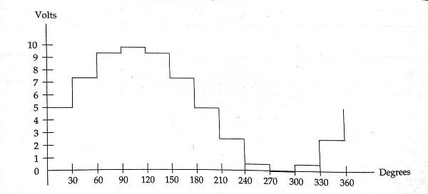
The lookup table according to the angle and other parameters for DAC.
Angle (in θ) | Sinθ | Vout (Voltage Magnitude) | Values sent to DAC |
0 | 0 | 5 | 128 |
30 | 0.5 | 7.5 | 192 |
60 | 0.866 | 0.866 | 9.33 |
90 | 1.0 | 1.0 | 10 |
120 | 0.866 | 0.866 | 9.33 |
150 | 0.5 | 0.5 | 7.5 |
180 | 0 | 0 | 5 |
210 | -0.5 | -0.5 | 2.5 |
240 | -0.866 | -0.866 | 0.669 |
270 | -1.0 | -1.0 | 0 |
300 | -0.866 | -0.866 | 0.669 |
330 | -0.5 | -0.5 | 2.5 |
360 | 0 | 0 | 5 |
Circuit Diagram −
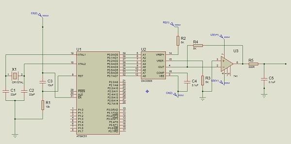
Source Code
#include <reg51.h>
Sfr DAC = 0x80; // Port P0 address
Void main()
{
Int sin value[12] = {128,192,238,255,238,192,128,64,17,0,17,64};
Int i;
While(1){
// infinite loop for LED blinking
For(i=0;i<12;i++)
{
DAC = sin_value[i];
}
}
}
Output
The output will look like this −
Q23) Explain sensor interfacing?
A23)
In case of temperature the Celsius and Fahrenheit scale thermometer displays the ambient temperature through a LCD display.
This consists of two sections:
▪ One senses the temperature. The temperature sensor is LM 35.
▪ The other converts the temperature value into a suitable number in Celsius scale by ADC0804.
The temperature is sensed in Celsius scale and converted into Fahrenheit scale temperature by using Celsius to Fahrenheit conversion formulae.
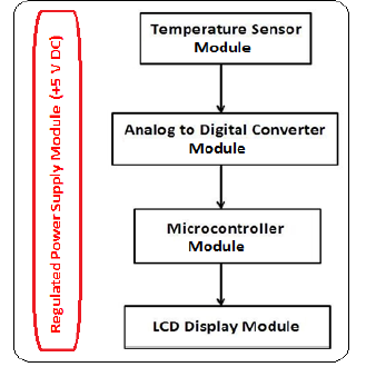
Process
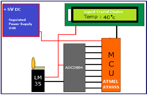
Circuit Diagram
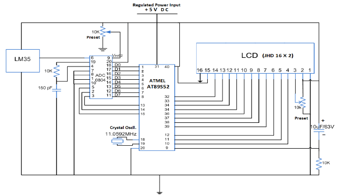
Interfacing of Temperature sensor with microcontroller
- The temperature sensor used is LM35. The LM 35 IC generates a 10mV variation in its output voltage for every degree Celsius change in temperature. The output of the temperature sensor is analog in nature.
- Hence, there is a need for an analog to digital converter to convert the analog input to its equivalent binary output.
- The ADC 0804 is the analog to digital converter IC. It is a single channel converter that converts the analog input up to a range of 5V into its equivalent 8-bit binary output.
- The step size is defined by the voltage applied at Vref/2 pin of the ADC IC.
For example, if the voltage at Vref/2 pin is set to 1.28V then ADC step size will be 10 mV. Similarly, if the input voltage is 1V the equivalent binary output of ADC will be 1000 or 0110, 0100 in binary.
- For every 10mV rise of input voltage the 8-bit binary output of ADC is incremented by one. Different step size can be selected by changing the voltage input to Vref/2 pin.
- The step size of ADC is calibrated by using a preset to match the actual temperature.
- Once ADC is calibrated it provides the correct output.
- The binary output of ADC is fed parallel to the port of the microcontroller. The microcontroller reads the input through ADC and displays its corresponding decimal value on the LCD which indicates temperature.
Program:
ORG 00H
MOV P1, #11111111B // initializes P1 as input port
MOV P0, #00000000B // initializes P0 as output port
MOV P3, #00000000B // initializes P3 as output port
MOV DPTR, #LABEL // loads the address of "LABEL" to DPTR
MAIN: MOV R4, #250D // loads register R4 with 250D
CLR P3.7 // makes Cs=0
SETB P3.6 // makes RD high
CLR P3.5 // makes WR low
SETB P3.5 // low to high pulse to WR for starting conversion
WAIT: JB P3.4, WAIT // polls until INTR=0
CLR P3.7 // ensures CS=0
CLR P3.6 // high to low pulse to RD for reading the data from ADC
MOV A, P1 // moves the digital output of ADC to accumulator A
MOV B, #10D // load B with 10D
DIV AB // divides the content of A with that in B
MOV R6, A // moves the quotient to R6
MOV R7, B // moves the remainder to R7
DLOOP: SETB P3.2 // sets P3.2 which activates LED segment 1
MOV A, R6 // moves the quotient to A
ACALL DISPLAY // calls DISPLAY subroutine
MOV P0, A // moves the content of A to P0
ACALL DELAY // calls the DELAY subroutine
CLR A // clears A
MOV A, R7 // moves the remainder to A
CLR P3.2 // deactivates LED segment 1
SETB P3.1 // activates LED segment 2
ACALL DISPLAY
MOV P0, A
ACALL DELAY
CLR A
CLR P3.1 // deactivates LED segment 2
DJNZ R4, DLOOP // repeats the loop "DLOOP" until R4=0
SJMP MAIN // jumps back to the main loop
DELAY: MOV R3, #255D // produces around 0.8mS delay
LABEL1: DJNZ R3, LABEL1
RET
DISPLAY: MOVC A, @A+DPTR // converts A's content to corresponding digit drive pattern
RET
LABEL: DB 3FH // LUT (look up table) starts here
DB 06H
DB 5BH
DB 4FH
DB 66H
DB 6DH
DB 7DH
DB 07H
DB 7FH
DB 6FH
END
Q24) Explain external memory interfacing?
A24)
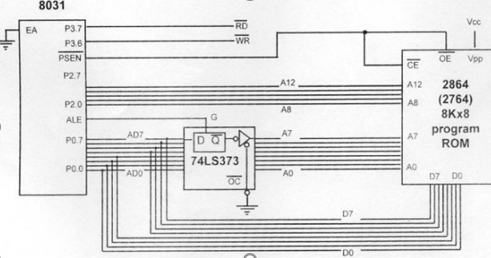
Circuit diagram to interface external program ROM with 8051
Step 1: Connect EA pin to ground
Step 2: Connect the PSEN to the CE and OE.
Step 3: Then, Port 2 (P2.0 – P2.7) to A8 – A12 pins of ext. ROM.
Step 4: Connect ALE to G of 74LS373 latch to enable it.
Step 5: Next, connect the OC of 74LS373 to GND.
Step 6: Connect Port 0 (P0.0 – P0.7), which consists of both address and data multiplexed into Port 0 to 1D – 8D pins of 74LS373 latch to demultiplex it and 1Q – 8Q of the latch to A0 – A7 of ext. ROM.
Step 7: Connect Port 0 (P0.0 – P0.7) to D0 – D7 of the ext. ROM.
Step 8: VPP of ext. ROM to VCC.
ORG 0000H
MOV DPTR, #4000H; Load DPTR with the location where data is stored
MOV R0, #40H; Load R0 with the int RAM loc where you want to save the data
Rep: MOV A, #00H; Clear accumulator
MOVC A, @A+DPTR; Syntax to mode data from ext. ROM to accumulator
MOV @R0, A; Copy the value of accumulator in location pointed by R0
INC R0; Inc R0 to point to next int RAM location
INC DPTR; Inc DPTR to point to next ext. ROM location
CJNE A, #00H, rep; Repeat this process until 0 is received from the DPTR
Stay: SJMP stay; Stay here
END
Circuit diagram to interface external data ROM with 8051
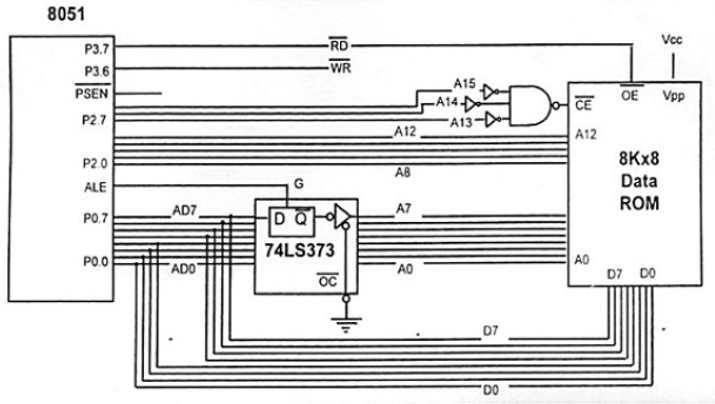
Code to interface external data ROM with 8051
This is an assembly language program to read 100 bytes of data from external data ROM located at 1000H and send it to Port 1 of 8051.
ORG 0000H
MYXDATA EQU 1000H; 1000H, location where data is stored externally
COUNT EQU 100; To receive all 100 bytes of data
MOV DPTR, #MYXDATA; Move DPTR to 1000H location
MOV R0, #COUNT; Load R0 with 100
Rep: MOVX A, @DPTR; Copy data from location pointed by DPTR to acc
MOV P1, A; Move contents of acc to P1
INC DPTR; Inc DPTR to next ROM location
DJNZ R0, rep; Repeat until all 100 bytes are received
Stay: SJMP stay; Stay here forever
END
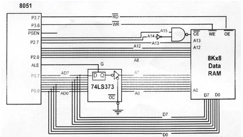
Circuit diagram to interface external RAM with 8051
Step 1: Connect RD to OE of ext. RAM.
Step 2: Connect WR to WE of ext. RAM.
Step 3: Connect active low input of NAND gate to CE of external RAM, where the input to NAND gate is address lines A15, A14, and A13. We’ve given 0 1 0 to these lines to access the 8000H location of the external RAM.
Circuit diagram to interface external data RAM to 8051
Code to interface external RAM with 8051
This is an assembly language program to send 150 bytes of data or status of Port 2 to external RAM located at 6000H.
First of all, to access 6000H of the data memory, we have to send 0 1 1 to A15 A14 A13 respectively.
ORG 0000H
RAMLOC EQU 6000H; External RAM location = 6000H
COUNT EQU 150; Variable count = 150d
MOV DPTR, #RAMLOC; Mov DPTR to point to ext. RAM location
MOV R3, #COUNT; Number of bytes of data
Rep: MOV A, P1; Copy status of P2 into acc
MOVX @DPTR, A; Copy the content of acc to the ext. RAM
ACALL DELAY; call a delay before repeating the process
INC DPTR; Inc DPTR to point to next location
DJNZ R3, rep; Repeat this until all the bytes of data are sent
Stay: SJMP stay; Stay here forever
END
Interfacing external program ROM, data ROM and external RAM with the 8051
To interface both program ROM and data RAM to 8051, Let’s say we want to interface 16KB data RAM, 16KB program ROM, and 16KB of data RAM, then use the following steps:
Step 1: Calculate the number of address lines required to access 16KB of data, that is 214 = 16KB. Here, we require 14 address lines A0 – A13.
Step 2: Decide the location of RAM and ROM, here we are going to interface program ROM from 0000H and data RAM from 8000H.
Step 3: Select the decoder circuit, here we’re going to select 74LS138 decoder.
Step 4: We do not need a decoder circuit for program ROM, but we have to connect the 74LS138 decoder to data ROM and data RAM.
Step 5: Connect G1 to VCC, G2A, and G2B to ground.
Step 6: Connect input A and B to P2.6 and P2.7 respectively, and the input C to ground.
Step 7: We connect external program and data ROM, for that we can use an AND gate with its input being signal from RD (to access external data space) and PSEN (to access external program space) and output to OE of external ROM.
Step 8: To interface the external RAM, we connect both RD and WR to WE and OE respectively of external RAM.
