Unit-5
Fundamentals of Communication Engineering
Q1) What are the elements of a Communication System.
A1)

Fig. 1 Block diagram of elements of communication (ref 3)
Information Source
It produces a message that is analog in nature, i.e., the output of the information source is a continuous signal.
Analog carrier source
Sine wave is used as a carrier signal which will help in analog modulation.
Analog modulation
The carrier signal is superimposed with the message signal and then the modulated signal is obtained which is also analog in nature.
Communication channel
The analog modulated signal is transmitted via the communication channel towards the receiver end after addition of the requisite power levels.
Analog demodulation
At the receiver end, the incoming modulated signal is passed through an analog demodulation process which extracts the analog message signal. The analog message is then passed onto the final destination.
Destination
The nature of signal starting from the information source till the final destination is analog.
Q2) Explain various frequencies with the help of diagram.
A2)
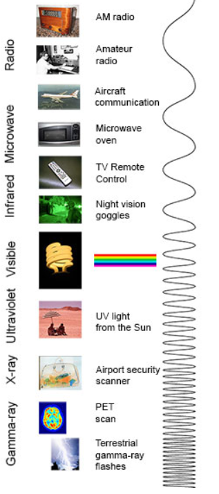
Radio: Your radio captures radio waves emitted by radio stations, bringing your favourite tunes. Radio waves are also emitted by stars and gases in space.
Microwave: Microwave radiation will cook your popcorn in just a few minutes, but is also used by astronomers to learn about the structure of nearby galaxies.
Infrared: Night vision goggles pick up the infrared light emitted by our skin and objects with heat. In space, infrared light helps us map the dust between stars.
Visible: Our eyes detect visible light. Fireflies, light bulbs, and stars all emit visible light.
Ultraviolet: Ultraviolet radiation is emitted by the Sun and are the reason skin tans and burns. "Hot" objects in space emit UV radiation as well.
X-ray: A dentist uses X-rays to image your teeth, and airport security uses them to see through your bag. Hot gases in the Universe also emit X-rays.
Gamma ray: Doctors use gamma-ray imaging to see inside your body. The biggest gamma-ray generator of all is the Universe.
Q3) What is the Need of modulation.
A3)
1>. Antenna height reduces
2>. Avoids mixing of signal
3>. Increases the range of communication [ In Kilometers]
4>. Multiplexing of signals is possible
5>. Improves quality of reception of signal.
1>. Antenna height Reduces: - Antenna theory specifies that the height of the antenna required for radiation of radio waves is a function of wavelength of the frequency fed at the i/p of the antenna. Antenna height must be multiple of ( d/4 ),
Where ‘ d ‘ is the wavelength.
d = speed of light / frequency of signal
d = c / f = 3 x 10⁸ / f
eg : Consider the voice as analog baseband signal with f = 4 KHz
d = 3 x 10⁸ / 4 x 10³
d = 75 x 103 m
d = 75 km
Height of antenna required is d / 4
= 75 km / 4 = 18.75 km
2>. Increase range of communication: - The frequency of baseband signal is low. At low frequency the signal radiation from antenna is poor or weak. Due to this reason the signal gets attenuated and can’t travel long distance when it is transmitted.
Attenuation of the transmitted signal reduces when the frequency is increased.
Thus modulation increases the frequency of the signal to be radiated. Thus, increase in frequency increases the range of communication.
Q4) Practically you cannot build the antenna of 18.7 km height. Consider this voice signal of 4 kHz frequency is used to modulate the carrier signal of 2 MHz frequency.
A4) F = 2 MHz
D = c / f = 3 x 10⁸ / 2 x 106 = 150 m
Minimum height of antenna required = d / 4 = 150 / 4 = 37.5 m
Therefore, antenna height required for radio communication reduces from 75 km to 37.5 meters due to modulation.
Q5) A modulating signal m(t)=10cos(2π×103t)m(t) is amplitude modulated with a carrier signal c(t)=50cos(2π×105t). Find the modulation index, the carrier power, and the power required for transmitting AM wave.
A5) Given, the equation of modulating signal as
m(t)=10cos(2π×103t)m(t)
We know the standard equation of modulating signal as
m(t)=Amcos(2πfmt)m(t)
By comparing the above two equations, we will get
Am=10volts
and Frequency of modulating signal as
fm=103Hz=1KHz
Given, the equation of carrier signal is
c(t)=50cos(2π×105t))
The standard equation of carrier signal is
c(t)=Accos(2πfct)c(t)
By comparing these two equations, we will get
Amplitude of carrier signal as Ac=50voltsAc
and Frequency of carrier signal as fc=105Hz=100KHz
We know the formula for modulation index as
μ=Am/Ac
μ=10/50=0.2
Therefore, the value of modulation index is 0.2 and percentage of modulation is 20%.
The formula for Carrier power, Pc
Pc=Ac2 /2R
Assume R=1ΩR=1Ω and substitute Ac value in the above formula.
Pc=(50)2/2(1)=1250W
Therefore, the Carrier power, Pc is 1250 watts.
We know the formula for power required for transmitting AM wave is
Pt=Pc(1+μ2/2)
Pt=1250(1+(0.2)22)=1275W
Therefore, the power required for transmitting AM wave is 1275 watts
Q6) Explain Balanced Modulator (Product Modulator).
A6) A balanced modulator consists of two standard amplitude modulators arranged in a balanced configuration so as to suppress the carrier wave as shown in the following block diagram. It is assumed that the AM modulators are identical, except for the sign reversal of the modulating wave applied to the input of one of them. Thus, the output of the two modulators may be expressed as,
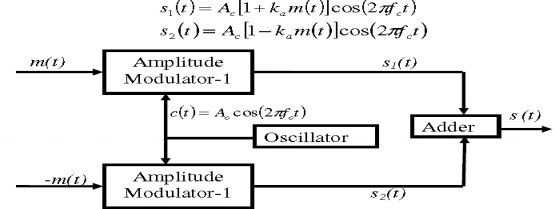
Balanced Modulator
Subtracting s2(t) from s1(t) we get
s(t) = s1(t) – s2(t)
s(t) = 2 ka m(t) cos(2πfct)
Hence, except for the scaling factor 2ka, the balanced modulator output is equal to the product of the modulating wave and the carrier.
Q7) Draw and explain Ring Modulator.
A7)
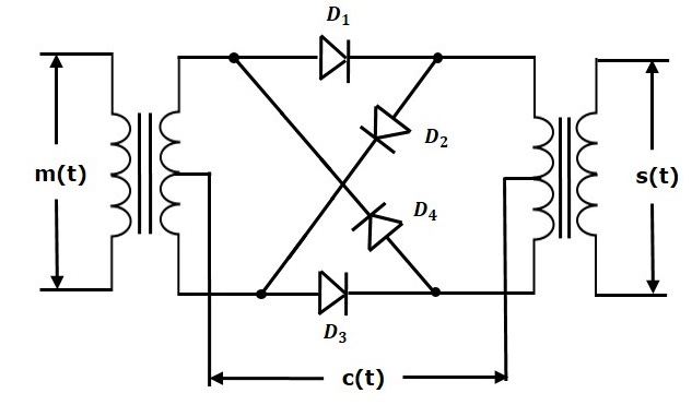
Operation
From the above analysis, we can say that the four diodes D1, D2, D3 and D4 are controlled by the carrier signal.
If the carrier is a square wave, then the Fourier series representation of c(t) is given by
c(t) = 4 / π  n-1 / 2n -1 cos[2πfct(2n−1)]
We will get DSBSC wave s(t) which is just the product of the carrier signal c(t)) and the message signal m(t) i.e.,
s(t) = 4 / π  n-1 / 2n -1 cos[2πfct(2n−1)] m(t)
the ring modulator.
DSBSC modulators are known as product modulators as they produce the output, which is the product of two input signals.
Q8) Explain Balanced Modulator using Non-linear resistance.
A8)
As indicated in the Figure, the input voltage at diode D1 is vc+vm and input voltage at diode D2 is vc−vm.
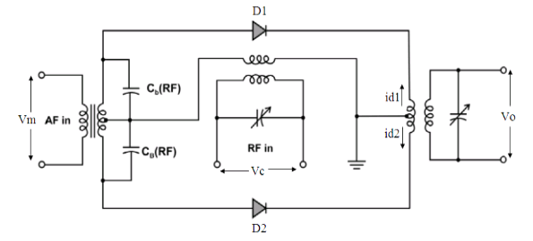
The primary current of the output transformer is i1=id1−id2.
where,
id1=a+ b(vc+vm)+ c(vc+vm)2
id2=a+ b(vc−vm)+c(vc−vm)2
Thus, we get,
i1= id1−id2=2bvm+4cvmvc
The modulating and carrier voltage are represented as,
vm=Vm sinωmt and vc=Vc sinωct
Substituting for vm and vc and simplifying, we get,
i1=2bVmsinωmt+4cmVc/2cos(ωc−ωm)t−4cmVc/2cos(ωc+ωm)t
The output voltage v0 is proportional to primary current i1 and assume constant of proportionality as α, which can be expressed as,
v0=αi1=2αbVmsinωmt+4αcmVc/2cos(ωc−ωm)t−4αcmVc/2cos(ωc+ωm)t
Let P=2αbVmP and Q=2αcmVc2.
Thus we have,
v0=Psinωmt+2Qcos(ωc−ωm)t−2Qcos(ωc+ωm)t
The above equation shows that carrier has been cancelled out , leaving only two
sidebands and the modulating frequencies from the output is eliminated by the tuning of the output transformer, which results in the below equation of the generated DSBSC wave.
v0=2Qcos(ωc−ωm)t−2Qcos(ωc+ωm)t
Q9) Explain Switching Modulator in detail.
A9)
.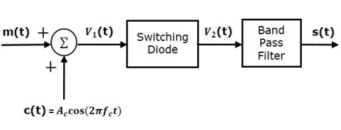
Switching modulator is similar to the square law modulator. The only difference is that in the square law modulator, the diode is operated in a non-linear mode, whereas, in the switching modulator, the diode has to operate as an ideal switch.
Let the modulating and carrier signals be denoted as m(t) and c(t)=Ac cos(2πfct). These two signals are applied as inputs to the summer (adder) block. Summer block produces an output, which is the addition of modulating and carrier signals. Mathematically, we can write it as
V1(t)=m(t)+c(t)=m(t)+Ac cos(2πfct)
This signal V1(t) is applied as an input of diode.
Assume, the magnitude of the modulating signal is very small when compared to the amplitude of carrier signal Ac. So, the diode’s ON and OFF action is controlled by carrier signal c(t). This means, the diode will be forward biased when c(t)>0 and it will be reverse biased when c(t)<0.
Therefore, the output of the diode is
V2(t)={V1(t)0 if c(t)>0
0 c(t) <0
We can approximate this as
V2(t)=V1(t)x(t)
Where, x(t) is a periodic pulse train with time period T=1fc

The Fourier series representation of this periodic pulse train is
x(t)=1/ 2+2π  n -1 / 2n-1 cos( 2π(2n-1) fc(t))---------------------(1)
= ½ + 2/π cos(2πfct) -2 / 3 π cos(6πfct)+ ………… ----------------(2)
Substituting V1(t) and x(t) we get
V2(t) = [m(t) + Ac cos(2πfct) ] [½ + 2/π cos(2πfct) -2 / 3 π cos(6πfct)+ …………]---------------------------------------(3)
V2(t) = Ac/2 (1+ 4/πAc)m(t) cos(2πfct) + m(t)/2 + 2Ac/π cos (2πfct)- 2m(t)/3π cos(6 πfct)- 2A/3π cos(2πfct) cos(6πfct) + ………………………….
The 1st term of the above equation represents the desired AM wave and the remaining terms are unwanted terms. Thus, with the help of band pass filter, we can pass only AM wave and eliminate the remaining terms.
Therefore, the output of switching modulator is
s(t)=Ac2(1+(4π/Ac)m(t))cos(2πfct)
We know the standard equation of AM wave is
s(t)=Ac[1+kam(t)]cos(2πfct)s(t)
Where, ka is the amplitude sensitivity.
By comparing the output of the switching modulator with the standard equation of AM wave, we will get the scaling factor as 0.5 and amplitude sensitivity ka as 4π/Ac.
Q10) Write a short note on SSB-SC.
A10) The process of suppressing one of the sidebands along with the carrier and transmitting a single sideband is called as Single Sideband Suppressed Carrier system or simply SSBSC. It is plotted as shown in the following figure.
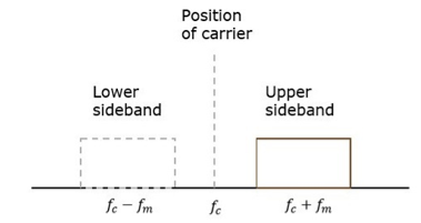
Carrier and sideband are suppressed and single sideband is allowed for transmission.
Let us consider the
Modulating signal
m(t)=Am cos(2πfmt)
Carrier signal
c(t)=Ac cos(2πfct)
Mathematically, we can represent the equation of SSB-SC wave as
s(t)=AmAc2cos[2π(fc+fm)t] for the upper sideband
Or
s(t)= AmAc2cos[2π(fc−fm)t] for the lower sideband
Bandwidth of SSB-SC Wave
We know that the DSB-SC modulated wave contains two sidebands and its bandwidth is 2fm. Since the SSB-SC modulated wave contains only one sideband, its bandwidth is half of the bandwidth of DSBSC modulated wave.
i.e., Bandwidth of SSBSC modulated wave =2fm/2=fm
Therefore, the bandwidth of SSB-SC modulated wave is fm and it is equal to the frequency of the modulating signal.
Power Calculations of SSB-SC Wave
Consider the following equation of SSBSC modulated wave.
s(t)=AmAc/2 cos[2π(fc+fm)t] for the upper sideband
Or
s(t)=AmAc/2 cos[2π(fc−fm)t] for the lower sideband
Power of SSB-SC wave is equal to the power of any one sideband frequency components.
Pt=PUSB=PLSB
We know power
P=vrms2 / R
=(vm/√2)2 / R
In this case, the power of the upper sideband is
PUSB=(AmAc/2√2)2 / R = Am2Ac2 /8R.
Similarly, for lower sideband power.
PLSB=Am2Ac2 / 8R
Therefore, the power of SSB-SC wave is
Pt=Am2Ac2 / 8R
Advantages
Disadvantages
Applications
Q11) Explain the Generation of SSB-SC by Frequency Discrimination Method.
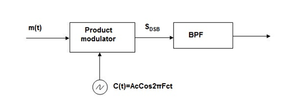
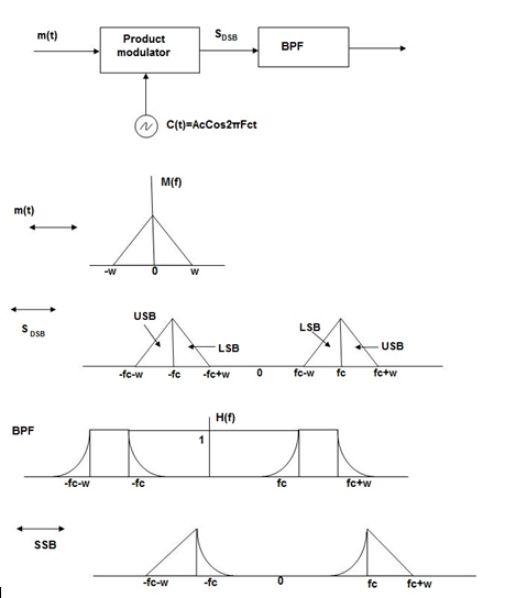
A11) In this method the DSB signal is passed through band pass filter to generate SSB signal.
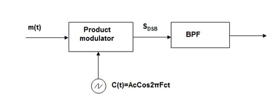
The center frequency of the band pass signal decides whether USB or LSB signal is generated.
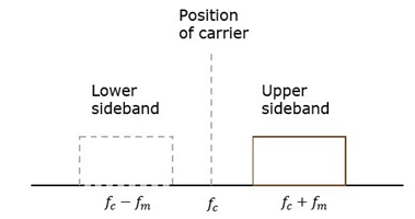
Suppose we want to transmit USB then using band pass filter with center frequency fc + w/2 we obtain the desired result as shown in the figure.
Q12) Explain the Generation of SSB-SC by Phase Discriminated Method.
A12) Consider the following block diagram of SSB-SC modulator using phase discrimination method.
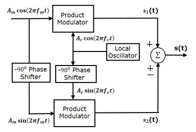
The modulating signal
m(t) = Am cos(2πfmt) -----------------(1)
the carrier signal
c(t) = Ac cos(2πfct) -----------------------(2)
which are directly applied as inputs to the upper product modulator. So, the upper product
modulator produces an output, which is the product of these two inputs.
The output of upper product modulator is
s1(t)=AmAc cos(2πfmt)cos(2πfct) --------------------(3)
s1(t)=AmAc/2{cos[2π(fc+fm)t]+cos[2π(fc−fm)t]} -----------(4)
The modulating signal Am cos(2πfmt) and the carrier signal Ac cos(2πfct) are phase shifted by −900 before applying as inputs to the lower product modulator. So, the lower product modulator produces an output, which is the product of these two inputs.
The output of lower product modulator is
s2(t)=AmAc cos(2πfmt−900)cos(2πfct−900) ---------------(5)
s2(t)=AmAc sin(2πfmt) sin(2πfct) -------------------(6)
s2(t)=AmAc/2{cos[2π(fc−fm)t]−cos[2π(fc+fm)t]} ----------(7)
Add s1(t) and s2(t) in order to get the SSB-SC modulated wave s(t) having a lower sideband.
s(t)=AmAc/2{cos[2π(fc+fm)t]+cos[2π(fc−fm)t]}+AmAc/2{cos[2π(fc−fm)t]−cos[2π(fc+fm)t]} ----------------------------------(8)
s(t)=AmAc cos[2π(fc−fm)t] ------------------------(9)
Subtract s2(t) from s1(t) in order to get the SSBSC modulated wave s(t) having a upper sideband.
s(t)=AmAc/2{cos[2π(fc+fm)t]+cos[2π(fc−fm)t]}−AmAc/2{cos[2π(fc−fm)t]−cos[2π(fc+fm)t]} ---------------------------------------------------------(10)
s(t)=AmAc cos[2π(fc+fm)t] --------------------------(11)
Hence, by properly choosing the polarities of inputs at summer block, we will get SSB-SC wave having a upper sideband or a lower sideband.
Q13) Explain VSB (Vestigial Side Band Suppressed Carrier).
A13) We can get one sideband frequency component completely by using an ideal band pass filter. However, practically we may not get the entire sideband frequency component. Because of this, some information gets lost.
To avoid this loss, a technique is chosen, which is a compromise between DSBSC and SSBSC. This technique is known as Vestigial Side Band Suppressed Carrier (VSBSC) technique. The word “vestige” means “a part” from which, the name is derived.
VSBSC Modulation is the process, where a part of the signal called as vestige is modulated along with one sideband. The frequency spectrum of VSBSC wave is shown in the figure.
Along with the upper sideband, a part of the lower sideband is also transmitted in this technique. Similarly, we can transmit the lower sideband along with a part of the upper sideband. A guard band of very small width is laid on either side of VSB in order to avoid the interferences. VSB modulation is mostly used in television transmissions.
Bandwidth of VSBSC Modulation
We know that the bandwidth of SSBSC modulated wave is fm. Since the VSBSC modulated wave contains the frequency components of one side band along with the vestige of other sideband, the bandwidth of it will be the sum of the bandwidth of SSBSC modulated wave and vestige frequency fv.
Therefore,
Bandwidth of VSBSC Modulated Wave = fm+fv
Advantages
Disadvantages
Applications
The most prominent and standard application of VSBSC is for the transmission of television signals. This is the most convenient and efficient technique when bandwidth usage is considered.
Q14) Explain Generation of VSBSC.
A14) Generation of VSBSC wave is similar to the generation of SSBSC wave. The VSBSC modulator is shown in the following figure.
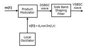
In this method, first we will generate DSBSC wave with the help of the product modulator. Then, apply this DSBSC wave as an input of sideband shaping filter. This filter produces an output, which is VSBSC wave.
The modulating signal m(t)) and carrier signal Ac cos(2πfct) are applied as inputs to the product modulator. Hence, the product modulator produces an output, which is the product of these two inputs.
Therefore, the output of the product modulator is
p(t)=Ac cos(2πfct)m(t)------------------------(1)
Apply Fourier transform on both sides
P(f)=Ac/2[M(f−fc)+M(f+fc)]-------------------(2)
The above equation represents the equation of DSBSC frequency spectrum.
Let the transfer function of the sideband shaping filter be H(f). This filter has the input p(t) and the output is VSBSC modulated wave s(t). The Fourier transforms of p(t) and s(t) are P(f) and S(f) respectively.
Mathematically, we can write
S(f)= =P(f)H(f)------------------(3)
Substitute P(f) value in the above equation.
S(f)=Ac/2[M(f−fc)+M(f+fc)]H(f)-----------------------------(4)
The above equation represents the equation of VSBSC frequency spectrum.
Q15) Explain Demodulation of VSBSC.
A15) Demodulation of VSBSC wave is similar to the demodulation of SSBSC wave. Here, the same carrier signal used for generating VSBSC wave is used to detect the message signal. Hence, this process of detection is called as coherent or synchronous detection. The VSBSC demodulator is shown in the following figure.
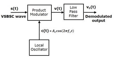
In this process, the message signal can be extracted from VSBSC wave by multiplying it with a carrier, which is having the same frequency and the phase of the carrier used in VSBSC modulation. The resulting signal is then passed through a Low Pass Filter. The output of this filter is the desired message signal.
Let the VSBSC wave be s(t) and the carrier signal is Ac cos(2πfct)
From the figure, we can write the output of the product modulator as
v(t)=Ac cos(2πfct)s(t)----------------------(1)
Apply Fourier transform on both sides
V(f)=Ac/2[S(f−fc)+S(f+fc)]--------------------------(2)
We know that
S(f)=Ac/2[M(f−fc)+M(f+fc)]H(f)-------------------------(3)
From the above equation, let us find S(f−fc )and S(f+fc).
S(f−fc)=Ac/2[M(f−fc−fc)+M(f−fc+fc)]H(f−fc)-----------------------------(4)
S(f−fc)=Ac/2[M(f−2fc)+M(f)]H(f−fc)------------------------------------(5)
S(f+fc)=Ac/2[M(f+fc−fc)+M(f+fc+fc)]H(f+fc)--------------- (6)
S(f+fc)=Ac/2[M(f)+M(f+2fc)]H(f+fc)---------------------------(7)
Substitute, S(f−fc) and S(f+fc) values in V(f)
V(f)=Ac/2[Ac/2[M(f−2fc)+M(f)]H(f−fc)+ Ac/2[M(f)+M(f+2fc)]H(f+fc)] ------------------------(8)
V(f)=Ac2 /4{M(f)[H(f−fc)+H(f+fc)]+Ac2 /4[M(f−2fc)H(f−fc)+M(f+2fc)H(f+fc)]--------------(9)
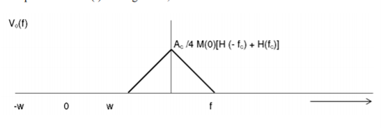
In the above equation, the first term represents the scaled version of the desired message signal frequency spectrum. It can be extracted by passing the above signal through a low pass filter.
V0(f)=Ac2 /4{M(f)[H(f−fc)+H(f+fc)]}-----------------------------------------(10)
Q16) Comparison between SSB, DSB,VSB.
SL No | Parameter | SSB | DSB-SC | VSB |
1 | Power | Less | Medium | Less than DSB_SC |
2 | Bandwidth | Fm | 2fm | fm<BW<2fm |
3 | Carrier Suppression | Yes | Yes | No |
4 | Receiver Complexity | Complex | Complex | Simple |
5 | Application | Point to point communication | Point to Point Communication | Television Broadcasting |
6 | Modulation Type | Linear | Linear | Linear |
7 | Sideband Suppression | One sided completely | No | One sideband suppressed partly |
8 | Transmission Efficiency | Maximum | Moderate | Moderate |