|
|
|
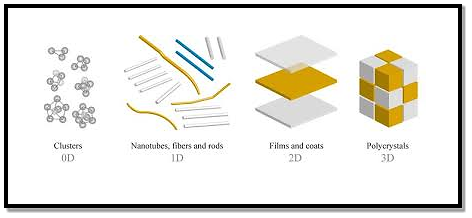
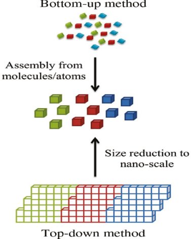
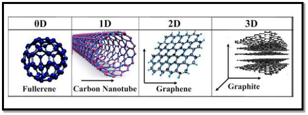
In the past two decades, hundreds of novel NSMs (nanostructured materials) have been obtained therefore, the need for their classification becomes important. NSMs as a subject of nanotechnology are low dimensional materials comprising of building units of a submicron or nanoscale size at least in one direction, and exhibiting size effects. The first classification idea of NSMs was given by Gleiter in 1995, and further was explained by Skorokhod in 2000. However, Gleiter and Skorokhod scheme was not fully considered because 0D, 1D, 2D, and 3D structures such as fullerenes, nanotubes, and nanoflowers were not taken into account. After that, Pokropivny, and Skorokhod reported a modified classification scheme for NSMs, in which 0D, 1D, 2D, and 3D NSMs are included.
0D Nanostructured Materials In the past 10 years, significant progress has been made in the field of 0D NSMs. 0D NSMs such as uniform particle arrays (quantum dots), heterogeneous particle arrays, core-shell quantum dots, onions, hollow spheres, and nano lenses have been synthesized by several research groups. 0D NSMs, such as quantum dots have been extensively studied in light-emitting diodes (LEDs), solar cells, single-electron transistors, and lasers. A 0D structure is the simplest block that can be used for the design of nanomaterials. In this case, the three dimensions are in the nanometre regime and have a diameter of less than 100 nm. Nanoparticles, nanocrystals, and nanoclusters correspond to this group. Nanoparticles They are nanostructures usually used to define all 0D nanostructures or those that are amorphous and have an irregular shape. So, the nanoparticles can be of natural origin, semiconductor, metal, oxides, fullerenes, or quantum dots.
During manufacturing, the nanoparticles that make up the nanomaterials can be of different sizes, which can vary by more than 15%, and still form the nanomaterial without affecting its design. 3D nanomaterials should not be included in the category of nanostructures unless their internal structure is nanostructured. Nanoclusters As well as the nanoparticles, they have an irregular structure besides being semi-crystalline, but they are tinier than the nanoparticles. Its diameter ranges between 1, and 10 nm. Also, nanoclusters are sensitive to their size and become more reactive if they increase or decrease proportionally. Nanocrystals They are monocrystalline nanostructures, whose size ranges from 1 to 30 nm. Semiconductor nanocrystals are more commonly known as quantum dots.
In the last decade, 1D NSMs have stimulated an increasing interest due to their importance in research, and developments, and have a wide range of potential applications. It is generally accepted that 1D NSMs are ideal systems for exploring a large number of novel phenomena at the nanoscale and investigating the size, and dimensionality dependence of functional properties. They are also expected to play an important role as both interconnects, and the key units in fabricating electronic, optoelectronic, and EEDs with nanoscale dimensions. The field of 1D NSMs such as nanotubes has attained significant attention. 1D NSMs have a profound impact on nanoelectronics, nanodevices, and systems, nanocomposite materials, alternative energy resources, and national security. We show the 1D NSMs, such as nanowires, nanorods, nanotubes, nanobelts, nanoribbons, and hierarchical nanostructures, which have been synthesized in the laboratories. They have a variable length, conserving two dimensions (height, and width) in the nanometer regime; to these correspond the nanowires and nanotubes. Nanowires They are elongated crystalline structures whose characteristics stand out for their conductive or semiconducting properties. Nanowires have been obtained from various metallic materials, semiconductors, oxides, etc. In recent years, nanowires have shown special scientific interest due to their potential applications in nanoelectronics, optoelectronics, and sensors. Nanotubes They are tubular structures with a hollow interior. There are nanotubes synthesized, and characterized by inorganic laminar materials. However, the most studied are carbon nanotubes (CNT's).
Two-dimensional nanomaterials (2D) 2D nanostructures have two dimensions outside of the nanometric size range. In recent years, a synthesis of 2D NSMs has become a focal area in materials research, owing to their many low dimensional characteristics different from the bulk properties. In the search for 2D NSMs, considerable research attention has been focused over the past few years on the development of 2D NSMs. 2DNSMs with certain geometries exhibit unique shape-dependent characteristics and subsequent utilization as building blocks for the key components of nanodevices. Besides, a 2D NSMs are particularly interesting not only for a basic understanding of the mechanism of nanostructure growth, but also for investigation, and developing novel applications in sensors, photocatalysts, nano-containers, nanoreactors, and templates for 2D structures of other materials. There are 2D NSMs such as junctions (continuous islands), branched structures, nano-prisms, nanoplates, nanosheets, nanowalls, and nanodisks. They are nanomaterials formed by very thin layers; thin nanolayers with areas of undefined size, and a thickness between 1, and 100 nm. Graphene is the most notable example because, due to its multiple, and exceptional properties, it has the potential to revolutionize technology. Its possible applications extend to very diverse areas, ranging from the miniaturization of electronic devices to the elaboration of drugs against cancer in medicine. |
|
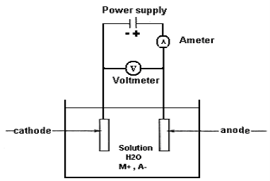
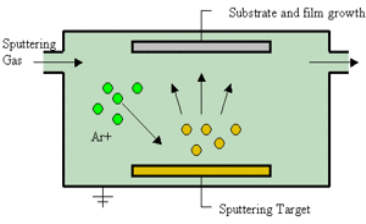
Sputtering Sputtering is a physical process in which atoms in a solid-state (target) are released and pass into the gas phase by bombardment with energetic ions (mainly noble gas ions). Sputtering is usually understood as the sputter deposition, a high vacuum-based coating technique belonging to the group of PVD processes. Sputtering is used as a cleaning method for the preparation of high-purity surfaces and it is also used for analyzing the chemical composition of surfaces. Sputtering is a mechanism by which atoms are dislodged from the surface of a material as a result of a collision with high-energy particles. Thus, PVD by Sputtering is a term used to refer to a physical vapor deposition (PVD) technique wherein atoms or molecules are ejected from a target material by high-energy particle bombardment so that the ejected atoms or molecules can condense on a substrate as a thin film nano dimension. Sputtering has become one of the most widely used techniques for depositing various metallic films on wafers, including aluminum, aluminum alloys, platinum, gold, TiW, and tungsten. Process of Sputtering The principle of Sputtering is to use the energy of plasma (partially ionized gas) on the surface of a target (cathode), to pull the atoms of the material one by one and deposit them on the substrate. Sputtering as a deposition technique may be described as a sequence of these steps: 1) Ions are generated and directed at a target material; 2) The ions sputter atoms from the target; 3) The sputtered atoms get transported to the substrate through a region of reduced pressure; and 4) The sputtered atoms condense on the substrate, forming a thin film. To do this, plasma is created by the ionization of pure gas. Usually, we take Argon gas. Ionization of a pure gas is done by applying potential difference (pulsed DC), or by electromagnetic excitation. Thus plasma is composed of Ar+ ions which are accelerated and confined around the target due to the presence of a magnetic field. Each ionized atom strikes the target and transfers its energy and rips an atom, having enough energy to be projected to the substrate.
Figure 7
The plasma is created at relatively high pressures (10-1 - 10-3 mbar), but it is necessary to start from a lower pressure before the introduction of Argon, to avoid contamination due to the residual gases. The diversity of sputtering target shapes (circular, rectangular, Delta, tubular...) and the materials used allows creating all types of thin layers, including alloys during a single run. Basics of the Sputtering Process When bombarding a surface with ions, various effects may occur, depending on the ions used and their kinetic energy: 1. Material is removed from the bombarded target (cathode). This is the sputtering described here. 2. The ions are incorporated into the target material and enter there, possibly a chemical compound. This effect is then called (reactive) ion implantation. 3. The ions condense on the bombarded substrate, where they form a layer: ion beam deposition. If a material removal is intended, the ions must have a certain minimum energy. The impinging ion transmits its impulse to atoms of the bombarded material (target), which then - similar to the billiards - trigger further collisions. After several collisions, some of the target atoms have a momentum away from the target interior. If such an atom is sufficiently close to the surface and has sufficiently high energy, it leaves the target. The sputter yield depends
To eject an atom from the target, the ions must have material-dependent minimum energy (typically 30-50 eV). Above this threshold, the yield increases. However, initially, it increases strongly then flattens rapidly. At high ion energies, this energy is deposited even deeper into the target and thus barely reaches the surface. The ratio of the masses of ion and target atom determines the possible momentum transfer. For light target atoms, maximum yield is achieved when the mass of target and ion approximately match. However, as the mass of the target atoms increases, the maximum of the yield shifts to ever higher mass ratios between the ion and the target atom. The ion bombardment generates not only neutral atoms, but also secondary electrons and, to a lesser extent, secondary ions and clusters of different masses. The energy distribution of the dissolved atoms has a maximum at half the surface binding energy but falls to high energies only slowly so that the average energy is often an order of magnitude above. This effect is exploited in analysis methods of surface physics and thin-film technology as well as for the production of thin layers (sputter deposition). Advantages 1) Sputtering can be achieved from large-size targets, simplifying the deposition of a thin film with uniform thickness over large wafers; 2) Film thickness is easily controlled by fixing the operating parameters and simply adjusting the deposition time; 3) Control of the alloy composition, as well as other film properties such as step coverage and grain structure, is more easily accomplished than by deposition through evaporation; 4) Sputter-cleaning of the substrate in a vacuum before film deposition can be done; 5) Device damage from X-rays generated by electron beam evaporation is avoided. Disadvantages 1) High capital expenses are required; 2) The rates of deposition of some materials (such as SiO2) are relatively low; 3) Some materials such as organic solids are easily degraded by ionic bombardment; 4) Sputtering has a greater tendency to introduce impurities in the substrate than deposition by evaporation because the former operates under a lesser vacuum range than the latter. |
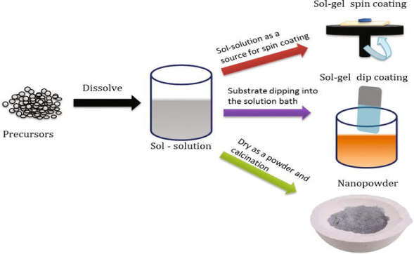
SOL-GEL PROCESS Sol-gel is a low temperature, highly controllable, and cost-effective method for the production of homogeneous, highly stoichiometric, and high-quality ultrafine nanostructures. The sol-gel process involves the formation of a colloidal suspension of particles called “sol", and the transition of the colloidal “sol" into a solid called the "gel" phase. The sol-gel process allows the fabrication of thin films with a large variety of properties. Sol-gel chemistry is a remarkably versatile approach for fabricating materials. The sol is made of solid particles of a diameter of a few hundred nm, usually, inorganic metal salts, suspended in a liquid phase. In a typical sol-gel process, the precursor is subjected to a series of hydrolysis, and polymerization reactions to form a colloidal suspension, and then the particles condense in a new phase, the gel, in which a solid macromolecule is immersed in a solvent. Sol is obtained by either hydrolysis or polymerization reactions by adding suitable reagents in the precursor solution. The sol can be deposited onto preferred substrates as thin films using two techniques, (1) spin coating (2) dip coating The gelation process done through condensation of the sol or the addition of polymers converts this sol to gel. This gel can be used to form materials of different types such as nanoparticles, xerogel, glass, or ceramics depending upon the further processing steps involved.
Figure 8: Schematic diagram of sol-gel processing. Nanoparticles and xerogels can be obtained by simple evaporation of the solvent. The obtained xerogel can be formed as ceramics by heat treatment, and glassy nature can be induced by melting techniques. Thus, the sol-gel method can be used to obtain different forms of materials, controlled phase, and shape, and size of the derived materials The parameters that could be controlled in the sol-gel method includes (1) Concentration of precursor used, (2) Nature of solvent used, (3) the pH of the solution, (4) Type of additives added, and their concentration, (5) Pre, and post-heat treatment of the materials, (6) Aging of the solution, and (7) Nature of polymer used for condensation The particles formed in the gel matrix possess uniform shape, and size that enhances the optical, electrical, magnetic, and other intrinsic nature of the materials. Of the factors listed above, pH, nature, and concentration of catalyst, and temperature have been identified as most important. Thus, by controlling these factors, it is possible to vary the structure and properties of the sol-gel-derived inorganic network over wide ranges. The solutions exhibit a strong concentration dependence on the intrinsic viscosity, and a power-law dependence of the reduced viscosity. The sol solution is deposited on the substrates by spraying, dipping, or spinning |
|
|
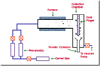
Chemical Vapour Deposition (CVD) refers to the formation of a non-volatile solid film of nano dimension on a substrate from the reaction of vapour phase chemical reactants containing the right constituents. A reaction chamber is used for this process, into which the reactant gases are introduced to decompose and react with the substrate to form the film of nano dimension. Chemical vapour deposition is used in a multitude of semiconductor wafer fabrication processes, including the production of amorphous and polycrystalline thin films (such as polycrystalline silicon), deposition of SiO2 (CVD SiO2) and silicon nitride, and growing of single-crystal silicon epitaxial layers. A typical CVD system consists of the following parts: 1) Sources of and feed lines for gases; 2) Mass flow controllers for metering the gases into the system; 3) A reaction chamber or reactor; 4) A system for heating up the wafer on which the film is to be deposited; and 5) Temperature sensors.
Figure 11
In this technique, the precursor vapour is passed through a hot walled reactor. The precursor decomposes and nanoparticles nucleate in the gas phase. The nanoparticles are carried by the gas stream and collected on a cold finger. The size of the nanoparticles is determined by the particle residence time, temperature of the chamber, precursor composition, and pressure. A basic CVD process consists of the following steps: 1) A predefined mix of reactant gases and diluents inert gases are introduced at a specified flow rate into the reaction chamber; 2) The gas species move to the substrate; 3) The reactants get adsorbed on the surface of the substrate; 4) The reactants undergo chemical reactions with the substrate to form the film; and 5) The gaseous by-products of the reactions are desorbed and evacuated from the reaction chamber. During the process of chemical vapour deposition, the reactant gases not only react with the substrate material at the wafer surface (or very close to it) but also in the gas phase in the reactor's atmosphere. Reactions that take place at the substrate surface are known as heterogeneous reactions and are selectively occurring on the heated surface of the wafer where they create good-quality films of nano dimension. Reactions that take place in the gas phase are known as homogeneous reactions. Homogeneous reactions from gas-phase aggregates of the depositing material, which adhere to the surface poorly and at the same time form low-density films with lots of defects. In short, heterogeneous reactions are much more desirable than homogeneous reactions during chemical vapour deposition. |
|
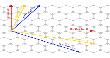
| (n,0) zigzag nanotube
|
| (n, n) armchair nanotube
|
| (n, m) chiral nanotube
|
|
|
|
In the past two decades, hundreds of novel NSMs (nanostructured materials) have been obtained therefore, the need for their classification becomes important. NSMs as a subject of nanotechnology are low dimensional materials comprising of building units of a submicron or nanoscale size at least in one direction, and exhibiting size effects. The first classification idea of NSMs was given by Gleiter in 1995, and further was explained by Skorokhod in 2000. However, Gleiter and Skorokhod scheme was not fully considered because 0D, 1D, 2D, and 3D structures such as fullerenes, nanotubes, and nanoflowers were not taken into account. After that, Pokropivny, and Skorokhod reported a modified classification scheme for NSMs, in which 0D, 1D, 2D, and 3D NSMs are included.
0D Nanostructured Materials In the past 10 years, significant progress has been made in the field of 0D NSMs. 0D NSMs such as uniform particle arrays (quantum dots), heterogeneous particle arrays, core-shell quantum dots, onions, hollow spheres, and nano lenses have been synthesized by several research groups. 0D NSMs, such as quantum dots have been extensively studied in light-emitting diodes (LEDs), solar cells, single-electron transistors, and lasers. A 0D structure is the simplest block that can be used for the design of nanomaterials. In this case, the three dimensions are in the nanometre regime and have a diameter of less than 100 nm. Nanoparticles, nanocrystals, and nanoclusters correspond to this group. Nanoparticles They are nanostructures usually used to define all 0D nanostructures or those that are amorphous and have an irregular shape. So, the nanoparticles can be of natural origin, semiconductor, metal, oxides, fullerenes, or quantum dots.
During manufacturing, the nanoparticles that make up the nanomaterials can be of different sizes, which can vary by more than 15%, and still form the nanomaterial without affecting its design. 3D nanomaterials should not be included in the category of nanostructures unless their internal structure is nanostructured. Nanoclusters As well as the nanoparticles, they have an irregular structure besides being semi-crystalline, but they are tinier than the nanoparticles. Its diameter ranges between 1, and 10 nm. Also, nanoclusters are sensitive to their size and become more reactive if they increase or decrease proportionally. Nanocrystals They are monocrystalline nanostructures, whose size ranges from 1 to 30 nm. Semiconductor nanocrystals are more commonly known as quantum dots.
In the last decade, 1D NSMs have stimulated an increasing interest due to their importance in research, and developments, and have a wide range of potential applications. It is generally accepted that 1D NSMs are ideal systems for exploring a large number of novel phenomena at the nanoscale and investigating the size, and dimensionality dependence of functional properties. They are also expected to play an important role as both interconnects, and the key units in fabricating electronic, optoelectronic, and EEDs with nanoscale dimensions. The field of 1D NSMs such as nanotubes has attained significant attention. 1D NSMs have a profound impact on nanoelectronics, nanodevices, and systems, nanocomposite materials, alternative energy resources, and national security. We show the 1D NSMs, such as nanowires, nanorods, nanotubes, nanobelts, nanoribbons, and hierarchical nanostructures, which have been synthesized in the laboratories. They have a variable length, conserving two dimensions (height, and width) in the nanometer regime; to these correspond the nanowires and nanotubes. Nanowires They are elongated crystalline structures whose characteristics stand out for their conductive or semiconducting properties. Nanowires have been obtained from various metallic materials, semiconductors, oxides, etc. In recent years, nanowires have shown special scientific interest due to their potential applications in nanoelectronics, optoelectronics, and sensors. Nanotubes They are tubular structures with a hollow interior. There are nanotubes synthesized, and characterized by inorganic laminar materials. However, the most studied are carbon nanotubes (CNT's).
Two-dimensional nanomaterials (2D) 2D nanostructures have two dimensions outside of the nanometric size range. In recent years, a synthesis of 2D NSMs has become a focal area in materials research, owing to their many low dimensional characteristics different from the bulk properties. In the search for 2D NSMs, considerable research attention has been focused over the past few years on the development of 2D NSMs. 2DNSMs with certain geometries exhibit unique shape-dependent characteristics and subsequent utilization as building blocks for the key components of nanodevices. Besides, a 2D NSMs are particularly interesting not only for a basic understanding of the mechanism of nanostructure growth, but also for investigation, and developing novel applications in sensors, photocatalysts, nano-containers, nanoreactors, and templates for 2D structures of other materials. There are 2D NSMs such as junctions (continuous islands), branched structures, nano-prisms, nanoplates, nanosheets, nanowalls, and nanodisks. They are nanomaterials formed by very thin layers; thin nanolayers with areas of undefined size, and a thickness between 1, and 100 nm. Graphene is the most notable example because, due to its multiple, and exceptional properties, it has the potential to revolutionize technology. Its possible applications extend to very diverse areas, ranging from the miniaturization of electronic devices to the elaboration of drugs against cancer in medicine. |
|
Sputtering Sputtering is a physical process in which atoms in a solid-state (target) are released and pass into the gas phase by bombardment with energetic ions (mainly noble gas ions). Sputtering is usually understood as the sputter deposition, a high vacuum-based coating technique belonging to the group of PVD processes. Sputtering is used as a cleaning method for the preparation of high-purity surfaces and it is also used for analyzing the chemical composition of surfaces. Sputtering is a mechanism by which atoms are dislodged from the surface of a material as a result of a collision with high-energy particles. Thus, PVD by Sputtering is a term used to refer to a physical vapor deposition (PVD) technique wherein atoms or molecules are ejected from a target material by high-energy particle bombardment so that the ejected atoms or molecules can condense on a substrate as a thin film nano dimension. Sputtering has become one of the most widely used techniques for depositing various metallic films on wafers, including aluminum, aluminum alloys, platinum, gold, TiW, and tungsten. Process of Sputtering The principle of Sputtering is to use the energy of plasma (partially ionized gas) on the surface of a target (cathode), to pull the atoms of the material one by one and deposit them on the substrate. Sputtering as a deposition technique may be described as a sequence of these steps: 1) Ions are generated and directed at a target material; 2) The ions sputter atoms from the target; 3) The sputtered atoms get transported to the substrate through a region of reduced pressure; and 4) The sputtered atoms condense on the substrate, forming a thin film. To do this, plasma is created by the ionization of pure gas. Usually, we take Argon gas. Ionization of a pure gas is done by applying potential difference (pulsed DC), or by electromagnetic excitation. Thus plasma is composed of Ar+ ions which are accelerated and confined around the target due to the presence of a magnetic field. Each ionized atom strikes the target and transfers its energy and rips an atom, having enough energy to be projected to the substrate.
Figure 7
The plasma is created at relatively high pressures (10-1 - 10-3 mbar), but it is necessary to start from a lower pressure before the introduction of Argon, to avoid contamination due to the residual gases. The diversity of sputtering target shapes (circular, rectangular, Delta, tubular...) and the materials used allows creating all types of thin layers, including alloys during a single run. Basics of the Sputtering Process When bombarding a surface with ions, various effects may occur, depending on the ions used and their kinetic energy: 1. Material is removed from the bombarded target (cathode). This is the sputtering described here. 2. The ions are incorporated into the target material and enter there, possibly a chemical compound. This effect is then called (reactive) ion implantation. 3. The ions condense on the bombarded substrate, where they form a layer: ion beam deposition. If a material removal is intended, the ions must have a certain minimum energy. The impinging ion transmits its impulse to atoms of the bombarded material (target), which then - similar to the billiards - trigger further collisions. After several collisions, some of the target atoms have a momentum away from the target interior. If such an atom is sufficiently close to the surface and has sufficiently high energy, it leaves the target. The sputter yield depends
To eject an atom from the target, the ions must have material-dependent minimum energy (typically 30-50 eV). Above this threshold, the yield increases. However, initially, it increases strongly then flattens rapidly. At high ion energies, this energy is deposited even deeper into the target and thus barely reaches the surface. The ratio of the masses of ion and target atom determines the possible momentum transfer. For light target atoms, maximum yield is achieved when the mass of target and ion approximately match. However, as the mass of the target atoms increases, the maximum of the yield shifts to ever higher mass ratios between the ion and the target atom. The ion bombardment generates not only neutral atoms, but also secondary electrons and, to a lesser extent, secondary ions and clusters of different masses. The energy distribution of the dissolved atoms has a maximum at half the surface binding energy but falls to high energies only slowly so that the average energy is often an order of magnitude above. This effect is exploited in analysis methods of surface physics and thin-film technology as well as for the production of thin layers (sputter deposition). Advantages 1) Sputtering can be achieved from large-size targets, simplifying the deposition of a thin film with uniform thickness over large wafers; 2) Film thickness is easily controlled by fixing the operating parameters and simply adjusting the deposition time; 3) Control of the alloy composition, as well as other film properties such as step coverage and grain structure, is more easily accomplished than by deposition through evaporation; 4) Sputter-cleaning of the substrate in a vacuum before film deposition can be done; 5) Device damage from X-rays generated by electron beam evaporation is avoided. Disadvantages 1) High capital expenses are required; 2) The rates of deposition of some materials (such as SiO2) are relatively low; 3) Some materials such as organic solids are easily degraded by ionic bombardment; 4) Sputtering has a greater tendency to introduce impurities in the substrate than deposition by evaporation because the former operates under a lesser vacuum range than the latter. |
SOL-GEL PROCESS Sol-gel is a low temperature, highly controllable, and cost-effective method for the production of homogeneous, highly stoichiometric, and high-quality ultrafine nanostructures. The sol-gel process involves the formation of a colloidal suspension of particles called “sol", and the transition of the colloidal “sol" into a solid called the "gel" phase. The sol-gel process allows the fabrication of thin films with a large variety of properties. Sol-gel chemistry is a remarkably versatile approach for fabricating materials. The sol is made of solid particles of a diameter of a few hundred nm, usually, inorganic metal salts, suspended in a liquid phase. In a typical sol-gel process, the precursor is subjected to a series of hydrolysis, and polymerization reactions to form a colloidal suspension, and then the particles condense in a new phase, the gel, in which a solid macromolecule is immersed in a solvent. Sol is obtained by either hydrolysis or polymerization reactions by adding suitable reagents in the precursor solution. The sol can be deposited onto preferred substrates as thin films using two techniques, (1) spin coating (2) dip coating The gelation process done through condensation of the sol or the addition of polymers converts this sol to gel. This gel can be used to form materials of different types such as nanoparticles, xerogel, glass, or ceramics depending upon the further processing steps involved.
Figure 8: Schematic diagram of sol-gel processing. Nanoparticles and xerogels can be obtained by simple evaporation of the solvent. The obtained xerogel can be formed as ceramics by heat treatment, and glassy nature can be induced by melting techniques. Thus, the sol-gel method can be used to obtain different forms of materials, controlled phase, and shape, and size of the derived materials The parameters that could be controlled in the sol-gel method includes (1) Concentration of precursor used, (2) Nature of solvent used, (3) the pH of the solution, (4) Type of additives added, and their concentration, (5) Pre, and post-heat treatment of the materials, (6) Aging of the solution, and (7) Nature of polymer used for condensation The particles formed in the gel matrix possess uniform shape, and size that enhances the optical, electrical, magnetic, and other intrinsic nature of the materials. Of the factors listed above, pH, nature, and concentration of catalyst, and temperature have been identified as most important. Thus, by controlling these factors, it is possible to vary the structure and properties of the sol-gel-derived inorganic network over wide ranges. The solutions exhibit a strong concentration dependence on the intrinsic viscosity, and a power-law dependence of the reduced viscosity. The sol solution is deposited on the substrates by spraying, dipping, or spinning |
|
|
Chemical Vapour Deposition (CVD) refers to the formation of a non-volatile solid film of nano dimension on a substrate from the reaction of vapour phase chemical reactants containing the right constituents. A reaction chamber is used for this process, into which the reactant gases are introduced to decompose and react with the substrate to form the film of nano dimension. Chemical vapour deposition is used in a multitude of semiconductor wafer fabrication processes, including the production of amorphous and polycrystalline thin films (such as polycrystalline silicon), deposition of SiO2 (CVD SiO2) and silicon nitride, and growing of single-crystal silicon epitaxial layers. A typical CVD system consists of the following parts: 1) Sources of and feed lines for gases; 2) Mass flow controllers for metering the gases into the system; 3) A reaction chamber or reactor; 4) A system for heating up the wafer on which the film is to be deposited; and 5) Temperature sensors.
Figure 11
In this technique, the precursor vapour is passed through a hot walled reactor. The precursor decomposes and nanoparticles nucleate in the gas phase. The nanoparticles are carried by the gas stream and collected on a cold finger. The size of the nanoparticles is determined by the particle residence time, temperature of the chamber, precursor composition, and pressure. A basic CVD process consists of the following steps: 1) A predefined mix of reactant gases and diluents inert gases are introduced at a specified flow rate into the reaction chamber; 2) The gas species move to the substrate; 3) The reactants get adsorbed on the surface of the substrate; 4) The reactants undergo chemical reactions with the substrate to form the film; and 5) The gaseous by-products of the reactions are desorbed and evacuated from the reaction chamber. During the process of chemical vapour deposition, the reactant gases not only react with the substrate material at the wafer surface (or very close to it) but also in the gas phase in the reactor's atmosphere. Reactions that take place at the substrate surface are known as heterogeneous reactions and are selectively occurring on the heated surface of the wafer where they create good-quality films of nano dimension. Reactions that take place in the gas phase are known as homogeneous reactions. Homogeneous reactions from gas-phase aggregates of the depositing material, which adhere to the surface poorly and at the same time form low-density films with lots of defects. In short, heterogeneous reactions are much more desirable than homogeneous reactions during chemical vapour deposition. |
|
| (n,0) zigzag nanotube
|
| (n, n) armchair nanotube
|
| (n, m) chiral nanotube
|
