Unit 05
Nano material
Q-1What are nano material?
The designing and making up of anything whose use depends on the specific structure at nanoscale. These possess the different properties at reducing scale. The measurement can be taken in notice at 100 nanometers and lesser is called as the nanotechnology. This includes the materials made by the manipulation of up of atoms or molecules. They are composed up of metals, ceramics, polymers, organic materials in simpler way these all are made up of carbon compounds. The technology that we deal with in taking the consideration up of the Nano material is called as the nanotechnology.
Q-2Enlist the different sources of nano material.
Nano materials are found basically form following three sources:
1) Engineered
2) Incidental
3) Natural
Q-3Explain the structure of fullerene and its applications.
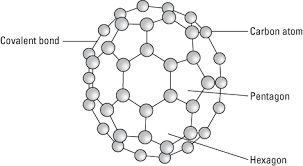
Fullerene is a soccer ball like structure which is hollow from inside and is polymorphic in nature (arrange in hexagon and pentagon form) These are arranged in manner that possess 2 hexagons share a common wall while 2 different pentagons never share the common wall. Each carbon atom is sp2 hybridized. Electric spark is produced at graphite ectrode at inert atmosphere and low pressure which gives back black soot that consist of fullerene and impurities. These impurities are removed by the method of sublimation.

Properties:
All carbon atoms are sp2 hybridized with FCC in nature. This is mustard yellow in color. The fullerene may be Exohederal or Endohederal structure based on the occupying the space.
Applications:
1-Used as super conductors
2-Fulleren is used in making the Ferro magnets
3-It can be used for making non-linear electronic devices.
Q-4What are nano tubes?
Carbon nano tubes (CNTs) are cylindrical molecules that consist of rolled-up sheets of single-layer carbon atoms. They can be single-walled with a diameter of less than 1 nm or multi-walled, consisting of several concentrically interlinked nano tubes, with diameters reaching more than 100 nm. Their length can reach several micrometers or even millimeters.
Q-5What are nano wires?
Nanowires are cylindrical solid wires structures with one of the dimensions smaller than 100 nm and length few micrometers. Nanowires are quantum mechanically one-dimensional structures when their diameter is comparable to the electron’s de Broglie wavelength in the plane perpendicular to the growth direction. One dimensional confinement of electrons in nano wires causes the change in density of states and allowed energy levels in nano wires. Quantum confinement in nano wires also allows the study of other unique phenomena such as ballistic transport, coulomb blockade and phonon confinement. One interesting phenomenon observed in nano wires is that the band gap is altered according to requirement which is an important parameter in fabricating devices for specific applications. Since the band gap increases with the decrease of nano wire diameter, nano wire can emit visible light with high efficiency. Nano wire band gap is also affected by the surface chemistry because of the high surface area to volume ratio. Depending on the Passavant on the nano wire surface the band gap can also be increased or decreased accordingly. A well accepted mechanism for the growth of nano wires through gas phase reaction is vapor liquid-solid process. To grow any nano wire, the material used must be soluble in the catalyst nano particles. E.g.: to grow silicon nano wire gold nano particles are used because silicon vapor is soluble in gold nano particles. To grow gallium nitride nano wire iron nano particles are used because the reactants gallium and nitrogen are soluble in iron nano particles.
Q-6Explain top down approach.
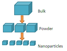
Top down approach deals with the breaking down of bulk material into nano sized particles. Top-down synthesis techniques are extension of those that have been used for producing micron sized particles. Top-down approaches are inherently simpler and depend either on removal or division of bulk material or on miniaturization of bulk fabrication processes to produce the desired structure with appropriate properties. The biggest problem with the top-down approach is the imperfection of surface structure. E.g.: nano wires made by lithography are not smooth and may contain a lot of impurities and structural defects on its surface.

Q-7Explain bottom up approach.
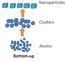
Bottom –up approach refers to the build-up of a material from the bottom: atom-by-atom, molecule-by-molecule or cluster-by-cluster. This route is more often used for preparing most of the nano-scale materials with the ability to generate a uniform size, shape and distribution. It effectively covers chemical synthesis and precisely controlled the reaction to inhibit further particle growth. Although the bottom-up approach is nothing new, it plays an important role in the fabrication and processing of nanostructures and nano materials.

Q-8What are nano electronics?
Nanoelectronics refers to the use of nanotechnology in electronic components. The term covers a diverse set of devices and materials, with the common characteristic that they are so small that inter-atomic interactions and quantum mechanical properties need to be studied extensively. Some of these candidates include: hybrid molecular/semiconductor electronics, one-dimensional nano tubes.
Nano electronic devices have critical dimensions with a size range between 1 nm and 100 nm. Recent silicon MOSFET (metal-oxide-semiconductor field-effect transistor, or MOS transistor) technology generations are already within this regime, including 22 nanometer CMOS (complementary MOS) nodes and succeeding 14 nm, 10 nm and 7 nm Fin FET (fin field-effect transistor) generations. Nano electronics are sometimes considered as disruptive technology because present candidates are significantly different from traditional transistors.
Q-9Enlist the applications of nano material.
1- Nano material will be used as the next generation computer chips.
2- Nano material will be responsible for the High Definition TV.
3- Branch deals in reducing the cost of the flat panel displays.
4- Nanotechnology plays a major role in improving the density of the battery.
5- Nanotechnology contributes in the changing trends by playing the major role in improving the sensivity of the sensors.