Unit-2
Question Bank
Q1) Write difference between Schottky and pn junction diode?
Sol: 
Q2) Explain Clipper with neat circuit diagram ?
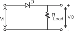
Sol: Series clipper CKT:-
1)Series Negative clipper :- Ideal diode
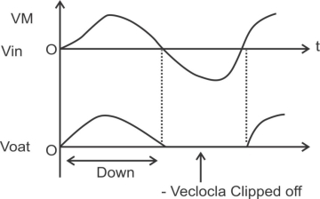
Operation:-
In the positive half cycle of the sinusoidal ilp the diode is forward biased. Being an ideal diode , it acts as a closed switch & connects the load across the ilp the load vtgthere fore equal to the ilpvtg in the positive half cycle.
In the –ve half cycle of the diode is reverse biased acts as an open ckts/w the load vtg is therefore zero during the –ve half cycle.
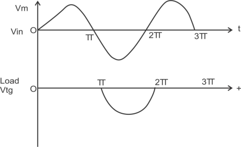
2) Series Positive clipper:-

Series clipper with a D.C supply biased [clippers] :-
1) Biased Series –ve Clipper:-
2)

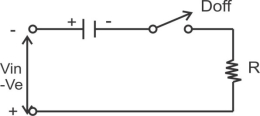
Operation:-
The operation of this ckt can be divided in to there intervals
1) Operation when in is +ve but less than v:-in the positive half cycle of the ilp as long as vin v the diode is not forward biased, therefore from to and then from t2 to t/2 shown in fig below the diode will remain in off state and the o/p voltage will be zero.

Fig -a)Equivalent ckt for +vin>v -
-

Fig b) Equivalent ckt for vin –ve
Q3) A 5.0V stabilized power supply is required to be produced from a 12V DC power supply input source. The maximum power rating PZ of the zener diode is 2W. Using the zener regulator circuit above calculate:
a). The maximum current flowing through the zener diode.
Maximum current = Watts/ Voltage =2W/5V =400mA
b). The minimum value of the series resistor, RS
 = 17.5 Ω
c). The load current IL if a load resistor of 1kΩ is connected across the zener diode.

d). The zener current IZ at full load.
Iz =Is -Il =440mA – 5mA = 395mA
Q4) Explain half wave rectifier?
Sol: Half Wave rectifier
1) Due to the unidirectional current flow through the transformer there is a possibility of core saturation to avoid this transformer size must be increased.
2) Ripple factor is high.
3) Low rectification effecting.
4) Law TUF.
5) Law D.C O/P VTG & current.
6) Large filter component are required.
ADVANTAGES:-
1) Simple Construction.
2) Component required less.
3) Small size.
APPLICATION:-
Walkman, law cost power supply.
Q5) What are varactor diodes?
Sol: The diode whose internal capacitance varies with the reverse voltage are known as varactor diodes. They work only in reverse bias. They are used where variable capacitance is required.

As the diode operates only in reverse bias the width of depletion region increases and hence the current decreases. It is used as a charge storing device.
The transition capacitanceCT = 
In reverse bias the width of depletion region increases and hence the capacitance decreases. The VI characteristics shows the same

Q6) Explain tunneling effect in tunnel diode?
Sol: It is a heavily doped p-n junction diode in which the electric current flows due to tunnelling. The germanium metal is used in tunnel diode. As they are heavily doped with impurities, they are negative resistance device. The current across the diode decrease with increase in voltage.
Tunnelling Effect:
This means penetration of electrons from small depletion region from n-side conduction band to p-side valence band. The width of depletion region depends on the impurities added less the number of impurities added wider the depletion region and vice versa.
As the tunnel diodes are heavily doped so they have narrow depletion region. There is built-in potential in this narrow depletion region. This electric field in the depletion region exerts electric force in a direction opposite to that of the external electric field.


In tunnel diode the VB and CB energy in n type are lower than the p type and dure to narrow depletion region the electrons directly tunnel across this small depletion region from n-side CB to p-side VB.
Q7) What is diffusion capacitance?
Sol: In forward biased the potential barrier at the junction decreases. As a result, holes get injected from the P-side to the N-side and electron get injected from the N-side to the P-side. These injected charges get stored near the junction just outside the depletion layer, holes in the N-region and electrons in the P-region. Due to charge storage, the voltage lags behind the current producing the capacitance effect. Such a capacitance is called diffusion capacitance or storage capacitance CD
CD = 
I = 
 = mean life time of hole
Q = stored charge
Tp = 
LP = diffusion length of holes
Dp= Diffusion constant for holes
CD =  =
= 
CD = 
For forward diode CD as well as CT are present but CD>>CT. Hence CT can be neglected
For reverse bias CT>>CD. Hence CD can be neglected.
Q8) Explain diode as a switch?
Sol: Whenever a specified voltage is exceeded, the diode resistance gets increased, making the diode reverse biased and it acts as an open switch. Whenever the voltage applied is below the reference voltage, the diode resistance gets decreased, making the diode forward biased, and it acts as a closed switch.
The following circuit explains the diode acting as a switch.

A switching diode has a PN junction in which P-region is lightly doped and N-region is heavily doped. The above circuit symbolizes that the diode gets ON when positive voltage forward biases the diode and it gets OFF when negative voltage reverse biases the diode.
As the forward current flows till then, with a sudden reverse voltage, the reverse current flows for an instance rather than getting switched OFF immediately. The higher the leakage current, the greater the loss. The flow of reverse current when diode is reverse biased suddenly, may sometimes create few oscillations, called as RINGING.
This ringing condition is a loss and hence should be minimized. To do this, the switching times of the diode should be understood.
Q9) Draw circuit diagram and explain zener diode?
Sol: Zener Diode
- Zener diode is a special type of p-n junction semiconductor diode in this diode the reverse breakdown voltage is adjusted precisely between 3v to 200v.
- Its applications are based on this principle hence Zener diode is called as a breakdown diode.
- The doping level of the imparity added to manufacture the zener diode is controlled in order to adjust the precise value of breakdown voltage.
PRINCIPLE OF OPERATION: - A zener diode can be forward biased or reverses biased. Its operation in the forward biased mode is same as that of a p-n junction diode but its operation in the reverse biased mode is sustainably deferent.


Q10) What are photodiodes explain its working?
Sol: The photodiode is a p-n junction semiconductor diode which is always operated in the reverse biased condition.
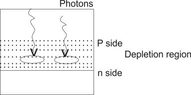
The light is always focused through a glass lens on the junction of the photodiode As the photodiode is reverse biased the depletion region is quite wide, penetrated on both side of the junction.
The photons incident on the depletion region will impact their energy to the Ions present in depletion region and generates e hole pairs.
The photons incident on the depletion region so the number of electron hole pairs will be generated depends on the intensity of light [number of photons] These and holes will be attracted towards the +ve& -ve terminals respectively of the photo current ,
With increase in the light intensity more number of e hole pairs are generated and the photo current increases thus the photocurrent is proportional to the light intensity.