Question Bank
Unit-3
Q1) Determine the values of VCC RC and RB of a fixed bias configuration for a given load line and defined Q point.

Solution:

Q2) Explain input characteristics of CB ?
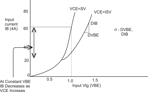
Sol: Input Characteristic: is always a graph of input current verses input vtg. For common base (CB) configuration input current is the emitter current (IE) & I/p vtg. Is the emitter to the base vtg (VEB)
The I/p Characteristic is plotted at a constant O/p vtg. VCB
Q3) What is BJT explain its construction?
Sol: *BJT:-The BJT is constructed with the three draped semiconductors region’s separate by two Pn junctions as shown below
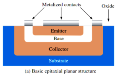
-Basic epitaxial planner structures.
-Three terminal with region’s are called emitter, base and collector.
-The physical representation of the two types of BJT’s,
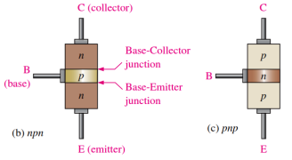
One type consists between two regions separated by a P region (npn) and other type consists of two p regions separated by an n region (pnp).
-The Pn junction joining the base region and the emitter region is called the base emitter junction.
-The Pn junction joining the base region and the collector region is called the base collector junction.
-The base region is lightly doped and very thin compared to the heavily doped emitter and the moderately doped collector regions.
Q4) How do the BJT work?
Sol: Base Transistor Operation:-
In order for the transistor to operate properly as an amplifier the two pn junction must be correctly biased with the external D.C vtg.
-The next figure shows the proper bias arrangement for both the npn and pnp transistors for active operation as an amplifier.
-In both the cases the base emitter
(BE) junction is forward biased & the base collector junction (BC) junction is reverse biased
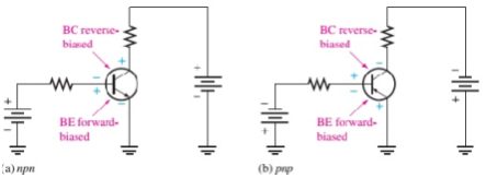
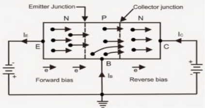
- As from above figure consider n-p-n transistor. The forward bias from base to emitter narrow’s the BE depletion region and the reverse bias from base to collector widens the BC depletion region shown in figure.
- The heavily doped N-TYPE emitter region is full with conduction band(frep) electron’s that easily diffuse through the forward biased BE junction into the p-type base region where they become minority carrier’s same as forward biased diode region
- The base region is lightly doped & very thin so that it has a very limited number of holes.
- Those only a small percentage of all the e-flowing the BE junction can combine with the available holes in the base.
- The relatively few recombined flow out of the base lead as valance electrons, forming as small base current.
- Most of the e flowing from the emitter into the thin lightly dooped base region do not recombine but diffuse into the BC depletion region.
- The BC depletion region diffuse e is being pulled across the reverse biased BC junction by the attraction of the collector supply vtg.
- The electrons now move through the collector region, out through the collector lead into the +ve terminal of the collector vtg source. This forms the collector electrons current.
- The collector current is much larger than the base current.
- This is the reason transistor exhibit current gain.
Q5) Derive the relation for base current and emitter current in CB mode?
Sol:The collector current is IC of the common base configuration is given by
Ic=Ic(INI)+ICBO
-Where the Ic(INI) called the injected collectors current and it is due to the number of electrons crossing the collectors base junction.
-ICBO :- This is the reverse saturation current flowing due to the minority carrier’s between the collector and base when the emitter is open
-ICBO flow’s due to the reverse biased collector’s base junction. As ICBO negligible as compared to Ic(INI) we can neglect it in practice.
.’. Ic=Ic(INI)………………………practically
Ic=ICBO………………with emitter open
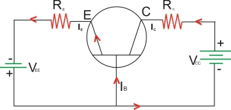
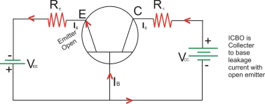
 Emitter is open
 ICBO
ICBO
Collector is to base control
-Since the ICBO flow’s due to terminally generated minority carrier’s it increases with increase the temperature.
-It doubles it’s value for every 100c rise in temperature.
-Current amplification factor or current gain (ddc):-
Current amplification factor or current gain is the ratio of collector current due to the injection to the total emitter current
αd.c = Ic(INI)
-The value of the ddc for CB configuration will always be less than 1.This is because
Ic(INI)<IE.
-Typically the value of d.d.c ranges between 0.95 to 0.995 depending upon the thickness of the base region.
-Larger the thickness of the base region smaller the value of the d.d.c
Ic(INI)=d.d.c.IE
Hence the expression for IC is given by
IC=αd.c IE + ICBo--------------------I
But the ICBo is negligibly small
IC d.d.c IE
* Expression for IB:-
IE=IB+IC
IE=αd.cIE+ICBo+IB…………………from I
IB=(1-αd.c)IE-ICBo
Neglecting ICBo
IB=(1-αd.c)IE
Q6) Explain Eber’s moll model?
Sol: This model of transistor can operate in forward active mode. The circuit has two diodes with two current sources connected as shown below. The diodes represent base-emitter and base collector. The directions of current are as shown in the figure below. The minority carriers flow through the base region.

Fig: Eber’s Moll model for NPN bipolar junction transistor
IE = IF – αR IR
IB = (1- αF) IF + (1- αR) IR
IC = -IR + αF IF
The Eber’s Moll model parameters are related as
IE,sαF = IC,sαR
The above relation is called as reciprocity relation. But for case when there is no minority carrier diffusion due to uniform base doping and equal voltages of base-emitter and base-collector junctions the relation becomes
IF(VBE) αF = IR (VBC+VBE) αR
Where
IF = Forward current of diode
IR = reverse current of diode
αF = Forward transport factor
αR = Reverse transport factor
IE,s = Saturation current of base-emitter diode
IC,s = Saturation current of base-collector diode
Q7) what are the region of operations of BJT?
Sol: 
Q8) Explain output characteristics of CB?
Sol: Output Characteristic is always a graph of O/p current versus O/p Vtg.
For the CB configuration the O/p current is collector current (IC) of the output voltage is collector to base vtg. (VCB)
Output Characteristic is plotted for a constant value of I/p current (IE)
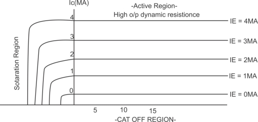
O/p Characteristic of a n-p-n transistor in CB Configuration
Dynamic O/p resistance (ro)
Ro =  / I
/ I  constant
In the active region Ic does not depend on VCB. It depends only on the I/p current IE. That is why the transistor is called as a current controlled or current operated device.
Q9) What is load line in transistor characteristics?
- Sol: The load line solution was found by superimposing the actual characteristics on a plot of network equation involving the same network variables.
- It is known as load line analysis as load of network defined the slope of the straight line connecting the points defined by network parameters.
- The smaller the load resistance, the steeper the slope of the network load line.

Fig.: DC Load Line (Ref. 2)
- The output equation is given by,

- The characteristic curve is drawn as

Fig.: DC Load Line characteristic curve (Ref. 2)
- When Ic = 0mA then

- If we choose VCE = 0V then,

Q10) Draw npn CB transistor?
Sol
: 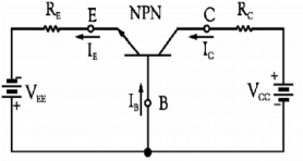
The I/p is applied between the emitter and the base. The base acts as a common terminal between the I/p and o/p.
-The input vtg is therefore VEB and the input current is IE.
-The output is taken between the collector and the base therefore the output vtg is VCB and the output current is IC.