Question Bank
Section B
- Explain star and delta load transformations?
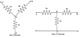
In star connection, the components are connected in such a way that one end of all the resistors or components are connected to a common point.
By the arrangement of three resistors, this star network looks like alphabet Y hence, this network is also called as Wye or Y network.
The equivalent of this star connection can be redrawn as T network as shown in below figure.
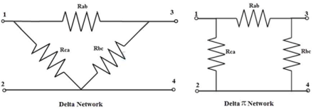
In a delta connection, the end point of each component or coil is connected to the start point of another component or coil.
It is a series connection of three components that are connected to form a triangle. The name indicates that connection look like an alphabet delta (Δ).
The equivalent delta network can be re-drawn, to look like a symbol Pi (or four terminal network) as shown in figure. So, this network can also be referred as Pi network.
Star to delta conversion to final equivalent resistance
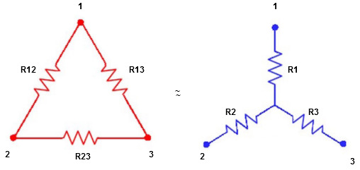
We know that (from delta to star conversion)
R1 =  …….①
…….①
R2 =  …..②
…..②
R1 =  ……③
……③
Multiply ① X ② L.H.S and R.H.S
R1 R2 = …….④ where
Similarly multiply ② X ③
R2 R3 = …….⑤
…….⑤
And ③ X①
R1 R3 = …….⑥
…….⑥
Now add equation ④, ⑤, and ⑥ L.H.S and R.H.S


 ……refer eq. ②
 =
=  +
+  +
+ 
 =
=  +
+ 

(Delta) star star
Similarly R23 = R2+R3 + 
R23 = R1+R2 + 
- Delta to Star Conversion to Find (Req.)
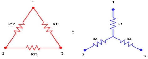
- Equivalent resistance between ① and ②
Delta Star
Star
= R12// (R23 + R13) =R1 + R2
= 
 = R1 + R2
= 

Here let R = R12 + R23 + R13
- Similarly we can find Req. Between 2 and 3
= 
 R2 + R3
- Similarly we can find req. Between 1 and 3

 R1 + R3
Now the 3 equations after equating L.H.S. And R.H.S
R1 + R2 =  …….①
…….①
R2 + R3 =  ……②
……②
R1 + R3 =  …..③
…..③
Now subtract ② and ① on L.H.S. And R.H.S
R2+ R3 – R1 – R2 = 
 R3 – R1 =
  …..④
…..④
Now add equation ④ and ③
R3 – R1 + R1 + R3 = 
2R3 = 

Similarly R1 = 
And R2 = R23 R12/R where R = R12 + R23 + R13
Ie star equivalent from delta network is ratio of product of adjacent branches in delta to the addition of all branches in delta.
2. Explain balanced and unbalanced three- phase circuits?
A 3- phase power system is one with 3 live conductors (e.g. Wires), each carrying AC electricity each shifted by 1/3 cycle from the other two, as shown in the figure below.
This shifting is known as a phase shift, so each live conductor is known as a phase.
If the power being delivered by each phase is equal, then the system is described as balanced; otherwise the system is unbalanced.
If the system is balanced, then the sum of the current through the three phases is 0, so no neutral wire is needed to return the current.
In an unbalanced system the neutral wire acts as a common return for the current from all three phases.
3. Explain measurement of power and power factor?
Power factor, cos(Φ), is an important part of an AC circuit that can also be expressed in terms of circuit impedance or circuit power. Power factor is defined as the ratio of real power (P) to apparent power (S), and is generally expressed as either a decimal value, for example 0.95, or as a percentage: 95%.
Power factor defines the phase angle between the current and voltage waveforms, were I and V are the magnitudes of rms values of the current and voltage.
The mathematical relationship is given as:
Power factor = watts/ volt-amperes
P/S = VI cos ɸ / VI = cos ɸ
Measurement of power
Three Wattmeter method is employed to measure power in a 3 phase, 4 wire system. However, this method can also be employed in a 3 phase, 3 wire delta connected load, where power consumed by each load is required to be determined separately.
The connections for star connected loads for measuring power by three wattmeter method is shown below:
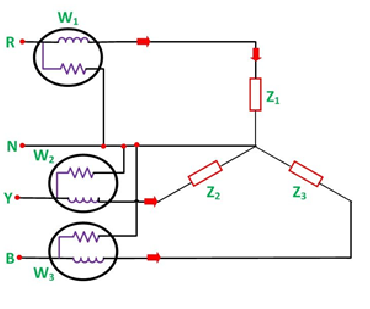
The pressure coil of all the three wattmeters namely W1, W2 and W3 are connected to a common terminal known as the neutral point. The product of the phase current and line voltage represents phase power and is recorded by an individual wattmeter.
The total power in a three-wattmeter method of power measurement is given by the algebraic sum of the readings of three- wattmeter. i.e.
Total power P = W1 + W2 + W3
Where,
W1 = V1I1
W2 = V2I2
W3 = V3I3
Except for 3 phase, 4 wire unbalanced load, 3 phase power can be measured by using only Two Wattmeter Method.
4. What is semiconductor? Explain intrinsic semiconductor?
A semiconductor material is one whose electrical properties lie in between those of insulators and good conductors.
Examples are: germanium and silicon.
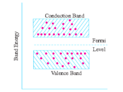
In terms of energy bands, semiconductors can be defined as those materials which have almost an empty conduction band and almost filled valence band with a very narrow energy gap (of the order of 1 eV) separating the two.
Intrinsic semiconductor
An intrinsic semiconductor is one which is made of the semiconductor material in its extremely pure form.
Examples of such semiconductors are: pure germanium and silicon which have forbidden energy gaps of 0.72 eV and 1.1 eV respectively.
The energy gap is so small that even at ordinary room temperature; there are many electrons which possess sufficient energy to jump across the small energy gap between the valence and the conduction bands.
Alternatively, an intrinsic semiconductor may be defined as one in which the number of conduction electrons is equal to the number of holes.
The schematic energy band diagram of an intrinsic semiconductor at room temperature is shown in Fig. Below.
5. Explain N-type and P-type semiconductor ?
Those intrinsic semiconductors to which some suitable impurity or doping agent or doping has been added in extremely small amounts (about 1 part in 108 ) are called extrinsic or impurity semiconductors.
Depending on the type of doping material used, extrinsic semiconductors can be sub-divided into two classes:
(i) N-type semiconductors and
(ii) P-type semiconductors.
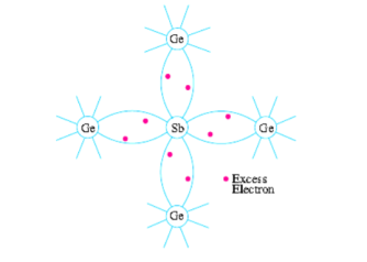
(i) N-type Extrinsic Semiconductor: This type of semiconductor is obtained when a pentavalent material like antimonty (Sb) is added to pure germanium crystal.
As shown in Fig. Below, each antimony atom forms covalent bonds with the surrounding four germanium atoms with the help of four of its five electrons. The fifth electron is superfluous and is loosely bound to the antimony atom. Hence, it can be easily excited from the valence band to the conduction band by the application of electric field or increase in thermal energy.
It is seen from the above description that in N-type semiconductors, electrons are the majority carriers while holes constitute the minority carriers.
P-type Extrinsic Semiconductor:
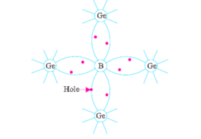
This type of semiconductor is obtained when traces of a trivalent like boron (B) are added to a pure germanium crystal.
In this case, the three valence electrons of boron atom form covalent bonds with four surrounding germanium atoms but one bond is left incomplete and gives rise to a hole as shown in Fig. Below.
Thus, boron which is called an acceptor impurity causes as many positive holes in a germanium crystal as there are boron atoms thereby producing a P-type (P for positive) extrinsic semiconductor. In this type of semiconductor, conduction is by the movement of holes in the valence band.
6. Explain doping effect?
The process of adding an impurity to an intrinsic or pure material is called doping and the impurity is called a dopant. After doping, an intrinsic material becomes an extrinsic material.
When an impurity is added to silicon or germanium without modifying the crystal structure, an N-type material is produced.
In some atoms, electrons have five electrons in their valence band such as arsenic (As) and antimony (Sb). Doping of silicon with either impurity does not change the crystal structure or the bonding process.
The extra electron of impurity atom does not take part in a covalent bonding. These electrons are loosely held together by their originator atoms. The following figure shows alteration of silicon crystal with the addition of an impurity atom.
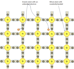
Effect of Doping on N-type Material
The effect of doping on an N-type material is as follows −
- On addition of Arsenic to pure Silicon, the crystal becomes an N-type material.
- Arsenic atom has additional electrons or negative charges that do not take part in the process of covalent bonding.
- These impurities give up or donate, one electron to the crystal and they are referred to as donor impurities.
- An N-type material has extra or free electrons than an intrinsic material.
- An N-type material is not negatively charged. Actually all of its atoms are all electrically neutral.
- These extra electrons do not take part in the covalent bonding process. They are free to move about through the crystal structure.
- An N-type extrinsic silicon crystal will go into conduction with only 0.005eV of energy applied.
- Only 0.7eV is required to move electrons of intrinsic crystal from the valence band into the conduction band.
Normally, electrons are considered to be the majority current carriers in this type of crystal and holes are the minority current carriers. The quantity of donor material added to Silicon finds out the number of majority current carriers in its structure.
The number of electrons in an N-type silicon is many times greater than the electron-hole pairs of intrinsic silicon. At room temperature, there is a firm difference in the electrical conductivity of this material. There are abundant current carriers to take part in the current flow. The flow of current is achieved mostly by electrons in this type of material. Therefore, an extrinsic material becomes a good electrical conductor.
Effect of Doping on P-type Material
The effect of doping on a P-type material is as follows −
- When Indium (In) or Gallium (Ga) is added to pure silicon, a P-type material is formed.
- This type of dopant material has three valence electrons. They are eagerly looking for a fourth electron.
- In P type material, each hole can be filled with an electron. To fill this hole area, very less energy is required by electrons from the neighboring covalent bonded groups.
- Silicon is typically doped with doping material in the range of 1 to 106. This means that P material will have much more holes than the electron-hole pairs of pure silicon.
- At room temperature, there is a very determined characteristic difference in the electrical conductivity of this material.
The following figure shows how the crystal structure of Silicon is altered when doped with an acceptor element — in this case, Indium. A piece of P material is not positively charged. Its atoms are primarily all electrically neutral.
There are, however, holes in the covalent structure of many atom groups. When an electron moves in and fills a hole, the hole becomes void. A new hole is created in the bonded group where the electron left. Hole movement in effect is the result of electron movement. A P-type material will go into conduction with only 0.05 eV of energy applied.
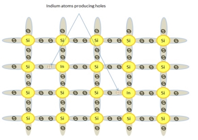
The above figure shows how a P-type crystal will respond when connected to a voltage source. There are larger numbers of holes than electrons. With voltage applied, the electrons are attracted to the positive battery terminal.
7. Explain Fermii levels?
Fermi level is the highest energy state occupied by electrons in a material at absolute zero temperature. As the temperature is increased, electrons start to exist in higher energy states too.
In a p- type semiconductor, there is an increase in the Density of unfilled States.Thus, more electrons can be accommodated at lower energy states.
In a n type semiconductor, the DOS is increased. Thus, electrons are accommodated at higher energy levels.
Fermi level is also defined as the work done to add an electron to the system. More positive (more holes) in a p type semiconductor, mean lesser work needs to be done. Hence a lower Fermi level.
8. Explain charge flow in semiconductors?
When an electric field is applied to a metal, negatively charged electrons are accelerated and carry the resulting current. In a semiconductor the charge is not carried exclusively by electrons. Positively charged holes also carry charge. These may be viewed either as vacancies in the otherwise filled valence band, or equivalently as positively charged particles.
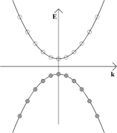
Since the Fermi-Dirac distribution is a step function at absolute zero, pure semiconductors will have all the states in the valence bands filled with electrons and will be insulators at absolute zero. This is depicted in the E-k diagram below; shaded circles represent filled momentum states and empty circles unfilled momentum states. In this diagram k, rather than k, has been used to denote that the wave vector is actually a vector, i.e., a tensor of the first rank, rather than a scalar.
If the band gap is sufficiently small and the temperature is increased from absolute zero, some electrons may be thermally excited into the conduction band, creating an electron-hole pair. This is as a result of the smearing out of the Fermi-Dirac distribution at finite temperature. An electron may also move into the conduction band from the valence band if it absorbs a photon that corresponds to the energy difference between a filled state and an unfilled state. Any such photon must have an energy that is greater than or equal to the band gap between the valence band and the conduction band, as in the diagram below.
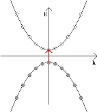
Whether thermally or photonically induced, the result is an electron in the conduction band and a vacant state in the valence band.
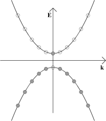
If an electric field is now applied to the material, all of the electrons in the solid will feel a force from the electric field. However, because no two electrons can be in the exact same quantum state, an electron cannot gain any momentum from the electric field unless there is a vacant momentum state adjacent to the state being occupied by the electron.
In the above schematic, the electron in the conduction band can gain momentum from the electric field, as can an electron adjacent to the vacant state left behind in the valence band. In the diagram below, both of these electrons are shown moving to the right.
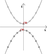
The result of this is that the electrons have some net momentum, and so there is an overall movement of charge. This slight imbalance of positive and negative momentum can be seen in the diagram below, and it gives rise to an electric current.

The vacant site in the valence band which has moved to the left can be viewed as being a particle which carries positive electric charge of equal magnitude to the electron charge. This is therefore a hole.
These schematics are in momentum space. As such, holes should not be thought of as moving through the semiconductor like dislocations when metals are plastically deformed – it suffices to view them simply as particles which carry positive charge.
9. Explain the applications of semiconductor?
- They are used in the designing of logic gates and digital circuits.
- These are used in microprocessors.
- They are also used in analog circuits such as oscillators and amplifiers.
- Used in high voltage applications.
10. Mention the advantages of three phase ac circuits ?
- The conductor material required to transmit the same amount of power over same distance is less.
- Three phase motors are self-starting.
- Torque developed by three phase motor is more uniform.
- Parallel operation of 3-phase ac generators is smooth.
- In case of 3 phase supply, two different voltage can be obtained.
- For given capacity, the frame size of 3 phase motors is small.
- The cost of 3phase machine is low.