Question Bank
Section -C
- Explain PN junction diode?

The left side material is a p-type semiconductor having –ve acceptor ions and +vely charged holes.
The right side material is n-type semiconductor having +ve donor ions and free electrons.
Suppose the two pieces are suitably treated to form pn junction, then there is a tendency for the free electrons from n-type to diffuse over to the p-side and holes from p-type to the n-side . This process is called diffusion.
As the free electrons move across the junction from n-type to p-type, +ve donor ions are uncovered. Hence a +ve charge is built on the n-side of the junction.
At the same time, the free electrons cross the junction and uncover the –ve acceptor ions by filling in the holes.
Therefore a net –ve charge is established on p-side of the junction.
When a sufficient number of donor and acceptor ions is uncovered further diffusion is prevented.
Thus a barrier is set up against further movement of charge carriers. This is called potential barrier or junction barrier Vo. The potential barrier is of the order of 0.1 to 0.3V.
2. Explain depletion layer?
When the P and N-type semiconductor material are placed together, the gradient of large density charge carriers is created on both the P and N side region. The free electrons from N-side cross the region and start combining with the holes, leaving behind the immobile positive donor ions. Similarly, the holes of the P-region combine with the electrons of the N-region and leaving behind the negative acceptor ions.
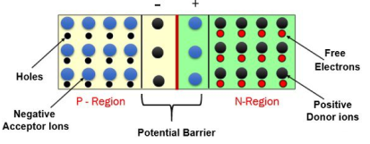
The process is continued until the P and N-region have enough charge carrier for opposing the electrons and holes respectively. The immobile ions (negative acceptor ions and positive donor ions) are concentrated between the N and P-region and create the electric field which acts as a barrier between the flows of charges.
The region is created because of the depleted ions, and hence it is called the depletion region.
3. What is barrier potential ?
The potential barrier in the PN junction diode is the barrier in which the charge requires additional force for crossing the region. In other words, the barrier in which the charge carrier stopped by the obstructive force is known as the potential barrier.
4. Explain the volt-ampere characteristics?
Volt- Ampere characteristics (V-I) of a PN junction diode:
1. Forward Bias - The voltage potential is connected positive, (+ve) to the P-type material and negative, (-ve) to the N-type material across the diode which has the effect of Decreasing the PN-junction width.
2. Reverse Bias - The voltage potential is connected negative, (-ve) to the P-type material and positive, (+ve) to the N-type material across the diode which has the effect of Increasing the PN-junction width.
Forward Characteristics:
Case 1: When the applied forward voltage VF <Vγ, the width of the depletion layer is increased and no current flows through the circuit.
Case 2: When the applied forward voltage VF >Vγ, the charge carriers move towards the junction from P to N and from N to P, due to this the width of the junction gets reduced and at one particular voltage the junction gets damaged ,and forward resistance(RF) offered by the diode will be very less (ideally 0) due to this there will be a flow of current due to majority charge carriers. The current is said to be forward current (IF) which is large.

This condition represents the low resistance path through the PN junction allowing large currents to flow through the diode with only a small increase in bias voltage. The actual potential difference across the junction or diode is kept constant by the action of the depletion layer at approximately 0.3v for germanium and approximately 0.7v for silicon junction diodes. Since the diode can conduct "infinite" current above this knee point as it effectively becomes a short circuit, therefore resistors are used in series with the diode to limit its current flow
Reverse biased PN junction
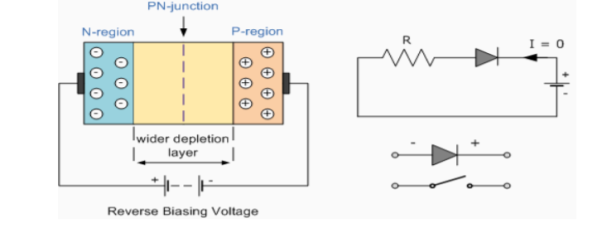
When a diode is connected in a Reverse Bias condition, a positive voltage is applied to the N-type material and a negative voltage is applied to the P-type material. The positive voltage applied to the N-type material attracts electrons towards the positive electrode and away from the junction, while the holes in the P-type end are also attracted away from the junction towards the negative electrode. The net result is that the depletion layer grows wider due to a lack of electrons and holes and presents a high impedance path, almost an insulator.
The result is that a high potential barrier is created thus preventing current from flowing through the semiconductor material.
Reverse Biased Junction Diode showing an Increase in the Depletion Layer This condition represents a high resistance value to the PN junction and practically zero current flows through the junction diode with an increase in bias voltage. However, a very small leakage current (IS) does flow through the junction which can be measured in microamperes, (μA). One final point, if the reverse bias voltage Vr applied to the diode is increased to a sufficiently high enough value, it will cause the PN junction to overheat and fail due to the avalanche effect around the junction. This may cause the diode to become shorted and will result in the flow of maximum circuit current and this shown as a step downward slope in the reverse static characteristics curve below.
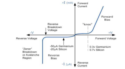
V-I characteristics of PN junction diode
5. What are the current components?
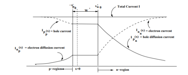
In forward bias there is injected minority carriers on either side of the junction. The holes in n-side and electrons in p-side.
Under low level injection conditions current will be minority currents due to diffusion hence minority drift currents can be neglected.
The injected minority current that is holes since the semiconductor was n-type given by
Ip(x) = AqDp/ Lp {p(0) – po} e -x/Lp
In the above equation p(0) represents the hole concentration at the origin that is the left most part of the semiconductor.
The modified equation is given by two semiconductors (p and n) .Therefore we get
Ipn(x) = AqDp/Lp{ p(xno) – pno} e -x/Lp …………………….(1)
Where Ipn(x) represents the injected minority hole current present in n-side when no bias is applied.
When no bias is applied the depletion region is W = xno + xpo. Thus the n-type specimen starts from xno. Pno represents the hole concentration in n-side under thermal equilibrium .
The injected minority electron current present in p-side becomes
Inp (x) = -AqDn/Ln {n(-xpo) – npo} e-x/Ln ……………………(2)
Hence when bias is applied the penetration of the depletion region on either side is un-symmetrical . The depletion region penetrates more into the lightly doped than heavily doped region. It penetrates more on n-side than p-side.
Let W’ = x’no + x’po be the depletion region afetr bias is applied.
Ipn(x) = AqDp/Lp { p(x’no) -pno} e -x/Lp
Inp(x) = -AqDn/Ln{ n(-x’po)-npo} e-x/ Ln
6. What is transition capacitance?
Transition capacitance:
With the increase of magnitude of reverse bias, majority carriers move away from the junction that is the width W of the depletion layer increases. These uncovered immobile charge on the two sides of the junction constitute a capacitor of incremental capacitance CT given by,
CT = |dQ/dV|………………………….(1)
Where dQ is the increase in the charge resulting from an increase dV in voltage.
Hence, a voltage change dV in the time interval dt will result in a current i given by,
i = dQ/dt = CT dV/dt ----------------------------(2)
This capacitance CT is called the transition capacitance or space charge capacitance or barrier capacitance or depletion layer capacitance.
7. What is diffusion capacitance?
Diffusion capacitance is caused by minority carriers diffusion. When PN diode or bipolar transistor is forward biased, conduction mechanism is mainly due to minority carrier diffusion. Since minority carriers are injected into neutral regions for conduction, these carriers must be removed completely to turn off the diode or the transistor. Injecting and removing these carriers is equivalent to charging and discharging a capacitor.
8. Explain junction diode switching time?
Switching Time of a diode is the time it takes to switch the diode between two states (ON and OFF states)
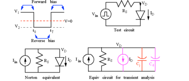
Switching Time of a Diode
• For Forward Bias:
• Current source
ID = IS (e VD/ɸT – 1 )
• C j represents the space-charge ( junction capacitance ).
• C d represents the excess minority carrier charge ( diffusion capacitance ).
o (Note that both of these are small-signal capacitances; to be applicable largesignal analysis, average capacitance values must be used).
• For Reverse bias:
o Eliminate the current source ID and the diffusion capacitance C d.
• Transient response requires finding a solution to:
Iin = ID(t) + (Cd + Cj) d VD(t)/dt
I in = IS (e VD(t) ɸ(t) – 1) + ( Cd + Cj) d VD(t)/dt
9. What is Zener diode?
- Zener diode is a special type of p-n junction semiconductor diode in this diode the reverse breakdown voltage is adjusted precisely between 3v to 200v.
- Its applications are based on this principle hence zenor diode is called as a breakdown diode.
- The doping level of the imparity added to manufacture the zener diode is controlled in order to adjust the precise value of breakdown voltage.
PRINCIPLE OF OPERATION:- A zener diode can be forward biased or reverses biased. Its operation in the forward biased mode is same as that of a p-n junction diode but its operation in the reverse biased mode is sustainably deferent.

10. What is LED?
An LED emits light when electrical energy is applied to it. For proper operation it is necessary to forward bias the LED.
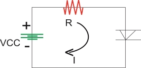
Construction of LED :-
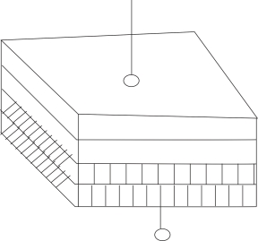
To make emission of light in one direction cup type construction is used for LED.
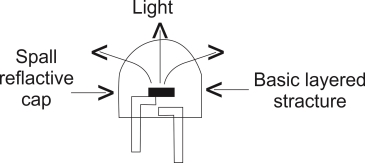
PRINCIPLE LED OPERATION
When the led is forward is forward biased the electrons in the n-region will cross the junction and recombine with the holes in the p- type material.
These free e- reside in the conduction band & hence at a higher energy level than the holes in the valence band
When recombination takes place this e- return peak to the valence band which is at a lower energy level than the conduction band.
While returning back the recombining e-give away the excess energy in the form of light . This process is called as electroluminescence. In this way an LED emits light.
Color of the Emitted Light
Material UseColor ofEmitted Light
i)Gallium Arsenide (GOAS) In fared (IR)
Ii) GaASP(gallium arsenide Red or Yellow
phosphide)
Iii) Gallium phosphide (GAP) Red or Green
Application
Used in 7 Segment Display
11. What is a Photodiode?
The photodiode is a p-n junction semiconductor diode which is always operated in the reverse biased condition.
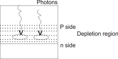
The light is always focused through a glass lens on the junction of the photodiode As the photodiode is reverse biased the depletion region is quite wide, penetrated on both side of the junction.
The photons incident on the depletion region will impact their energy to the Ions present in depletion region and generates e hole pairs.
The photons incident on the depletion region so the number of electron hole pairs will be generated depends on the intensity of light [number of photons] These and holes will be attracted towards the +ve& -ve terminals respectively of the photo current ,
With increase in the light intensity more number of e hole pairs are generated and the photo current increases thus the photocurrent is proportional to the light intensity.
12. Explain varactor diode?
The Varactor diode is made of n-type and p-type semiconductor material. In an n-type semiconductor material, the electrons are the majority charge carrier and in p-type material, the holes are the majority carriers. When the p-type and n-type semiconductor material are joined together, the p-n junction is formed, and the depletion region is created at the PN-junction. The positive and negative ions make the depletion region. This region blocks the current to enter from the PN-region.

The varactor diode operates only in reverse bias. Because of reverse bias, the current does not flow. If the diode is connected in forward biasing the current starts flowing through the diode and their depletion region become decreases. The depletion region does not allow the ions to move from one place to another.
The Varactor diode is used for storing the charge not for flowing the charge. In the forward bias, the total charge stored in the diode becomes zero, which is undesirable. Thus, the Varactor diode always operates in the reverse bias.
The formula gives the capacitance of varactor diode,
CT =  A /W
A /W
Where, ε– Permittivity of the semiconductor material.
A – area of PN-junction
W – width of depletion region
The capacitance of the varactor diode increases with the increase of n and the p-type region and decreases with the increases of the depletion region. The increase in capacitance means the more charges are stored in the diode. For increasing the storage capacity of charge the depletion region (which acts as a dielectric of the capacitor) of the diode should be kept small.
13. Explain Schottky diode?

A metal-semiconductor junction is formed at one end and another metal-semiconductor contact is formed at the other end. It is an ideal Ohmic bidirectional contact with no potential existing between the metal and the semiconductor and it is non-rectifying. The built-in potential across the open-circuited Schottky barrier diode characterizes the Schottky diode.
Schottky diode is a function of temperature dropping. It decreases and increasing temperature doping concentration in N-type semiconductor. For manufacturing purposes, the metals of the Schottky barrier diode like molybdenum, platinum, chromium, tungsten Aluminium, gold, etc., are used and the semiconductor used is N-type.
14. Explain junction transistor?
A junction transistor has three doped regions – emitter, base, and collector. These regions form two p-n junctions between them. Depending on the number of n and p-type semiconductors in the transistor, they are of two types:
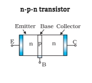
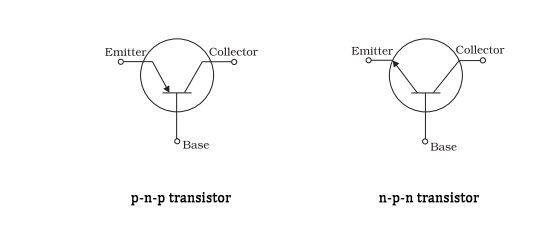
- n-p-n transistor: A p-type semiconductor (base) separates two segments of the n-type semiconductor (emitter and collector).
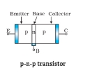
- p-n-p transistor: An n-type semiconductor (base) separates two segments of the p-type semiconductor (emitter and collector.
In the figure all three segments have different thickness and doping levels. The schematic symbols of both these transistors are as follows:
15. What are the current components?
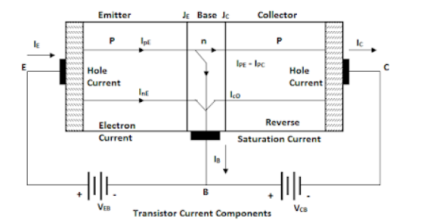
The transistor current components which flow across the forward biased emitter junction and the reverse biased collector junction.
- The emitter current IC component consists of hole current IpE (holes crossing from emitter into base) and electron current InE (electrons crossing from base into emitter).
- The ratio of hole to electron currents IpE/InE, crossing the emitter junctions in proportional to the ratio of the conductivity of p material to that of the n materials. Since the doping of the emitter is made much larger than the doping of the base, emitter current consists almost entirely of holes in p-n-p transistor.
- The holes crossing the emitter junction JE reach the collector junction JC because some of them combine with electrons in the n-type base. If IpC is the hole curretat JC, there must be a bulk recombination current IPE-IPC leaving the base, as shown in figure.
- If the emitter were open circuited, no carriers are injected from emitter into the base and emitter current IE=0. Under this condition, the collector-base junction JC acts as a reverse-biased diode and therefore , the collector current ICO would equal to the reverse saturation current ICO.
- Therefore, when emitter-base junction is forward biased and collector–base junction is reverse-biased, the total collector current will be sum of two currents. Hence
IC=IPC+ICBO ------> (a)
16. Explain transistor as an amplifier?
Transistor raises the strength of a weak signal and hence acts an amplifier. The transistor amplifier circuit is shown in the figure below.
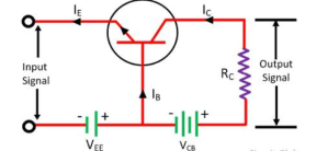
Transistor as an Amplifier
The transistor has three terminals namely emitter, base and collector. The emitter and base of the transistor are connected in forward biased and the collector base region is in reverse bias. The forward bias means the P-region of the transistor is connected to the positive terminal of the supply and the negative region is connected to the N-terminal and in reverse bias just opposite of it has occurred.
Vee is applied to the input circuit along with the input signal to achieve the amplification. The DC voltage VEE keeps the emitter-base junction under the forward biased condition regardless of the polarity of the input signal and is known as bias voltage.
When a weak signal is applied to the input, a small change in signal voltage causes a change in emitter current this change is almost the same in collector current because of the transmitter action.
In the collector circuit, a load resistor RC of high value is connected. When collector current flows through such a high resistance, it produces a large voltage drop across it. Thus, a weak signal (0.1V) applied to the input circuit appears in the amplified form (10V) in the collector circuit.
Input Resistance
When the input circuit is forward biased, the input resistance will be low. The input resistance is the opposition offered by the base-emitter junction to the signal flow.
Hence, it is the ratio of small change in base-emitter voltage (ΔVBE) to the resulting change in base current (ΔIB) at constant collector-emitter voltage.
Input resistance, Ri=ΔVBE/ΔIb
Where Ri = input resistance, VBE = base-emitter voltage, and IB = base current.
Output Resistance
The output resistance of a transistor amplifier is very high. The collector current changes very slightly with the change in collector-emitter voltage.
The ratio of change in collector-emitter voltage (ΔVCE) to the resulting change in collector current (ΔIC) at constant base current.
Output resistance = Ro=ΔVCE/ΔIC
Where Ro = Output resistance, VCE = Collector-emitter voltage, and IC = Collector-emitter voltage.
Current gain
It is the ratio of change in collector current (ΔIC) to the change in base current (ΔIB).
Current gain, β=ΔIC/ ΔIB
Voltage Gain
It is the ratio of change in output voltage (ΔVCE) to the change in input voltage (ΔVBE).
Voltage gain, AV=ΔVCE/ΔVBE
= ∆Ic x RAC / ∆ IB x Ri = ∆ Ic / ∆ Ib x RAC/ Ri = β x RAC / Ri
Power Gain
It is the ratio of output signal power to the input signal power.
Power gain Ap = (∆ Ic) 2 / (∆ IB)2 x RAC/ Ri
(∆Ic / ∆ IB) x ∆Ic x RAC/ Ri
= current gain x voltage gain
17. Explain CB,CE,CC configurations?
Common Base CB Configuration
Here the Base terminal is taken as common terminal for both input and output of the transistor. The common base connection for both NPN and PNP transistors is as shown in the following figure.
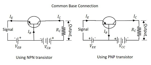
Let us consider NPN transistor in CB configuration. When the emitter voltage is applied, as it is forward biased, the electrons from the negative terminal repel the emitter electrons and current flows through the emitter and base to the collector to contribute collector current.
The collector voltage VCB is kept constant. In CB configuration, the input current is the emitter current IE and the output current is the collector current IC.
Current Amplification Factor α
The ratio of change in collector current ΔIC to the change in emitter current ΔIEwhen collector voltage VCB is kept constant, is called as Current amplification factor.
It is denoted by α.
α=ΔIC/ΔIEatconstantVCB
Expression for Collector current
Along with the emitter current flowing, there is some amount of base current IB which flows through the base terminal due to electron hole recombination. As collector-base junction is reverse biased, there is another current which is flown due to minority charge carriers. This is the leakage current which can be understood as Ileakage. This is due to minority charge carriers and hence small.
The emitter current that reaches the collector terminal isαIE
Total collector current
IC=αIE+Ileakage
If the emitter-base voltage VEB = 0 there flows a small leakage current, which can be termed as ICBO collector−basecurrentwithoutputopencollector−basecurrentwithoutputopen.
The collector current therefore can be expressed as
IC=αIE+ICBO
IE=IC+IB
IC=α(IC+IB)+ICBO
IC(1−α)=αIB+ICBO
IC=(α1−α)IB+(ICBO1−α)
IC=(α1−α)IB+(11−α)ICBO
Hence the above derived is the expression for collector current. The value of collector current depends on base current and leakage current along with the current amplification factor of that transistor in use.
Common Emitter CE Configuration
The name itself implies that the Emitter terminal is taken as common terminal for both input and output of the transistor. The common emitter connection for both NPN and PNP transistors is as shown in the following figure.
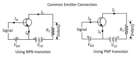
Just as in CB configuration, the emitter junction is forward- biased and the collector junction is reverse- biased. The flow of electrons is controlled in the same manner.
The input current is the base current IB and the output current is the collector current IC here.
Base Current Amplification factor β
The ratio of change in collector current ΔICto the change in base current ΔIB is known as Base Current Amplification Factor. It is denoted by β
β=ΔIC/ΔIB
Relation between β and α
The relation between base current amplification factor and emitter current amplification factor.
β=ΔIC/ΔIB
α=ΔIC/ΔIE
IE=IB+IC
ΔIE=ΔIB+ΔIC
ΔIB=ΔIE−ΔIC
We can write
β=ΔIC/∆IE−ΔIC
β=ΔIC/ΔIE/ΔIE/ΔIE−ΔIC/ΔIE
α=ΔIC/ΔIE
We have
α=ΔIC/ΔIE
Therefore,
β=α(1−α)
From the above equation, it is evident that, as α approaches 1, β reaches infinity.
Expression for Collector Current
In the Common Emitter configuration, IB is the input current and IC is the output current.
We know
IE=IB+IC
And
IC=αIE+ICBO
=α(IB+IC)+ICBO
IC(1−α)=αIB+ICBO
IC=α1−αIB+11−αICBO
If base circuit is open that is if IB = 0,
The collector emitter current with base open is ICEO
ICEO=11−αICBO
Substituting the value we get
IC=α1−αIB+ICEO
IC=βIB+ICEO
Hence the equation for collector current is obtained.
Common Collector CCConfiguration
The name itself implies that the Collector terminal is taken as common terminal for both input and output of the transistor. The common collector connection for both NPN and PNP transistors is as shown in the following figure.
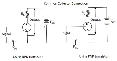
Just as in CB and CE configurations, the emitter junction is forward biased and the collector junction is reverse biased. The flow of electrons is controlled in the same manner. The input current is the base current IB and the output current is the emitter current IE here.
Current Amplification Factor γγ
The ratio of change in emitter current ΔIE to the change in base current ΔIB is known as Current Amplification factor in common collector CC configuration. It is denoted by γ.
γ=ΔIE/ΔIB
- The current gain in CC configuration is same as in CE configuration.
- The voltage gain in CC configuration is always less than 1.
Relation between γ and α
Let us try to draw some relation between γ and α
γ=ΔIE/ΔIB
α=ΔIC/ΔIE
IE=IB+IC
ΔIE=ΔIB+ΔIC
ΔIB=ΔIE−ΔIC
Substituting the value of IB, we get
γ=ΔIE/ΔIE−ΔIC
Dividing by ΔIE/ΔIE
γ=ΔIE/ΔIE/ΔIE/ΔIE−ΔIC/ΔE
1/1−α
γ=1/1−α
Expression for collector current
We know
IC=αIE+ICBO
IE=IB+IC
=IB+(αIE+ICBO)
IE(1−α)=IB+ICBO
IE=IB1−α+ICBO1−α
IC≅IE=(β+1)IB+(β+1)ICBO
The above is the expression for collector current.