HARCOURT BUTLER TECHNICAL UNIVERSITY
UNIT-4
MATERIALS OF TECHNOLOGICAL IMPORTANCE
QUESTION BANK
1 Question: Define dielectric constant?
Solution:
Dielectric constant it is a quantity measuring the ability of a substance to store electrical energy in an electric field.
Or
The ratio of the permittivity of the substance to the permittivity of the free space
Dielectric constant is also called Relative Permittivity Dielectric Constant is expressed by Greek letter kappa ‘κ’. It is dimensionless quantity.
It is mathematically expressed as:
κ= 
Where,
- κ is the dielectric constant
- 𝜺 is the permittivity of the substance
- 𝜺0 is the permittivity of the free space.
2 Question: Define polarization of a dielectric material?
Solution:
The diploe moment per unit volume of dielectric material is called the electric polarization of dielectric. It is represented by vector P.
In S.I. System, unit of polarization is C/m2.
3 Question: Define dielectric breakdown and dielectric strength.
Solution:
Whenever the electrical field strength applied to a dielectric exceeds a critical value, very large current flows through it. The dielectric loses its insulating property and becomes conducting. This phenomenon is known as dielectric breakdown.
The electrical field strength at which dielectric breakdown occurs is known as dielectricStrength.
4 Question: What are the differences between polar and non-polar molecules? Also discuss the effect of electric field on dielectric?
Solution:
Polar Molecules: Polar Molecules are those in which centre of gravity of positive and negative charge does not coincide with each other. This is because they all are asymmetric in shape. Examples: H2O, CO2, NO2 etc.
Non-Polar Molecule: Non-polar molecules are those in which centre of gravity of positive charge and negative charge coincide with each other. The molecule has zero dipole moment as they all are symmetric in shape. Examples: O2, N2, H2 etc.
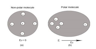
Response of Dielectric to External Electric Field
In case of Polar Molecules-When the electric field is not present, it causes the electric dipole moment of these molecules in a random direction. This is why the average dipole moment is zero. If the external electric field is present, the molecules align themselves in the direction electric field and resulted in having dipole moment.
In case of Non-Polar Molecules– As we know nonpolar molecule has zero dipole moment. In spite of zero dipole, when a dielectric nonpolar material is placed in an electric field. The positive and the negative charges in a nonpolar molecule experience forces in opposite directions. This force causes the separation between the charges and hence nonpolar molecule experiences induced dipole moment.
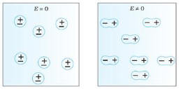
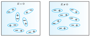
Figure a (left) Non Polar Molecule Figure b (right) Polar Molecule
5 Question: Dipoles are created when dielectric is placed in __________
a) Magnetic Field
b) Electric field
c) Vacuum
d) Inert Environment
Solution:
b
When the dielectric is placed in an electric field, like between the parallel plates of a capacitor, the dipoles are created and they tend to align themselves parallel to the direction of the electric field.
6 Question: Show that Electronic polarization depends upon radius of atom?
Or
Show that Electronic polarization depends upon volume of atom?
Solution:
Electronic polarization refers to the separation of centre of positive charge and centre of negative charge in a material.This separation is caused by high electric field.
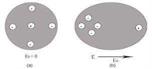
Figure (a) shows thecharge distribution of an atom in absence of electric field while figure (b) show the charge distribution in presenceof external electrical field.
Let us consider a single atom of atomic number Z. +e coulomb is the charge of each proton in the nucleus and -e coulomb is the charge of each electron surrounds the nucleus. All electrons in the atom form a spherical cloud of negative charge surrounds the positively charged nucleus. The charge of nucleus is +Ze coulombs and charge of the negative cloud of electrons is -Ze coulombs.
Let us also assume that the negative charge of the electrons cloud is homogeneously distributed on a sphere of radius R. In the absence of external electric field, the center of this sphere and center of nucleus of the atom coincide.
When an external electric field E is applied to the atom. Because of this external electric field the nucleus of the atom is shifted towards negative intensity of the field and the electron cloud is shifted towards the positive intensity of the field.
As due to influence of external electric field the center of nucleus and center of electrons cloud are separated, there will be an attractive force between them according to Coulomb’s law.
Let us suppose x is distance of separation between positive charge nucleus and electron cloud.
Also Nucleus is considered as point charge. Hence, the electrostatic force acting on the nucleus =+EZe …….(1)
As we know nucleus has been shifted from the center of electrons cloud by a distance x.
By using Gauss’s theorem
The force is only due to electron cloud acting upon nucleus would only be due to the portion of the cloud enclosed by the sphere of radius x. Portion outside the sphere of radius x does not apply any force on the nucleus.
Volume of the sphere of radius x = (4/3)πx3and
Volume of the sphere of radius R = (4/3)πR3
Now total negative charge of the electron cloud is -Ze…..(2)
Hence, the quantity of negative charge enclosed by the sphere of radius x is,
[-Ze/(4/3)πR3] * (4/3)πx3= -Ze (x3/ R3)……..(3)
According to coulomb’s law = q1q2 /4 πR2
Here it becomes charge on electrons q1=-Ze (x3/ R3)
Charge on nucleus q2= Ze
So coulomb’s force = {-Ze (x3/ R3) * Ze}/4πƐox2 = Z2e2x/4πƐo R3……(4)
Note- magnitude is taken into account. Neglect negative sign.
i.e. At equilibrium Electrostatic force = Coulomb force .
EZe = Z2e2x/4πƐoR3……..(5)
Upon simplify
x = {4πƐoR3/Ze} E
Now dipole moment = either charge * separation between charges i.e. x
= Ze *{4πƐoR3/Ze} E
= 4πƐoR3E
Polarization is number of dipole moment per unit volume. Let us suppose N is the number of dipoles per unit volume so
Pe=4πƐoR3EN
So it is clear that polarization depends upon radius of atom or volume of atom and number of atoms present per unit volume.
7 Question: Explain Ionic polarization ? Derive relation for it?
Solution:
Ionic polarization occurred only in that dielectric material in which atoms contain ionic bonds. When such a material is placed in an external electric field the separation between positive charge and negative charge is separated through larger distance as compared to original length.
NaCl and KCl molecule shows ionic polarization occurs. In this polarization the net electric field is zero.
Sodium chloride (NaCl) molecule is formed by ionic bond between sodium and chlorine atoms. Due to electrostatic force between positive sodium and negative chlorine ions, they bound together and form sodium chloride molecule. Because of the presence of inter nucleus distance in the sodium chloride molecule, one might think that an ionic crystal would possess polarization even in the absence external electric filed. Since each pair constitute an electric dipole. But this is not so due to lattice symmetry these dipoles cancel each other’s effect.
Figure of NaCl crystal
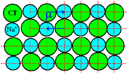
As NaCl have only two atoms or ions there must be a single dipole moment pointing from negative to positive ion in each molecule. But there exists other ionic compounds having more than two atoms.
Number of dipole moments is directly proportional to the number of bonds in a molecule. But all the dipole moments are directed from relatively negative ion to positive ion. The resultant dipole moment of a single molecule would be the vector sum of individual dipole moments of the molecule.
In absence of electric field E, the distance between the ions is d but in presence of electric field, distances between the ions increases.
Figure of NaCl in the presence of electric field
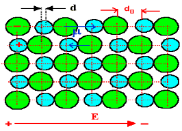
In the presence of electric field we have certain amount of dipole moment.
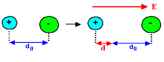
Hence force F1 due to electric field is
F1=qE ……(1)
Where q is the net charge on ion.
F2 restoring force due to binding force between ions
F2=kd…..(2)
Where k is spring constant. Here we are considering bond as spring.
k may also expressed in terms of other constant which is related to the shape of interatomic potential as young’s modulus or modulus of rigidity as
k=Ydo …..(3)
At Equilibrium F1 = F2 at equilibrium distance d
QE = kd
QE = Ydod using (3)
d = qE/Ydo
Now dipole moment p= qd = q2E/Ydo…..(4)
And polarization Pi = Nq2E / Ydo……(5)
This is called ionic polarization. This can also be expressed as
Pi =NαiE
Where αi is constant of proportionality known as ionic polarizability constant. This polarization is independent of temperature.
8 Question: Explain Orientational Polarization? Derive relation for it?
Solution:
Polar dielectric exhibit orientational polarization. In the absence of electric field, the orientation of the molecule are random and hence the net dipole moment is zero when external force is applied the dipole tried to align themselves along the direction of the applied field. This type of polarization is known as orientational polarization.
Ionic polarization: Orientational polarization: This occurs due to the permanent dipole moment in a material. It occurs in elements such as HCl and H2O.
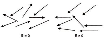
Potential energy U of the dipole moment making an angle θwith the electric field.Where p0 is the dipole moment.
U=−p0⋅E=−p0Ecosθ
According to statistical mechanics, the number of dipoles or molecules making an angle with the electric field is proportional to
e−U/kT
Letting n(θ) be the number of molecules per unit solid angle at θ, we have
n(θ)=n0e+p0Ecosθ/kT
For normal temperatures and fields, the exponent is small, so we can approximate by expanding the exponential:
n(θ)= n0 (1+p0EcosθkT)
To findn0 , we integrate over all angles and the result is equal to N.
Where N is the total number of molecules per unit volume. The average value of cosθ over all angles is zero, so the integral is just n0 times the total solid angle 4π. We get
n0=N4π or N= n0 /4π
There exits molecules along the field (cosθ=1) than against the field (cosθ=−1). So in any small volume containing many molecules there will be a net dipole moment per unit volume.
As dipole moment is present so polarization Pdis given
Pd =∑unitvolumep0cosθi
Evaluate Total Polarization over solid angle 2πsinθdθ. We have to integrate it
Pd = 0∫πn(θ)p0cosθ2πsinθdθ
Substitute the value of n(θ)
Pd = −N/2 −1∫1 {1+(p0E/kT)cosθ)p0cosθd(cosθ)
By integrating we get,
Pd =Np02E/ 3kT
The polarization is proportional to the field E and depends inversely on the temperature, because at higher temperatures there is more randomness by collisions.
This can also be expressed as
Pd =αdE
Where αd is called dipolar or orientation polarizability and it is equal to p02/ 3kT.
9 Question: Distinguish between conductor, insulator and semiconductor?
Solution:
We can distinguish between conductor, insulator and semiconductor by the Band Model
Bands are formed by the closely spaced orbitals.
There are three types of bands:
1. Valance Bands:Valence band it is a group of orbitals which contain electrons in the shell. Or we can sayIt is also defined as the energy band that comprises of valence electrons present in the outermost shell of an atomic structure.
These valence electrons, when provided with sufficient energy, get changed into free electrons and moves to conduction band thereby causing conductivity. It is at a lower energy level than the conduction band in the energy level diagram.
2. Conduction Band: Conduction band is a group of empty orbitals of the shells that do not contain any electron due to their configuration making the orbitals of higher energy levels.
When the electrons pass from valance band to the conduction band these solids conduct electricity with flow of charges in the form of electrons.
3. Forbidden Energy Band: These two bands are separated by a certain amount of energy known as the forbidden energy gap. In this band not a single electron is available. It diagram it is named as Band Gap.
Let us distinguish between conductor, semiconductors and insulator on the basis of these bands.
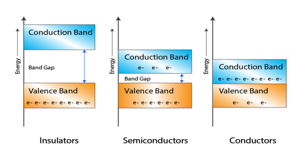
- In Conductors: The valance band and the conduction band overlap each other. This makes it easy for the electricity to pass through them. In conductors, the valence band is either not fully occupied with electrons, or the filled valence band overlaps with the empty conduction band. In general, both states occur at the same time, the electrons can therefore move inside the partially filled valence band or inside the two overlapping bands. In conductors there is no band gap between the valence band and conduction band.
- InSemi-conductors: there is a slight gap between the conduction band and the valance band. This band gap is less than or equal to 1.4eV. The electrons from valance shell take a little energy to excite from valance band to the conduction band.Even in semiconductors, there is a band gap, but compared to insulators it is so small that even at room temperature electrons from the valence band can be lifted into the conduction band. The electrons can move freely and act as charge carriers.
- InInsulators: In insulators the valence band is fully occupied with electrons due to the covalent bonds.To achieve conductivity, electrons from the valence band have to move into the conduction band.the energy gap is considerably large and the electrons of the valance band cannot be excited to the conduction band before the melting or the dissociation of the solid. This means that under the practically ambient condition it cannot conduct electricity.
10Question: Discuss conduction in intrinsic semiconductor?
Solution:
Intrinsic Semiconductor
- An intrinsic type of semiconductor material made to be very pure chemically. As a result it possesses a very low conductivity level having very few number of charge carriers, namely holes and electrons, which it possesses in equal quantities.
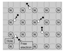
- The most commonly used semiconductor basics material by far is silicon. Silicon has four valence electrons in its outermost shell which it shares with its neighbouring silicon atoms to form full orbital’s of eight electrons. The structure of the bond between the two silicon atoms is such that each atom shares one electron with its neighbour making the bond very stable.
- As there are very few free electrons available to move around the silicon crystal, crystals of pure silicon (or germanium) are therefore good insulators. Silicon atoms are arranged in a definite symmetrical pattern making them a crystalline solid structure. A crystal of pure silica (silicon dioxide or glass) is generally said to be an intrinsic crystal (it has no impurities) and therefore has no free electrons.
- An extremely pure semiconductor is called as Intrinsic Semiconductor. On the basis of the energy band phenomenon, an intrinsic semiconductor at absolute zero temperature is shown below.
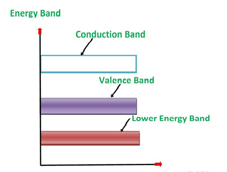
- Its valence band is completely filled and the conduction band is completely empty. When the temperature is raised and some heat energy is supplied to it, some of the valence electrons are lifted to conduction band leaving behind holes in the valence band as shown below.
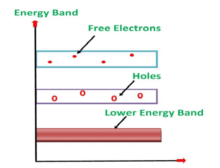
- A hole is the absence of an electron in a particular place in an atom. Although it is not a physical particle in the same sense as an electron, a hole can be passed from atom to atom in a semiconductor material. It is considered to have positive charge. Holes are positive charge carriers.
- The electrons reaching at the conduction band move randomly. The holes created in the crystal also free to move anywhere.
- This behaviour of the semiconductor shows that they have a negative temperature coefficient of resistance. This means that with the increase in temperature, the resistivity of the material decreases and the conductivity increases.
- But simply connecting a silicon crystal to a battery supply is not enough to extract an electric current from it. To do that we need to create a “positive” and a “negative” pole within the silicon allowing electrons and therefore electric current to flow out of the silicon. These poles are created by doping the silicon with certain impurities.
11 Question: What is doping? Discuss its importance in semiconductor?
Solution:
Doping
The process by which an impurity is added to a semiconductor is known as Doping. The amount and type of impurity which is to be added to a material has to be closely controlled during the preparation of extrinsic semiconductor. Generally, one impurity atom is added to a 108 atoms of a semiconductor.
The purpose of adding impurity in the semiconductor crystal is to increase the number of free electrons or holes to make it conductive.
If a Pentavalent impurity, having five valence electrons is added to a pure semiconductor a large number of free electrons will exist. Which make a n-type extrinsic semiconductor.
If a trivalent impurity having three valence electrons is added, a large number of holes will exist in the semiconductor. Which make a p-type extrinsic semiconductor.
12 Question: What is P-type Extrinsic Semiconductor? Draw its energy level diagram and discuss the conduction mechanism in p type semiconductor?
Solution:
P-type Extrinsic Semiconductor
The extrinsic p-Type Semiconductor is formed when a trivalent impurity is added to a pure semiconductor in a small amount, and as a result, a large number of holes are created in it. A large number of holes are provided in the semiconductor material by the addition of trivalent impurities like Gallium and Indium. Such type of impurities which produces p-type semiconductor are known as an Acceptor Impurities because each atom of them create one hole which can accept one electron.
In a P-type semiconductor material there is a shortage of electrons, i.e. there are 'holes' in the crystal lattice. Electrons may move from one empty position to another and in this case it can be considered that the holes are moving. This can happen under the influence of a potential difference and the holes can be seen to flow in one direction resulting in an electric current flow. It is actually harder for holes to move than for free electrons to move and therefore the mobility of holes is less than that of free electrons. Holes are positively charged carriers.
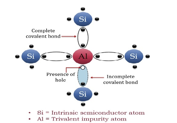
A trivalent impurity like Aluminium, having three valence electrons is added to Silicon crystal in a small amount. Each atom of the impurity fits in the Silicon crystal in such a way that its three valence electrons form covalent bonds with the three surrounding Silicon atoms as shown in the figure below.
Energy Band Diagram of p-Type Semiconductor
The energy band diagram of a p-Type Semiconductor is shown below.
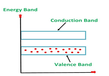
A large number of holes or vacant space in the covalent bond is created in the crystal with the addition of the trivalent impurity. A small or minute quantity of free electrons is also available in the conduction band.
They are produced when thermal energy at room temperature is imparted to the Silicon crystal forming electron-hole pairs. But the holes are more in number as compared to the electrons in the conduction band. It is because of the predominance of holes over electrons that the material is called as a p-type semiconductor. The word “p” stands for the positive material.
Conduction Through p Type Semiconductor
In p type semiconductor large number of holes are created by the trivalent impurity. When a potential difference is applied across this type of semiconductors.
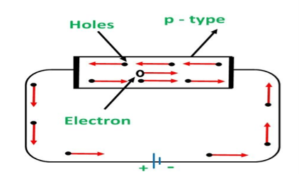
The holes are available in the valence band are directed towards the negative terminal. As the current flow through the crystal is by holes, which are carrier of positive charge, therefore, this type of conductivity is known as positive or p type conductivity. In a p type conductivity the valence electrons move from one covalent to another.
The conductivity of n type semiconductor is nearly double to that of p type semiconductor. The electrons available in the conduction band of the n type semiconductor are much more movable than holes available in the valence band in a p type semiconductor. The mobility of holes is poor as they are more bound to the nucleus.
Even at the room temperature the electron hole pairs are formed. These free electrons which are available in minute quantity also carry a little amount of current in the p type semiconductors.
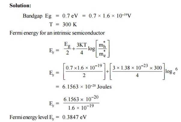
13Question: For an intrinsic Semiconductor with a band gap of 0.7 eV, determine the position of EF at T = 300 K if m*h = 6m*e
Solution:
14 Question: What is N-type Extrinsic Semiconductor? Draw its energy level diagram and discuss the conduction mechanism in N type semiconductor?
Solution:
N-typeExtrinsic Semiconductor
When a few Pentavalent impurities such as Phosphoruswhose atomic number is 15, which is categorised as 2, 8 and 5. It has five valence electrons, which is added to silicon crystal. Each atom of the impurity fits in four silicon atoms as shown in the figure below.
Hence, each Arsenic atom provides one free electron in the Silicon crystal. Since an extremely small amount of Phosphorus, impurity has a large number of atoms; it provides millions of free electrons for conduction.
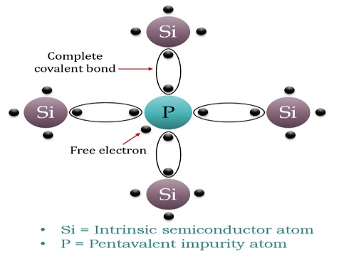
An N-type semiconductor material has an excess of electrons. In this way, free electrons are available within the lattices and their overall movement in one direction under the influence of a potential difference results in an electric current flow. This in an N-type semiconductor, the charge carriers are electrons.
Energy Diagram of n-Type Semiconductor
A large number of free electrons are available in the conduction band because of the addition of the Pentavalent impurity. These electrons are free electrons which did not fit in the covalent bonds of the crystal. However, a minute quantity of free electrons is available in the conduction band forming hole- electron pairs.
The Energy diagram of the n-type semiconductor is shown in the figure below.
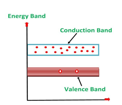
- The addition of pentavalent impurity results in a large number of free electrons.
- When thermal energy at room temperature is imparted to the semiconductor, a hole-electron pair is generated and as a result, a minute quantity of free electrons is available. These electrons leave behind holes in the valence band.
- Here n stands for negative material as the number of free electrons provided by the pentavalent impurity is greater than the number of holes.
Conduction Through n-Type Semiconductor
In the n-type semiconductor, a large number of free electrons are available in the conduction bands which are donated by the impurity atoms. The figure below shows the conduction process of an n-type semiconductor.
When a potential difference is applied across this type of semiconductor, the free electrons are directed towards the positive terminals. It carries an electric current. As the flow of current through the crystal is constituted by free electrons which are carriers of negative charge, therefore, this type of conductivity is known as negative or n-type conductivity.
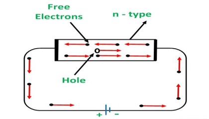
The electron-hole pairs are formed at room temperature. These holes which are available in small quantity in valence band also consist of a small amount of current. For practical purposes, this current is neglected.
15Question: Derive expression for carrier concentration for intrinsic semiconductors? Explain Fermi level for Intrinsic semiconductors and what is the effect of temperature on Fermi level?
Solution:
Intrinsic semiconductors—carrier concentration
Here we will calculate the number of electrons excited into conduction band at temperature T and also the hole concentration in the valence band. It is assumed that the electrons in the conduction band behave as if they are free particles with effective mass me* and the holes near the top of the valence band behave as if they are free particles with effective mass mh*.
Here we will calculate the electron concentration, hole concentration
Density of Electrons in Conduction Band
The number of free electrons per unit volume of semiconductor having energies in between E and E + dE is represented as N(E) dE
DE = width of Energy band
Therefore, we have:
N(E) dE = ge(E) dE fe(E) ……….(1)
ge(E) = The density of electron states per unit volume
fe(E) = Fermi-Dirac distribution function i.e. probability that an electron occupies an electron state
The number of electrons present in the conduction band per unit volume of material ‘n’ is obtained by integrating N(E) dE between the limits Ec and Ect
Where Ec = the bottom energy levels of conduction band
Ect = the bottom and top energy levels of conduction band
n =  ……….(2)
Can be written as
n =  =
= 
n =  -
-  ……….(3)
We know that above Ect, there is no electrons.
Hence, Equation (3) becomes
n =  -
- 
n =  ……….(4)
The Fermi-Dirac distribution function fe(E) can be represented as:
 (E) =
(E) = ……….(5)
Compared to the exponential value, so the ‘1’ in the denominator can be neglected.
So  >>1
>>1
Hence,  (E) =
(E) = =
=  ……….(6)
The density of electron states ge(E) in the energy space from E = 0 to E can be written as:
 (E) =
(E) =  [
[ ]3/2 (E - 0) ½ ……….(7)
Where me* is the effective mass of an electron and h is Planck’s constant.
 (E)dE =
  [
[ ]3/2 (E - 0) ½dE……….(8)
To evaluate n, the density of states is counted from Ec, since the minimum energy state in conduction band is Ec. So eq (8) can become
 (E)dE =
  [
[ ]3/2 (E - Ec) ½dE……….(9)
Substituting Equations (6) and (9) in (4) gives
n =  3/2 (E-
 )1/2
)1/2 dE
dE
n = [
[ ]3/2
]3/2 1/2
1/2 dE………… (10)
The above equation can be simplified by the following substitution:
Put ɛ = E −Ec ………… (11)
So, dɛ = dE
In Equation (11), Ec is constant, as we change the variable E to ε in Equation (10), the integral limits also change.
In Equation (11), as E → Ec then ε → 0 and E →∞, then ε also →∞.
The exponential term in Equation (10) becomes:
 = exp [
 ] = exp [
 ]
]
 ………… (12)
Substituting Equations (11) and (12) in (10), we get:
n = [
[ ]3/2
]3/2 dE
dE
n = [
[ ]3/2
]3/2 dE………… (13)
Above integral (I) can be simplified by substitution. Put ε = x2
So that dɛ = 2x dx
I = 2x dx
2x dx
= dx
dx
= =
= T)3/2………… (14)
Substituting Equation (14) in (13) gives:
n = [
[ ]3/2
]3/2 T)3/2
T)3/2
n =
n = 
n =  ………… (15)
The term  is almost a constant compared with the exponential term as the temperature changes. So, it is a pseudo constant and is given by the symbol Nc. So, we have
n =Nc ………… (16)
Density of Holes in Valence Band
The number of holes per unit volume of semiconductor in the energy range E and E + dE in valence band is represented as P(E) dE. Proceeding same way( as in case of electrons) we have
Therefore, we have:
P(E) dE = gh(E) dE fh(E) ……….(17)
DE = width of Energy band
gh(E) = The density of holes states per unit volume
fh(E) = Fermi-Dirac distribution function i.e. probability that an hole occupies an electron state
The number of electrons present in the conduction band per unit volume of material ‘n’ is obtained by integrating P(E) dE between the limits Evb and EV
Where EV = the bottom energy levels of valence band
Evb = the bottom and top energy levels of valence band
The total number of holes present in the valence band per unit volume of material ‘p’ is obtained by integrating P(E) dE
 ……….(18)
Equation (18) can be represented as:
 ……….(19)
Now we know that below Evb no holes is present. Hence, Equation (19) becomes
 ……….(20)
We know hole can also be defined as absence of an electron.
Presence of a hole = the absence of an electron
Hence, the Fermi-Dirac function of holes fh(E) in the valence band is:
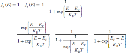
Compared to exponential, the ‘1’ in the denominator is negligible,

Hence,
 ……….(21)
The density of hole states between E and E + dE in valence band can be written similar to Equation (8.9) for electrons.
 ……….(22)
Where mh* is the effective mass of hole.
Substituting Equations (21) and (22) in (20),
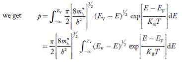 ……….(23)
The above equation can be simplified by the substitution:
Put ɛ = EV − E ............. (24)
So dɛ = −dE
In Equation (24), EV is constant, as we change the variable E to ε in Equation (23), the integral limits also change.
In Equation (24),
As E → EV then ε → 0
And E→−∞, then ε →∞
The exponential term in Equation (23) becomes:
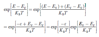 ............. (25)
Substituting Equations (24) and (25) in (23), we get:
 ………….(26)
From Equation (14), we know the integral value  T)3/2 put here and we get
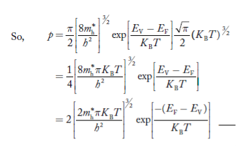 ………….(27)
….The term  is almost constant compared with the exponential term as the temperature changes. So, it is a pseudo constant and is given by the symbol NV. So, we have
 …………… (28)
16Question: Explain Fermi level for Intrinsic semiconductors and what is the effect of temperature on Fermi level?
Solution:
Fermi Level
We know that in intrinsic semiconductor
Electron concentration ‘n’ = Hole concentration ‘p’
Equating Equations (15) and (27), we get
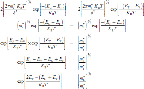
Taking logarithms on both sides, we get
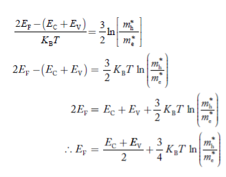 ……………… (29)
Normally, mh* is greater than me*, since ln  is very small so that EF is just lie in the middle of energy gap
Temperature effect on Fermi level
Fermi level slightly rises with increase of temperature.
But in case of pure intrinsic semiconductor like Si and Ge,
mh* ≈ me*
So in these cases Fermi level lies at the middle of energy gap.
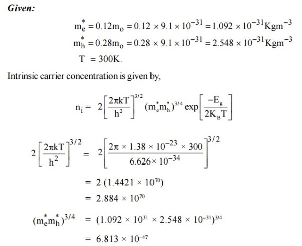
17Question: Calculate the intrinsic concentration of charge carriers at 300 K given that m *e =0.12m o ,m*h =0.28mo and the value of brand gap = 0.67 eV.
Solution:
18 Question: Where Fermi level lie in case of p type and n type extrinsic semiconductor?
Or
Derive expression for Carrier Concentration in Extrinsic Semiconductors.
Solution:
Carrier Concentration in Extrinsic Semiconductors
The number of charge carriers present per unit volume of a semiconductor material is called carrier concentration.
Suppose donor and acceptor atoms are doped in a semiconductor.
At temperature T K,
n = number of conduction electrons
p = number of holes
N−A = number of acceptor ions
N+D = number of donor ions
We know that the below equation hold good in semiconductor. The total negative charge due to conduction electrons and acceptor ions is equal to holes and donor ions in unit volume of material.
So the material will be considered neutral if,
n + N−A = p + N+D ……….(34)
Equation (34) is called charge neutrality equation.
In the above equation
 ………..(35)
Concentration of acceptor ions N−A = acceptor concentration x probability of finding an electron in acceptor level
 ………..(36)
Similarly, the donor ions concentration is

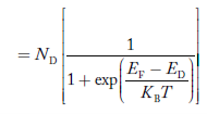 ………..(37)
In n-type material
Note
nn represents electrons in n-type material
pn represents holes concentration in n-type material.
There are no acceptor atoms so N−A = 0.
At 0 K, all the electron states in donor level are occupied by electrons.
As the temperature is increased from 0 K, some of the electrons jump from these donor states into the conduction band.
Also the concentration of holes is extremely less compared with the concentration of conduction electrons [p << n]
From Equation (34) we have
n = p N+D
(Or) n ≈ N+D …………(38) [since p << N+D]
At temperature T K,
As the temperature increase Almost all the donor atoms donate electrons to conduction band.
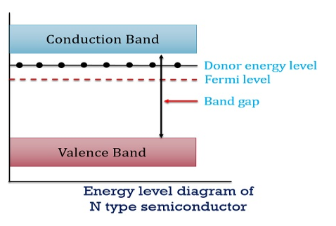
So, in n-type material, the free electron concentration is almost equal to the donor atoms.
So we can rewrite the above equation as
nn ≈ ND …………….(39)
Where nn represents electrons in n-type material
Also the hole concentration in n-type material can be obtained by applying law of mass action nn pn =ni2
 …………..(40)
Where pn represents holes concentration in n-type material.
In n-type material at 0 K, the Fermi energy level lies in the middle of Ec and ED

At temperature> 0K
 ……….(41)
With increase in temperature the Fermi level shifts upwards according to Equation (61) slightly due to ionization of donor atoms.
With further increase of temperature, electron-hole pairs are generated due to the breaking of covalent bonds, hence Fermi level shifts downwards.
In p-type semiconductor
Note
pp represents holes in p-type material
np represents electrons in p-type material
There are no donor atoms so means no ions present  = 0.
= 0.
At 0 K, all the acceptor levels are not occupied by electrons.
As the temperature is increased from 0 K, some electrons jump from top valence band energy levels to the acceptor states, leaving holes in the valence band and acceptor ions  are formed.
At some room temperature T K, concentration of conduction electrons is extremely less compared with hole concentration.
∴ From Equation (34), we have
n + N−A = p ……………(42)
(or) N−A ≈ p ……………. (43) [since n << N−A]
At temperature T K, in p-type material,
The hole concentration is almost equal to the acceptor atoms in unit volume of the material.
So, Equation (43) can be written as
pp ≈ NA……………….(44)
Where pp represents holes in p-type material
The electron concentration in p-type material can be obtained by applying law of mass action as nppp = ni2
 …………….(45)
Where np represent free electron concentration in p-type material.
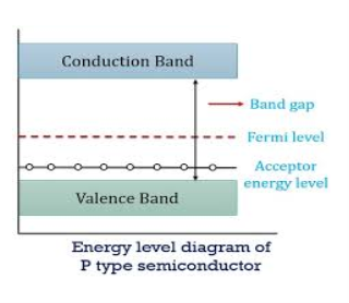
In p-type material, the Fermi level lies in between EV and EA at 0 K

As the temperature is increased from 0 K, the Fermi level shifts downwards slightly as per Equation (46) due to ionization of acceptor atoms.
And with further increase of temperature, electron-hole pairs are generated due to the breaking of covalent bonds, so Fermi level shifts upwards.
19 Question: Write physical and chemical properties of nanomaterials ?
Solution:
Physical properties
Inter atomic distance: When the material size is reduced to Nano scale, surface area to volume ratio increases. Due to increase of surface of surface area, more number of atoms will appear at the surface of compared to those inside. So Interatomic spacing decreases with size.
Thermal properties: Nano materials are different from that of bulk materials. The Debye Temperature and ferroelectric phase transition temperature are lower for nano materials. The melting point of nano gold decreases from 1200 K to 800K as the size of particle decreases form 300Å to 200Å.
Optical properties: Different sized nano particles scatters different of light incident on it and hence they appear with different colours. For example nano gold does not act as bulk gold. The nano particles of gold appear as orange, purple, red or greenish in colour depending on their grain size. The bulk copper is opaque whereas nanoparticle copper is transparent.
Magnetic properties: The magnetic properties of nano materials are different from that of bulk materials. In explaining the magnetic behaviour of nanomaterials, we use single domains unlike large number of domains in bulk materials. The coercivity value of single domain is very large.
For example, Fe,Co, and Ni are ferromagnetic in bulk but they exhibit super par magnetism. Na, K, and Rh are paramagnetic in bulk but they exhibit ferro-magnetic. Cr is anti-ferromagnetic in bulk but they exhibit super paramagnetic.
Mechanical properties: The mechanical properties such as hardness, toughness, elastic modulus, young’s modulus etc., of nano materials are different from that of bulk materials. In metals and alloys, the hardness and toughness are increased by reducing the size of the nano particles. In ceramics, ductility and super plasticity are increased on reducing grain size. Hardness increases 4 to 6 times as one goes from bulk Cu to nanocrystalline and it is 7 to 8 times for Ni.
Chemical properties
Nanocrystalline materials are strong, hard, erosion and corrosion resistant. They are chemically active and have the following chemical properties.
1. In electrochemical reactions, the rate of increase in mass transport increases as the particle size decreases.
2. The equilibrium vapour pressure, chemical potentials and solubilites of nanoparticles are greater than that for the same bulk material.
3. Most of the metals do not absorb hydrogen. But the hydrogen absorption increases with the decrease of cluster size in Ni, Pt and Pd metals.
20Question: Hownanomaterial can differentiate from bulk material?
Solution:
When the material size of the object is reduced to nanoscale, then it exhibits different properties than the same material in bulk form. The factors that differentiates the nanomaterials from bulk material is
1. Increase in surface area to volume ratio
2. Quantum confinement effect
Increase in surface area to volume ratio: The ratio of surface area to volume ratio is large for nano materials.
Example 1: To understand this let us consider a spherical material of radius ‘r’. Then its surface area to volume ratio is 3/r. Due to decrease of r, the ratio increases predominantly.
Example 2: For one cubic volume, the surface ratio is 6m2. When it is divided into eight cubes its surface area becomes 12m2. When it is divided into 27 cubes its surface area becomes 18m2. Thus, when the given volume is divided into smaller pieces the surface area increases.

Due to increase of surface of surface area, more number of atoms will appear at the surface of compared to those inside. For example, a nanomaterial of size 10nm has 20% of its atoms on its surface and 3nm has 50% of its atoms. This makes the nanomaterials more chemically reactive and affects the properties of nanomaterials.
Quantum confinement effect: According to band theory, the solid atoms have energy bands and isolated atoms possess discrete energy levels. Nano materials are the intermediate state to solids and atoms. When the material size is reduced to nanoscale, the energy levels of electrons change. This effect is called quantum confinement effect. This affects the optical, electrical and magnetic properties of nanomaterials.
21Question: Discuss Bottom up approach?
Solution:
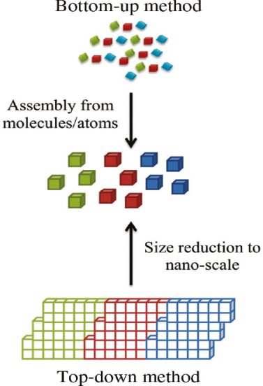
In bottom-up approaches nanomaterials are assembled from basic building blocks, such asmolecules or nanoclusters. The basic building blocks, in general, are nanoscaleobjects with suitable properties that can be grown from elemental precursors. The conceptof the bottom-up approach is that the complexity of nanoscale components should residein their self-assembled internal structure, requiring as little intervention as possible intheir fabrication from the macroscopic world.
The bottom-up approach uses atomic or molecular feed-stocks as thesource of the material to be chemically transformedinto larger nanoparticles. This has the advantage of being potentially much more convenientthan the top downapproach. By controlling the chemical reactionsand the environment of thegrowing nanoparticle, then the size, shape and composition of the nanoparticlesmay all be affected. For this reason nanoparticles produced by bottom up,chemically based and designed, reactions are normally seen as being of higherquality and having greater potentialapplications. This has ledto the growthof a host of common bottom up strategies for the synthesis ofnanoparticles.Many of these techniques can be tailoredto be performed in gas,liquid, solid states, hence the applicability of bottom-upstrategies to a wide range of end products. Most of the bottom up strategies requiressuitableorganometallic complexes or metal salts to be used as chemicalprecursors,which are decomposed in a controlled manner resulting in particle nucleation and growth. One of the key differences that can be used to subdividethese strategies into different categories is the method by which the precursor is decomposed.
A typical example of bottom-up is processing for nanocompositemagnets from individual high-magnetization and high-coercivity nanoparticles. The assembling critically depends on availability of anisotropic (single crystal) hard magneticnanoparticles. Anisotropic nanoparticles produced via surfactant-assisted high energy ballmilling satisfy the major requirements for this application.
22Question: Discuss Top down approach?
Solution:
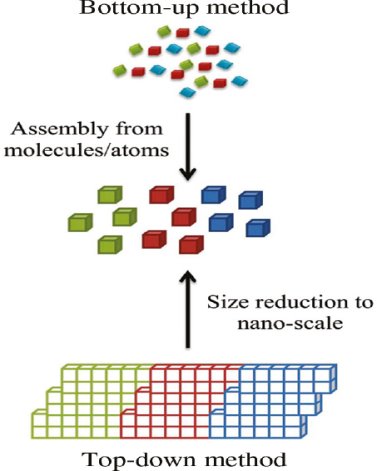
In top-down approaches, a bulk material is restructured (i.e. partially dismantled, machined, processed or deposited) to form nanomaterials. The aggressive scalingof electronic integrated circuits in recent years can be considered the greatest successof this paradigm. For top-down methods, the challenges increase as devices size is reduced and as the desired component designs become larger and more complex. Also thetop-down assembly of nanocomponents over large areas is difficult and expensive.
The top-down method involves the systematic breakdown of abulkmaterial into smaller unitsusing some form of grinding mechanism. This isbeneficialand simple to executeand avoids the use of volatile and poisonouscompounds frequentlyfound in the bottom-up techniques. However, the quality of thenanoparticles formedby grinding is accepted to be poor in comparisonwith the material produced by modern bottom up methods. The main drawbacksinclude defectproblems from grinding equipment, low particle surfaceareas, asymmetricalshape and size distributions and high energy neededto produce relatively small particles. Apartfrom these disadvantages,itmust be distinguishedthat the nano-material produced from grinding still finds use, due tothe simplicity of its manufacture, in applications including magnetic,catalyticandstructural properties.
23Question: Write applications of nanomaterials?
Solution:
Nano materials possess unique and beneficial, physical, chemical and mechanical properties; they can be used for a wide verity of applications.
Material technology
- Nanocrystalline aerogel are light weight and porous, so they are used for insulation in offices homes, etc.
- Cutting tools made of Nano crystalline materials are much harder, much more wear- resistance, and last stranger.
- Nano crystalline material sensors are used for smoke detectors, ice detectors on air craft wings, etc.
- Nano crystalline materials are used for high energy density storage batteries.
- Nano sized titanium dioxide and zinc dioxide is used in sunscreens to absorb and reflect ultraviolet rays.
- Nano coating of highly activated titanium dioxide acts as water repellent and antibacterial.
- The hardness of metals can be predominately enhanced by using nanoparticles.
- Nanoparticles in paints change colour in response to change in temperature or chemical environment, and reduce the infrared absorption and heat loss.
- Nano crystalline ceramics are used in automotive industry as high strength springs, ball bearings and valve lifters.
Information technology
- Nanoscale fabricated magnetic materials are used in data storage
- Nanocomputer chips reduce the size of the computer.
- Nano crystalline starting light emitting phosphors are used for flat panel displays.
- Nanoparticles are used for information storage.
- Nanophotonic crystals are used in chemical optical computers.
Biomedical
- Biosensitive nanomaterials are used for ragging of DNA and DNA chips.
- In the medical field, nanomaterials are used for disease diagnosis, drug delivery and molecular imaging.
- Nano crystalline silicon carbide is used for artificial heart valves due to its low weight and high strength.
Energy storage
- Nanoparticles are used hydrogen storage.
- Nano particles are used in magnetic refrigeration.
- Metal nanoparticles are useful in fabrication of ionic batteries.
24Question: Write a short note on Carbon nanotubes?
Solution:
Carbon nanotubes: Carbon nanotubes were first observed b SunminoIijima in 1911. Carbon exists in a large number of allotropic forms. These includes diamond, graphite and fullerenes (such as C60 , C70 etc.,). Carbon nanotubes are obtained by rolling the graphite sheet into tubes with the bonds at the ends of the sheet. These bonds are used to close the tube. Generally, the length of carbon nanotubes varies from several micrometres to millimetre and the diameter will vary from 1 to 20 nm.
A tube may contain one cylindrical wall of graphite or a number of concentric cylindrical walls. A carbon nanotube consisting of one cylindrical graphite is called single walled nanotube. Otherwise they are known as multi walled nanotubes.
Depending on how sheet is rolled, they are classified into three types. The three types of carbon nanotubes are 1) Zigzag 2) Chiral 3) Armchair
25Question: Write properties of carbon nanotubes?
Solution:
Electrical conductivity: Generally the carbon nanotubes produced both in metallic and semiconducting in their electrical behaviour. Conductivity of multi walled nanotube id more complex. The conductivity and resistivity of ropes of single walled carbon nanotubes has been measured by placing the electrodes at different parts of the carbon nanotubes. The resistivity of single walled carbon nanotube ropes was of the order of 10-4 ohm-cm at 270. This means that the conductivity of single walled nanotube ropes are most conductive carbon fibres of known.
Magnetic property: The carbon nanotube displays the magneto-resistive effects at lower temperature i.e., the resistance of the carbon nanotube is changed by the application of dc magnetic field. The variation of resistance in carbon nanotube at 2.3K and 0.36k w.r.t magnetic field is observed. This show magneto- resistance effect is negative. This is due to the decrease in resistance with increase in magnetic field.
Highly absorbent: The carbon nanotubes have large surface area and high absorbance. So the carbon nanotubes are used in the air, gas and water filtration.
Mechanical properties: The strength of the sp2 carbon-carbon bonds gives carbon nanotubes amazing mechanical properties. The stiffness of the material is measured in terms of its Young’s modulus. The Young’s modulus value of single walled nanotube is about 1Tera Pascal, which is approximately 5 times greater than steel. The tensile strength or breaking strain of nanotube is about 150GPa, which is approximately 150 times greater than steel
Vibration properties: Similar to carbon dioxide molecule, Carbon nanotubes have two normal modes of vibration (a set of vibrational motions known as normal mode of vibrations). The different modes of vibrational motion are determined from the symmetry of the molecule. In the first mode the diameter of the carbon nanotube moves in and out at the frequency of 165 cm-1. In the second mode the carbon nanotube crushing in one direction and expansion takes place in the perpendicular direction. Thus, it oscillates between sphere and ellipse at a frequency of 17 cm-1. The frequency of the vibration modes depends on the diameter of the nanotube.
26Question: Derive hall coefficient? Show how hall coefficient and mobility are related?
Solution:
When magnetic field is applied perpendicular to a current-carrying conductor, then a voltage is developed in the material perpendicular to both magnetic field and current in the conductor. This effect is known as Hall Effect and the voltage developed is known as Hall voltage (VH).
Hall Effect is useful to identify the nature of charge carriers in a material and hence to decide whether the material is n-type semiconductor or p-type semiconductor, also to calculate carrier concentration and mobility of carriers.
Hall Effect can be explained by considering a rectangular block of an extrinsic semiconductor in which current is flowing along the positive X-direction and magnetic field B is applied along Z-direction as shown in Figure.
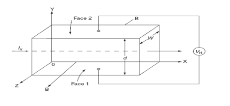
11 Figure: Hall Effect
Suppose if the semiconductor is n-type, then mostly the carriers are electrons and the electric current is due to the drifting of electrons along negative X-direction or if the semiconductor is p-type, then mostly the carriers are holes and the electric current is due to drifting of the holes along positive X-direction.
As these carriers are moving in magnetic field in the semiconductor that mean they experience Lorentz force represented by FL
FL =Bevd
Where vd is the drift velocity of the carriers. (already explained in previous section).
We can obtain the direction of this force by applying Fleming’s left-hand rule in electromagnetism.
Fleming’s left-hand rule can be explained as If we stretch the thumb, fore finger and middle finger in three perpendicular directions so that the fore finger is parallel to the magnetic field and the middle finger is parallel to the current direction, then thumb represents the direction of force on the current-carrying carriers.
So the Lorentz force is exerted on the carriers in the negative Y-direction. Due to Lorentz force, more and more carriers will be deposited at the bottom face (represented by face 1in figure) of the conductor.
The deposition of carriers at the bottom face is continued till the repulsive force due to accumulated charge balances the Lorentz force.
After some time of the applied voltage, both the forces become equal in magnitude and act in opposite direction, then the potential difference between the top and bottom faces is equal to Hall voltage and that can be measured.
At equilibrium, the Lorentz force on a carrier
FL = Bevd……………..(1)
And the Hall force
FH = eEH ……………..(2)
Where EH is the Hall electric field due to accumulated charge.
At equilibrium, FH = FL
EEH = Bevd
∴ EH = Bvd ……………..(3)
If ‘d’ is the distance between the upper and lower surfaces of the slab, then the Hall field
EH =  ……………..(4)
In n-type material, Jx = –nevd
vd= -  ……………..(5)
Where n is free electron concentration, substituting (5) in (3), we have
∴ EH = -B ……………..(6)
For a given semiconductor, the Hall field EH is proportional to the current density Jx and the intensity of magnetic field ‘B’ in the material.
i.e. EH ∝ JxB
(or) EH = RHJxB ……………..(7)
Where RH = Hall coefficient
Equations (6) and (7) are same so, we have
RHJxB =-B
RH = - = -
= - ……………..(8)
Where ρ is charge density
Similarly for p-type material
RH =  =
= ……………..(9)
Using Equations (8) and (9), carrier concentration can be determined.
Thus, the Hall coefficient is negative for n-type material. In n-type material, as more negative charge is deposited at the bottom surface, so the top face acquires positive polarity and the Hall field is along negative Y-direction. The polarity at the top and bottom faces can be measured by applying probes.
Similarly, in case of p-type material, more positive charge is deposited at the bottom surface. So, the top face acquires negative polarity and the Hall field is along positive Y-direction. Thus, the sign of Hall coefficient decides the nature of (n-type or p-type) material.
The Hall coefficient can be determined experimentally in the following way:
Multiplying Equation (7) with ‘d’, we have
EHd = VH = RHJxBd ……………..(10)
From (Figure 11) we know the current density Jx
Jx= 
Where W is width of the box. Then, Equation (10) becomes
VH = RH Bd = RH
RH =  ……………..(11)
Substituting the measured values of VH, Ix, B and W in Equation(11), RH is obtained. The polarity of VH will be opposite for n- and p-type semiconductors.
The mobility of charge carriers can be found by using the Hall effect, for example, the conductivity of electrons is
n= neμn
Or we can rewrite it as
μn =  =n RH……………..(12)
By using equation (11)
μn = n ……………..(13)
27Question: Discuss the application of Hall Effect?
Solution:
• Using magnetic flux leakage – In order to properly inspect items such as pipes or tubes, Hall Effect probes work with something called magnetic flux leakage. This is a way of testing such items, and being able to spot potential corrosion, erosion, or pitting. This is specifically used in steel items, and can give important information about lifespan or safety.
• Sensors to detect rotation speed – A Hall Effect probe can be used to in bicycle wheels, speedometers in the automotive world, electronic types of ignition systems, and gear teeth.
• Used to detected movement – You will often find a Hall Effect probe used in such items as Go-Kart controls, smart phones, paintball guns, or airsoft guns, as well as some GPS systems.
• Ferrite Toroid Hall Effect current transducers – This is mainly used in electronic compasses, making use of the magnetic field to show direction.
• Split-ring clamp-on sensors – These types of Hall Effect probes are used to test equipment without having to take the whole circuit board apart, e.g. Complex items.
• Analog multiplication – Anything which needs a power measurement, e.g. Sensing, and also used in small computers.
• General power measurement – Basically any device which needs to be tested for its power input can be done by a Hall Effect probe.
• Position and motion sensors – This is mainly used in a DC motor, often the brushless type.
• The automotive world – Hall Effect probes are used widely in the automotive world, especially in fuel injection and ignition. Wheel rotation sensors also use Hall Effect probes, e.g. For anti-lock braking.
- For determination of type of given semiconductor.
- For N-type, Hall coefficient RH= negative
- For P-type, Hall coefficient RH= Positive
- To determine carrier concentration n andp; that is n=p=1/e𝑅𝐻
- Determination of mobility of charge carriers μn =
 =n RH. Where 𝜎= electrical conductivity
 - To determine the sign of charge carriers whether the conductivity is due to electrons or holes.
Main Advantages of Using Hall Sensors
Why is a Hall Effect probe advantageous in all of these instances? Because the probes are not affected by outside influences, e.g. Water or dirt. They can also easily sense the measure the output they need when they are placed in the right position. On top of this, Hall Effect probes are safer, because the voltage never actually makes it directly to the sensor/probe. This makes this type of measurement overall so much safer than other methods.
As you can see, understanding how something is put in practice in the real world really helps you to understand it in real terms. The Hall Effect is certainly very common place these days, in much more methods and applications than we realize. While certainly very useful in the automation world, even basic items such as a compass make large use of this scientific approach.
28Question: Write a note on fullerene?
Solution:
FULLERENE
Carbon has many allotropes like diamond, graphite,etc. Third allotropic form of carbon is fullerene. Any molecule made of only carbon atoms is fullerene. These can be of any shape like ellipsoid, sphere or tube. Fullerenes having spherical geometry are called buckyballs.Cylindrical fullerenes are given the name nanotubes. Graphite has layered structure in which hexagonal rings are linked to each other. Fullerene structure is like graphitebut there may also be pentagonal rings in fullerene structure.
Richard Buckminster Fuller was an architect who designed a geodesic dome having shape like interconnected rings. As fullerene also has interlinked rings structure, so these are given the name Buckminsterfullerene (C60). After discovery of buckminsterfullerene, the fullerene family was discovered. The suffix “ene” tells that every carbon atom is bonded covalently to other three carbon atoms instead of four. It indicatesthat there are double bonds in fullerenes.
Any molecule having only carbon atoms in various shapes like hollow sphere, tube or ellipsoid is called as fullerene. Fullerenes have interconnected carbon atoms in hexagonal and pentagonal rings. Fullerenes have similar structure like graphite except these may have pentagonal rings. Figure 35 shows the structural configuration and atomic arrangement of three allotropes of carbon.
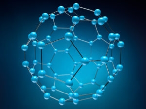
Figure 35
Types of Fullerene
Fullerenes were discovered in 1985. After that, various types of fullerenes were discovered on the basis of structural variations.
These are following:
Buckyball Clusters
The most common buckyball is C60but C20is the smallest member in buckyball clusters . Figure 36 shows the structure of smallest buckyball.
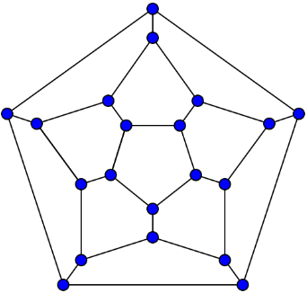
Figure 36:Structure of 20-Fullerene (Dodecahedral Graph).
Nanotubes
Nanotubes have very small dimensions. These are hollow from inside like a tube with single or multiple boundaries. Nanotubes are mostly used in electronic industries. Figure 37 shows structure of nanotube .
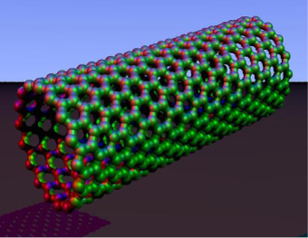
Figure 37: Structure of Nanotube.
Megatubes
Megatubes have larger diameter as compared to nanotubes. They have walls of various sizes. Megatubes are mainly used for the transportation of different sized molecules.
Polymers
Polymers are formed under high temperature and high pressure. These can have different structures like one dimensional chain, two-dimensional and three-dimensional shapes. Figure38 shows structure of polymers.

Figure 38 : Structure of Polymers
Nano-onions
Nano-onions are spherical in shape. They have multiple carbon layered structure with a buckyball core between the layers. Nano-onions are utilized as good lubricants. Figure39 shows the structure of nano-onions.
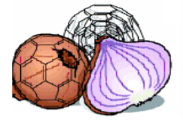
Figure 39: Structure of Nano-Onions.
Buckminsterfullerene (C60)
C60 is a molecule having 60 carbon atoms. These atoms are arranged in a cage like structure having 12 pentagons and 20 hexagons. The shape of C60is like a soccer ball. The black portions of soccer ball are pentagons and white are hexagons. If we put carbon atoms atall these 60 points, then we get structure of buckminsterfullerene. If we imagine that the C60 molecule has size of the order of soccer ball, then size of soccer ball will be equal to earth size. C60 molecule is the most symmetric molecule having symmetries like reflection symmetry, rotational symmetry etc. A geodesic dome has the similar structural view like a buckminsterfullerene as shown in Figure 40.
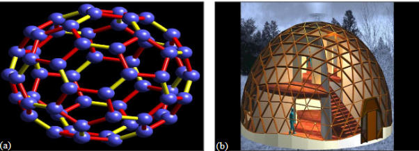
Figure 40: (a)A Buckminsterfullerene, (b) A Geodesic Dome.
Structure of C60
In C60, each carbon atom is covalently bonded to three neighbouring carbon atoms. Hence it has sp2 hybridization. Hybridization of carbon atoms in C60is shown in Figure 41Fullerenes have 20 hexagonal and 12 pentagonal rings. On every polygon’s vertices,there is a carbon atom and along edge of each polygon,there is a bond. It has two bond lengths and average bond length of C60is 1.4Å. C60is not super-aromatic. It is an alkene having electron deficiency property. It reacts with species which are rich of electrons. There can be an infinite number of fullerenes on the basis of number of pentagonal and hexagonal rings. C60has face center cubic lattice structure. The van-der Waals diameter andnucleus to nucleus diameter of this molecule are 1.1 and 0.71nm respectively.
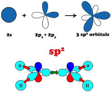
Figure 41
PROPERTIES
Fullerenes are chemically reactive and can be added to polymer structures to create new co-polymers with specific physical and mechanical properties. Their application as polymer transistors [Organic Field Effect Transistors (OFETS)] and photodetectors has also been increasing. Because their electrical resistance changes significantly when other molecules are attached to the carbon atoms, they can be used in developing sensors that can detect chemical vapours such as carbon monoxide or biological molecules.
Another property of medical interest is that they can easily penetrate membranes and cell walls and serve as drug delivery systems. Fullerenes are powerful antioxidants, reacting readily and at a high rate with free radicals, which are often the cause of cell damage or death. They behave like "radical sponges," as they can sponge-up and neutralize 20 or more free radicals per fullerene molecule. The most interesting property for medical use is their antioxidant activity and their sensing/detecting ability, and the most interesting potential application of fullerenes in nanopharmacology is the development of targeted drug delivery systems.
They called super-aromatics. They assigned to this class of compounds molecule of polyhedral form which contain electrons in molecular orbital delocalised on the surface of a three dimensional structure having an almost spherical symmetry. They suggested that C60 molecule has the structure of truncated icosahedron. This C60molecule possesses a system of mobile electron which contributes additional stabilisation to polyhedron as in benzene molecule. They produced the first quantitative estimates of resonance energy for this unusual type of conjugated molecule and concluded that C60cluster has great resonance energy than benzene molecule. Hence C60 molecule was assigned to a new class of aromatic system.