Unit – 3
Transistors
Q1) Determine the values of VCC RC and RB of a fixed bias configuration for a given load line and defined Q point.
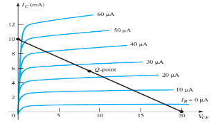
A1)
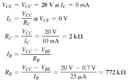
Q2) A npn silicon transistor has VCC = 6 V and the collector load RC = 2.5 kΩ. Find: (i) The maximum collector current that can be allowed during the application of signal for faithful amplification. (ii) The minimum zero signal collector current required.
A2)
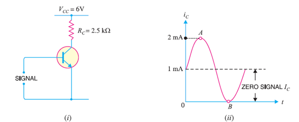
A2)
Collector supply voltage, VCC = 6 V
Collector load, RC = 2.5 kΩ
(i) We know that for faithful amplification, VCE should not be less than 1V for silicon transistor.
∴ Max. Voltage allowed across RC = 6 − 1 = 5 V
∴ Max. Allowed collector current = 5 V/RC = 5 V/2.5 kΩ = 2 mA
Thus, the maximum collector current allowed during any part of the signal is 2 mA. If the collector current is allowed to rise above this value, VCE will fall below 1 V. Consequently, value of β will fall, resulting in unfaithful amplification.
(ii) During the negative peak of the signal, collector current can at the most be allowed to become zero. As the negative and positive half cycles of the signal are equal, therefore, the change in collector current due to these will also be equal but in opposite direction.
∴ Minimum zero signal collector current required = 2 mA/2 = 1 mA
During the positive peak of the signal [point A in Fig. 1(ii)], iC = 1 + 1 = 2mA
And during the negative peak (point B), iC = 1 − 1 = 0 mA
Q3) A transistor employs a 4 kΩ load and VCC = 13V. What is the maximum input signal if β = 100? Given Vknee = 1V and a change of 1V in VBE causes a change of 5mA in collector current.
A3)
Collector supply voltage, VCC = 13 V
Knee voltage, Vknee = 1 V
Collector load, RC = 4 kΩ
∴ Max. Allowed voltage across RC = 13 − 1 = 12 V
∴ Max. Allowed collector current, iC =12 V /RC = 12 V/ 4 KΩ = 3 mA
Maximum base current, iB = iC / β = 3 mA / 100 = 30 μA
Now collector-current / Base voltage (signal voltage) = 5 mA/V
∴Base voltage (signal voltage) = Collector current / (5 mA/V) = 3 mA /(5 mA/V) = 600 mV
Q4) Fig. (i) shows biasing with base resistor method. (i) Determine the collector current IC and collector-emitter voltage VCE. Neglect small base-emitter voltage. Given that β = 50. (ii) If RB in this circuit is changed to 50 kΩ, find the new operating point.
A4)
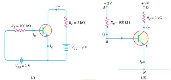
In the circuit shown in Fig. (i), biasing is provided by a battery VBB (= 2V) in the base circuit which is separate from the battery VCC (= 9V) used in the output circuit.
The same circuit is shown in a simplified way in Fig. (ii). Here, we need show only the supply voltages, + 2V and +9V. It may be noted that negative terminals of the power supplies are grounded to get a complete path of current.
IB RB + VBE = 2
IB = 20 A
A
IC =  IB = 50x20
 A= 1mA
IC RC + VCE = 9
VCE = 9- (1mA x 2000) = 7V
When RB is made equal to 50k
IC =  IB = 50x40
 A= 2mA
VCE = 9- (2mA x 2000) = 5V
So, the operating point is 5V and 2mA
Q5) Fig. (i) shows that a silicon transistor with β = 100 is biased by base resistor method. Draw the d.c. Load line and determine the operating point. What is the stability factor?
A5)
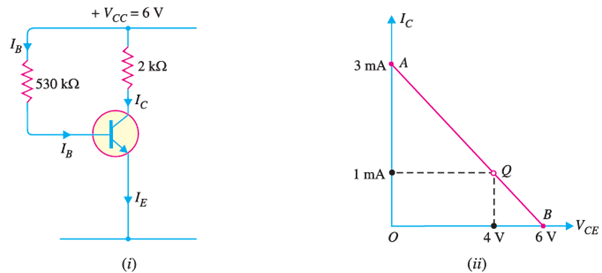
Here, VCC = 6 V, RB = 530 kΩ, RC = 2 kΩ
D.C. Load line
Referring to Fig. 3 (i), VCE = VCC − ICRC
When IC = 0,
VCE = VCC = 6 V. This locates the first point B (OB = 6V) of the load line on collector-emitter voltage axis as shown in Fig. (ii).
When VCE = 0,
IC = VCC/RC = 6V/2 kΩ = 3 mA.
This locates the second point A (OA = 3mA) of the load line on the collector current axis. By joining points A and B, d.c. Load line AB is constructed as shown in Fig. (ii).
Operating point Q
As it is a silicon transistor, therefore, VBE = 0.7V.
IB RB +VBE =VCC
IB = (6-0.7)/530x103 =10 A
A
IC =  IB = 100x10= 1mA
VCE = 6- (1mA x 2000) = 4V
The operating point is 4V, 1mA.
The stability factor is given by  +1 = 100+1 =101
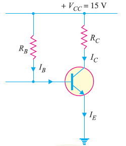
Q6) Design base resistor bias circuit for a CE amplifier such that operating point is VCE = 8V and IC = 2 mA. You are supplied with a fixed 15V d.c. supply and a silicon transistor with β = 100. Take base-emitter voltage VBE = 0.6V. Calculate also the value of load resistance that would be employed.
A6)
Fig. Shows CE amplifier using base resistor method of biasing.
A6)
VCC = 15v
β = 100
VBE = 0.6V
VCE = 8V, IC = 2 mA.
VCC = VCE + IC RC
15 = 8+ 2mAxRC
RC = 3.5k
IC =  IB
IB
IB = 2/100 =0.02mA
VCC = IB RB + VBE
RB = (15-0.6)/ (0.02x10⁻³) = 720k
Q7) In base bias method, how Q-point is affected by changes in VBE and ICBO.
A7)
In addition to being affected by change in β, the Q-point is also affected by changes in VBE and ICBO in the base bias method.
(i) Effect of VBE:
The base-emitter-voltage VBE decreases with the increase in temperature (and vice-versa). The expression for IB in base bias method is given by;
IB = VCC – VBE/RB
It is clear that decrease in VBE increases IB. This will shift the Q-point (IC = βIB and VCE = VCC – IC RC). The effect of change in VBE is negligible if VCC >> VBE (VCC at least 10 times greater than VBE).
(ii) Effect of ICBO:
The reverse leakage current ICBO has the effect of decreasing the net base current and thus increasing the base voltage. It is because the flow of ICBO creates a voltage drop across RB that adds to the base voltage as shown in Fig. 6. Therefore, change in ICBO shifts the Q-point of the base bias circuit.
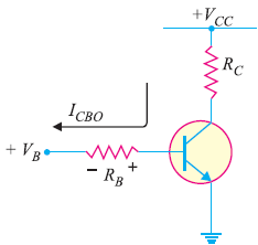
However, in modern transistors, ICBO is usually less than 100 nA and its effect on the bias is negligible if VBB >> ICBO RB.
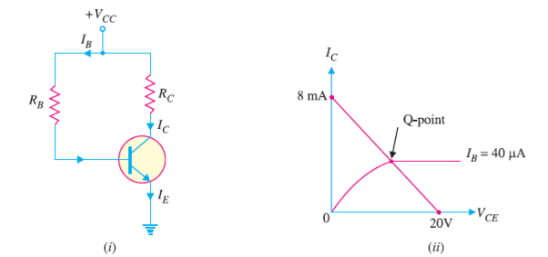
Q8) For figure below is a resistor transistor circuit. The device has the characteristics as shown below. Find VCC, RC and RB?
A8)
The DC Line voltage VCC = 20V
Maximum IC = VCC/RC
RC = 20/8x10-3=2.5k
IB = VCC – VBE/RB
RB = 20-0.7/40x10-6 = 482.5K
Q9) A 5.0V stabilized power supply is required to be produced from a 12V DC power supply input source. The maximum power rating PZ of the zener diode is 2W. Using the zener regulator circuit above calculate:
a). The maximum current flowing through the zener diode.
b). The minimum value of the series resistor, RS
c). The load current IL if a load resistor of 1kΩ is connected across the zener diode.
d). The zener current IZ at full load.
A9)
a). The maximum current flowing through the zener diode.
Maximum current = Watts/ Voltage =2W/5V =400mA
b). The minimum value of the series resistor, RS
 = 17.5 Ω
c). The load current IL if a load resistor of 1kΩ is connected across the zener diode.

d). The zener current IZ at full load.
Iz =Is -Il =440mA – 5mA = 395mA
Q10) In a CB IE= 2mA, IC=1.5mA. Calculate IB?
A10)
IE =IB+IC
2= IB+1.5
IB=0.5mA
Q11) In a CB current amplification factor is 0.9. If emitter current is 1.2mA. Determine the value of base current?
A11)
α = 0.9
IE =1.2mA
α = IC/ IE
IC = α IE =0.9 x 1.2 = 1.08mA
IE =IB+IC
1.2= IB+1.08
IB= 0.12mA
Q12) In a CB connection IC=1.0mA and IB= 0.02mA. Find the value of current amplification factor?
A12) IE =IB+IC =1+0.02 = 1.02mA
α = IC/ IE
α = 1.0/1.02 = 0.98
Q13) In a CB connection the emitter current is 0.98mA. If the emitter circuit is open the collector current becomes 40 A. Find total collector current. α =0.92
A13) ICBO=40 A
A
IC = α IE+ICBO
= (0.92 x 0.98x10-3) + 40x10-6
IC =0.94mA
Q14) In a common base connection, α = 0.95. The voltage drop across 3 kΩ resistance which is connected in the collector is 2.5 V. Find the base current.
A14) IC = 2.5/3000 = 0.83mA
α = IC/ IE
IE = IC/α =0.83/0.95=0.87mA
IE =IB+IC
0.87 =IB+0.83
IB=0.04mA
Q15) Find the value of β if (i) α = 0.9 (ii) α = 0.98 (iii) α = 0.99.
A15)
 = α/1- α = 0.9/1-0.9 = 9
 = α/1- α = 0.98/1-0.98 = 49
 = α/1- α = 0.99/1-0.99 = 99
Q16) The collector leakage current in a transistor is 200 μA in CE arrangement. If now the transistor is connected in CB arrangement, what will be the leakage current? Given that β = 120.
A16) ICEO=200 μA
 = 120
= 120
α = /1+
/1+ = 120/121=0.99
ICEO=ICBO/1- α
ICBO= 1.6 μA
Q17) For a certain transistor, IB = 18 μA; IC = 2 mA and β = 60. Calculate ICBO.
A17)
IC =  IB+ICEO
ICEO= IC -  IB= 2x10⁻³-(60x18x10-6) = 0.92mA
α = /1+
/1+ = 60/61=0.98
ICBO= (1- α) ICEO = (1-0.98)x 0.92=15.08 μA
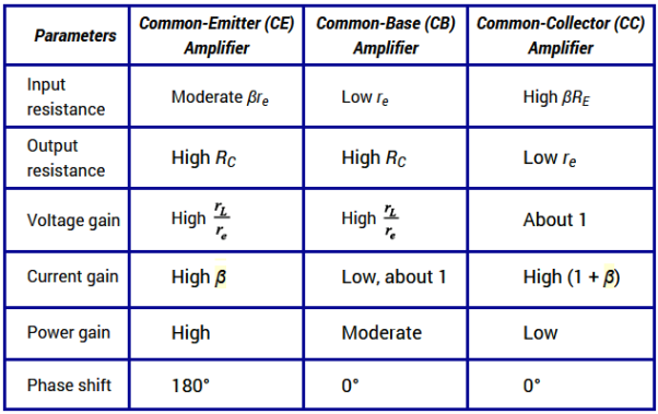
Q18) Compare CB CE and CC configuration?
A18)
Q19) Draw and explain input and output characteristics of CB configuration?
A19)
Input Characteristic Curve
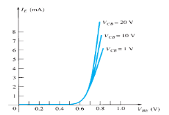
Fig: Input Characteristic Curve
- It is the relation between the input current IE to the input voltage VBE for various levels of output voltage VCB.
- It is also known as driving point characteristics.
Output Characteristic Curve
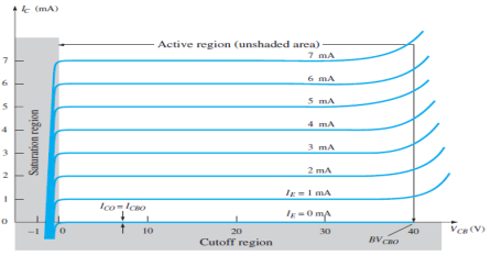
Fig: Output Characteristic Curve
- It is the relation between the output current IC to the output voltage VCB for various levels of input current IE.
- It is also known as collector set of characteristics.
- It has three basic regions:
- Active Region
Here, base-emitter junction is forward biased and collector-base junction is reverse biased.
As input current IE increases above zero, output current IC increases to a magnitude equal to IE as determined by the basic transistor current relationship.
So, the first approximation determined by the curve is
IC ≈ IE
2. Cut-off Region
It is defined as the region where the collector current IC is equal to 0A.
Here, the base-emitter junction and the collector-base junction both are in reverse bias.
3. Saturation Region
It is the region that lies towards the left of VCB = 0V.
Here, the base-emitter junction and the collector-base junction both are in forward bias.
Q20) Explain difference between avalanche and Zener breakdown?
A20)
Zener Breakdown | Avalanche Breakdown |
The process in which the electrons move across the barrier from the valence bond of p-type material to the conduction band of n-type material is known as Zener diode | The process of applying high voltage and increasing the free electrons or electric current in semiconductors and insulating materials is called an avalanche breakdown. |
This is observed in Zener diodes having a Zener breakdown voltage  | This is observed in Zener diode having a Zener breakdown voltage  |
The valence electrons are pulled into conduction due to the high electric field in the narrow depletion region. | The valence electrons are pushed to conduction due to the energy imparted by accelerated electrons, which gain their velocity due to their collision with other atoms. |
The increase in temperature decreases the breakdown voltage | The increase in temperature increase the breakdown voltage. |
The VI characteristic of a Zener breakdown has a sharp curve. | The VI characteristic curve of the avalanche breakdown is not as sharp as the Zener breakdown. |
It occurs in diodes that are highly doped | It occurs in diodes that are lightly doped. |
Q21) The MOSFET circuit shown below uses a MOSFET with the indicated characteristics. For each of the cases listed, solve MOSFET’s device current and drain voltage, and indicate whether the device is operating in saturation or triode. Given Kn = 250µA/ V2 VThN = 0.5V
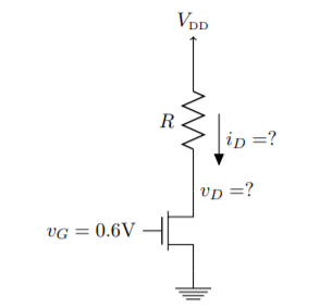
(A) R = 100Ω (B) R = 1kΩ (C) R = 10kΩ?
A21)
If the device is in saturation, then the device’s current and drain voltage are:

Where vOV = vG − VTh = 0.1 V. If the device is in triode, then the solution is more complex:
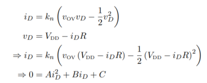
Since the triode solution is more complex, it’s easier to first assume saturation and see if the result is consistent with that assumption. In saturation, the device current should always be 2.5 µA.
(A) R = 100Ω — In this case, we find

This result is consistent with being in saturation since vD > vOV.
(B) R = 1kΩ — In this case, we find

This result is consistent with being in saturation since vD > vOV.
(C) R = 10kΩ— In this case, we find

This result is consistent with being in saturation since vD > vOV.
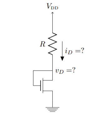
Q22) The MOSFET circuit shown below uses a MOSFET with the indicated characteristics. For each of the cases listed, solve MOSFET’s device current and drain voltage, and indicate whether the device is operating in saturation or triode. Kn = 250µA/ V2 VThN = 0.5V
(A) R = 100Ω (B) R = 1kΩ (C) R = 10kΩ
A22)
In this problem, the device is always in saturation due the diode connection, which guarantees vDS > vOV in all cases. The solution requires solving a quadratic
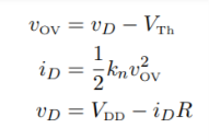
It is perhaps quickest to solve for vOV:
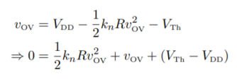
Now we can use the quadratic formula to solve


In the numerator, we choose ‘+’ from the ‘±’ in order to obtain a positive-valued solution (a negative valued solution doesn’t make physical sense).
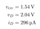
(A) R = 100Ω — In this case, we find

(B) R = 1kΩ — In this case, we find
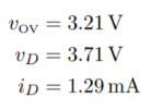
(C) R = 10kΩ — In this case, we find
Q23) The MOSFET circuit shown below uses a MOSFET with the indicated characteristics. For each of the cases listed, solve MOSFET’s device current and drain voltage, and indicate whether the device is operating in saturation or triode. Kn = 250µA/ V2 VThN = 0.5V. (A) R = 100Ω (B) R = 1kΩ (C) R = 10kΩ
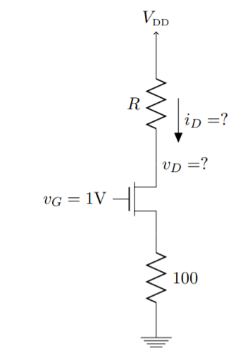
A23)
In this problem, we can use the same procedure from Problem 1. Since RS is small, it should have a minor effect on the DC solution. We can evaluate that effect by iterating as follows:
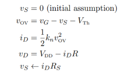
If we initially assume vS = 0, then we can solve for a new vS, then repeat the equations until the results stabilizes. From this procedure, we find the following

As long as the device stays in saturation, these results should not depend on R and will be the same for each case. Then the solutions are:
(A) R = 100Ω
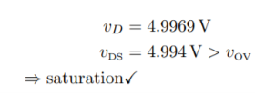
(B) R = 1kΩ:

(C) R = 10kΩ

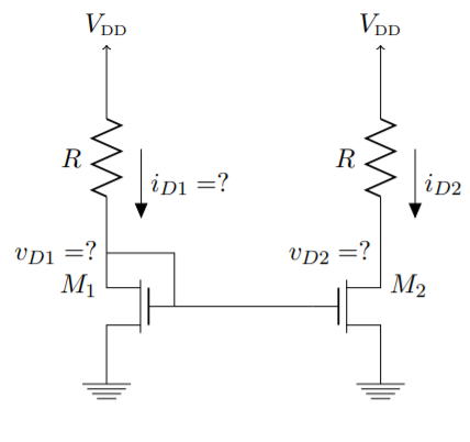
Q24) The MOSFET circuit shown below uses a pair of identical MOSFETs with the indicated characteristics. For each of the cases listed, solve MOSFETs’ device currents and drain voltages, and indicate whether each device is operating in saturation or triode. Kn = 250µA/ V2, VThN = 0.5V. (A) R = 100Ω (B) R = 1kΩ (C) R = 10kΩ.
A24)
Notice that the left-hand side of this circuit is identical to the one in Problem 2. The solution should be exactly the same. On the right hand side, there is an identical MOSFET and an identical resistor. Furthermore, the two MOSFETs share identical gate and source voltages, and should therefore have identical currents (iD2 = iD1 in all cases). With all other things being equal, the only remaining unknown (vD2) should also be identical to its twin on the right-hand side. This is called a symmetry argument, and is a very useful method for analyzing current mirrors and differential circuits.