Unit - 5
Input-Output Organization
Q1) What is a priority interrupt?
A1) The CPU initiates data flow between the CPU and the peripherals. The CPU, on the other hand, cannot begin the transfer until the peripheral is ready to communicate with it. An interrupt signal is generated when a device is ready to connect with the CPU. The computer is connected to a variety of input-output devices, each of which can issue an interrupt request.
The interrupt system's primary function is to locate the source of the interruption. It's also possible that multiple devices will require CPU communication at the same time. The interrupt system must then determine which device should be serviced first.
A priority interrupt is a mechanism that determines the order in which the CPU will serve multiple devices that issue interrupt signals at the same time. While another interrupt is being handled, the system has the authority to decide which conditions are authorized to interrupt the CPU. Devices that transfer data quickly, such as magnetic drives, are given high priority, whereas slower devices, such as keyboards, are given low priority.
When two or more devices interrupt the computer at the same time, the computer prioritizes the higher-priority device.
Q2) What are the types of interrupt?
A2) Types of interrupt
Types of Interrupts:
The following are some examples of interrupts:
Hardware Interrupts
When the CPU receives a signal from an external device or hardware, it is referred to as a hardware interrupt.
Consider the following scenario: when we press a key on our keyboard to conduct an operation, the key will generate an interrupt signal, causing the CPU to perform the action. There are two types of interruptions:
Maskable Interrupt
When a significantly higher priority interrupt occurs at the same moment, hardware interrupts can be delayed.
Non - Maskable Interrupt
Hardware interrupts that cannot be delayed and must be handled instantly by the processor.
Software Interrupts
A software interrupt is a computer system interrupt that is caused by any internal mechanism of the computer system. There are two types of it:
Normal Interrupt
Normal software interrupts are the ones that are caused by software instructions.
Exception
Exceptions are unplanned interruptions that occur during the execution of a program, such as division by zero.
Daisy Chaining Priority
This method of determining interrupt priority entails connecting all devices that emit interrupt signals in a serial fashion. The device with the highest priority is placed first, followed by devices with lower priorities, and finally the device with the lowest priority is placed last in the chain.
All of the devices in a daisy chaining system are connected in a serial fashion. All devices must respond to the interrupt line request. If any device has a low-level interrupt signal, the interrupt line goes low-level and the interrupt input in the CPU is enabled. The interrupt line remains in a high level state when there is no interrupt. The interrupt acknowledge line is enabled by the CPU in response to the interrupt. The gadget 1 receives this signal at its PI input. Only if device 1 does not seek an interrupt does the acknowledge signal flow to the next device through the PO output.
The block diagram for a daisy chaining priority system is shown in the diagram below.
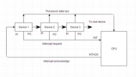
Fig 1: Block diagram of daisy chaining priority
Q3) What is a peripheral device?
A3) Peripheral device
The Input / output organization of computer depends upon the size of computer and the peripherals connected to it. The I/O Subsystem of the computer, provides an efficient mode of communication between the central system and the outside environment.
There are three types of peripherals:
- Input peripherals: Allows user input, from the outside world to the computer. Example: Keyboard, Mouse etc.
- Output peripherals: Allows information output, from the computer to the outside world. Example: Printer, Monitor etc
- Input-Output peripherals: Allows both input(from outside world to computer) as well as, output(from computer to the outside world). Example: Touch screen etc.
Q4) Write the difference between peripheral device and CPU?
A4) The Major Differences between peripheral devices and CPU:
1. Peripherals are electro mechanical and electromagnetic devices and CPU and memory are electronic devices. Therefore, a conversion of signal values may be needed.
2. The data transfer rate of peripherals is usually slower than the transfer rate of CPU and consequently, a synchronization mechanism may be needed.
3. Data codes and formats in the peripherals differ from the word format in the CPU and memory.
4. The operating modes of peripherals are different from each other and must be controlled so as not to disturb the operation of other peripherals connected to the CPU.
To resolve these differences, computer systems include special hardware components between the CPU and Peripherals to supervises and synchronizes all input and out transfers. These components are called Interface Units because they interface between the processor bus and the peripheral devices.
Q5) What do you mean by input output interface?
A5) Input Output interface
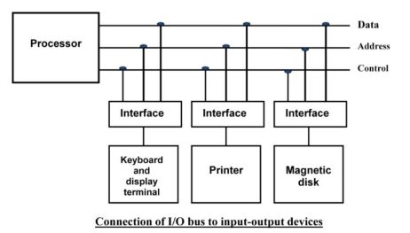
Peripherals connected to a computer need special communication links for interfacing with CPU. In computer system, there are special hardware components between the CPU and peripherals to control or manage the input-output transfers.
These components are called input-output interface units because they provide communication links between processor bus and peripherals. They provide a method for transferring information between internal system and input-output devices.
Q6) Explain data transfer scheme?
A6) Data transfer scheme
Data transfer between the central unit and I/O devices can be accomplished in one of three ways, as shown below:
● Programmed I/O
● Interrupt Initiated I/O
● Direct Memory Access
Programmed I/O
I/O instructions written in a computer program result in programmed I/O instructions. The program's instruction triggers the transfer of each data item.
Typically, the software is in charge of data transport between the CPU and peripherals. Transferring data with programmed I/O necessitates the CPU's ongoing supervision of the peripherals.
Interrupt initiated I/O
The CPU remains in the program loop in the programmed I/O approach until the I/O unit indicates that it is ready for data transfer. This is a time-consuming procedure because it wastes the processor's time.
Interrupt started I/O can be used to solve this problem. The interface creates an interrupt when it determines that the peripheral is ready for data transfer. When the CPU receives an interrupt signal, it stops what it's doing and handles the I/O transfer before returning to its prior processing activity.
Direct Memory Access
The speed of transmission would be improved by removing the CPU from the path and allowing the peripheral device to operate the memory buses directly. This technique is known as DMA.
The interface transfers data to and from the memory via the memory bus in this case. A DMA controller is responsible for data transport between peripherals and the memory unit.
DMA is used by many hardware systems, including disk drive controllers, graphics cards, network cards, and sound cards, among others. In multicore CPUs, it's also used for intra-chip data transport. In DMA, the CPU would start the transfer, perform other tasks while it was running, and then get an interrupt from the DMA controller when the transfer was finished.
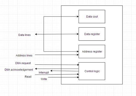
Fig 2: DMA
Q7) Describe program control?
A7) Computer instructions are always stored in sequential memory locations. For processing and execution, these instructions are fetched from different memory regions.
The program counter is advanced by one when an instruction is fetched from memory, pointing to the address of the next successive instruction in the memory. The program control, together with the program counter, which carries the location of the next instruction to be fetched, is returned to the fetch cycle once a data transfer and data manipulation instruction has been executed.
The program control instructions provide the criteria that can change the content of the program counter, whereas the data transfer and manipulation instructions specify the conditions for data processing operations.
An interrupt/break in the execution of instructions can be caused by a change in the content of the program counter. The program control instructions, on the other hand, control the flow of program execution and can branch to different program segments.
The table below lists some of the program control instructions.
Program Control Instructions
Name | Mnemonics |
Branch | BR |
Jump | JMP |
Skip | SKP |
Call | Call |
Return | RET |
Compare (by Subtraction) | CMP |
Test (by ANDing) | TST |
The instruction is a one-address branch. It's written as BR ADR, where ADR stands for address mnemonic. The value of ADR is transferred into the program counter by the branch instruction. The terms "branch" and "leap" are used interchangeably to describe the same thing. However, they can also refer to different addressing modes.
The condition to move the flow of execution is specified by conditional branch instructions such as 'branch if positive' or 'branch if zero.' The branch address is loaded into the program counter when the condition is met.
The conditional branch instructions are shown in the diagram.
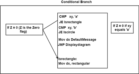
Fig 3: Conditional branch instruction
Arithmetic subtraction is performed through the compare command. The operation's outcome is not recorded here; instead, the status bit conditions are set. The test instruction modifies the status bits by performing a logical AND operation on two operands.
Q8) Define interrupt?
A8) Interrupt is a signal emitted by hardware or software when a process or an event needs immediate attention. It alerts the processor to a high priority process requiring interruption of the current working process. In I/O devices one of the bus control lines is dedicated for this purpose and is called the Interrupt Service Routine (ISR).
When a device raises an interrupt at let’s say process i, the processor first completes the execution of instruction i. Then it loads the Program Counter (PC) with the address of the first instruction of the ISR. Before loading the Program Counter with the address, the address of the interrupted instruction is moved to a temporary location. Therefore, after handling the interrupt the processor can continue with process i+1.
While the processor is handling the interrupts, it must inform the device that its request has been recognized so that it stops sending the interrupt request signal. Also, saving the registers so that the interrupted process can be restored in the future, increases the delay between the time an interrupt is received and the start of the execution of the ISR. This is called Interrupt Latency.
Hardware Interrupts:
In a hardware interrupt, all the devices are connected to the Interrupt Request Line. A single request line is used for all the n devices. To request an interrupt, a device closes its associated switch. When a device requests an interrupt, the value of INTR is the logical OR of the requests from individual devices.
Sequence of events involved in handling an IRQ:
- Devices raise an IRQ.
- Processor interrupts the program currently being executed.
- Device is informed that its request has been recognized and the device deactivates the request signal.
- The requested action is performed.
- Interrupt is enabled and the interrupted program is resumed.
Handling Multiple Devices:
When more than one device raises an interrupt request signal, then additional information is needed to decide which device to be considered first. The following methods are used to decide which device to select: Polling, Vectored Interrupts, and Interrupt Nesting. These are explained as following below.
1. Polling:
In polling, the first device encountered with IRQ bit set is the device that is to be serviced first. Appropriate ISR is called to service the same. It is easy to implement but a lot of time is wasted by interrogating the IRQ bit of all devices.
2. Vectored Interrupts:
In vectored interrupts, a device requesting an interrupt identifies itself directly by sending a special code to the processor over the bus. This enables the processor to identify the device that generated the interrupt. The special code can be the starting address of the ISR or where the ISR is located in memory, and is called the interrupt vector.
3. Interrupt Nesting:
In this method, I/O device is organized in a priority structure. Therefore, interrupt request from a higher priority device is recognized where as request from a lower priority device is not. To implement this each process/device (even the processor). Processor accepts interrupts only from devices/processes having priority more than it.
Processors priority is encoded in a few bits of PS (Process Status register). It can be changed by program instructions that write into the PS. Processor is in supervised mode only while executing OS routines. It switches to user mode before executing application programs.
Q9) Describe data memory access transfer?
A9) The microcomputer system basically consists of three blocks
● The microprocessor
● The memories of microprocessor like EPROM and RAM
● The I/O ports by which they are connected.
The possible data transfers are indicated below.
● Between the memory and microprocessor data transfer occurs by using the LDA and STA instructions.
● Between microprocessor and I/O ports also data transfer occurs by the help of two instructions IN and OUT.
● Through DMA data transfer, data is transferred between the Input Output ports and the memory.
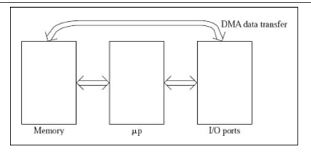
Fig 4: The figure shows possible ways of data transfers in a microcomputer system.
For performing the data transfer either between the microprocessor and memory or between I/O ports and the processor instructions for the programs are executed such that, the data transfers which are called as programmed data transfer, are already in used when a small amount of data transfer is involved in the process.
Both the microprocessor and the memory are made of semiconductor chips that work in comparable to electronic speeds. So it is not all a problem to transfer the data between microprocessor and memory. If the case arises such that the memory is slow than the microprocessor, the processor used has to insert wait states. No problem other than this can occur.
The ports like 8255, 8212 and others are also made by semiconductor chips which work at electronic speeds. We use them for interfacing the INPUT–OUTPUT devices which are electromechanical in nature, and hence the speed of the microprocessor turns slower which results the transfer of data between microprocessor and INPUT-OUTPUT ports becomes very complex in nature.
If the data transfer which is used for reading from the memory location is 3456H and then writing to output port number is 50H which takes 13 clocks only for reading from memory location 3456H using the LDA 3456H instruction and ten clocks for writing to the output port number 50H. Therefore 23 clocks in total. If the processor works at an internal frequency of 3-MHz with a clock period of 0.33μs, it takes a fraction of 7.66μs to work externally. By using the program data transfer scheme, input port 40H is read and written to the memory location input port 2345H
If we use DMA data transfer to read from memory location 3456H and write to the output port number 50H only four clocks are needed, which results a fraction of only 1.33μs. Some devices like hard disk and floppy disk can perform data transfer at a very fast speed. A floppy disk of memory 1.44 MB which rotates at a speed of 360 rpm, having 18 sectors per track, can store up to 512 bytes of memory, when the rate of data transfer becomes 54K bytes in a second, or about 19μs per byte. Hard disks can easily transfer data at least ten times faster. Hence it turns out to be 1.9μs per byte. This is the situation when DMA data transfer becomes compulsory. In the programmed data transfer process where we need 7.66μs per byte only the 4 bytes comes out from the hard disk in the same time repeatedly. Hence it can be concluded that I/O devices plays an important role in the DMA data transfer process.
To obtain statistics like average, the largest, and the smallest values, we use Analog to Digital converter. Using the programmed data transfer scheme 1,000 × 7.66 = 7,660μs of processor time is needed. But surprisingly using the DMA data transfer scheme only 1,000 × 1.33 = 1,330μs of time is needed. So when large amount of data is to be transferred between the memory and I/O port by routing each byte through microprocessor, it takes a lot of time, so to do the work in less time the I/O port can be directly accessed to the memory for data transfer. This scheme is termed as DMA data transfer.
Q10) What is input output processor?
A10) A processor having direct memory access is known as an input-output processor (IOP). The computer system is divided into memory units and processors in this way.
The input-output tasks are controlled and managed by each IOP. The IOP is comparable to the CPU, except that it only handles I/O processing details. The IOP is capable of retrieving and executing its own instructions. Only I/O transfers are managed using these IOP commands.
A block diagram of a computer with various I/O Processors is shown below. The memory unit is in the middle and can communicate with all of the processors.
The CPU is in charge of processing the data needed to complete the computations. The IOP acts as a conduit for data flow between peripherals and memory. The CPU is in charge of launching the I/O application.
IOPs work independently of the CPU, transferring data between peripherals and memory.
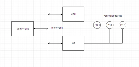
Fig 5: I/O processor
The IOP and the devices communicate in a manner similar to the program control way of data transfer. And the memory communication is comparable to that of direct memory access.
Each CPU in a huge computer is independent of the others, and any processor can start the operation.
The CPU can play the role of master processor while the IOP plays the role of slave processor. The CPU is in charge of beginning activities, but it is the IOP, not the CPU, who executes the commands. CPU instructions are used to initiate an I/O transfer. The IOP uses an interrupt to request CPU.
To distinguish them from instructions read by the CPU, instructions read from memory by an IOP are also referred to as commands. Programmers create commands, which are then stored in memory. The program for IOP is made up of command words. The CPU tells the IOP where to look in memory for commands.
Q11) Describe memory units?
A11) Semiconductor memory is used in any electronics assembly that uses computer processing technology. Semiconductor memory is the essential electronics component needed for any computer-based PCB assembly.
In addition to this, memory cards have become commonplace items for temporarily storing data - everything from the portable flash memory cards used for transferring files, to semiconductor memory cards used in cameras, mobile phones and the like.
The use of semiconductor memory has grown, and the size of these memory cards has increased as the need for larger and larger amounts of storage is needed.
To meet the growing needs for semiconductor memory, there are many types and technologies that are used. As the demand grows new memory technologies are being introduced and the existing types and technologies are being further developed.
A variety of different memory technologies are available - each one suited to different applications. Names such as ROM, RAM, EPROM, EEPROM, Flash memory, DRAM, SRAM, SDRAM, as well as F-RAM and MRAM are available, and new types are being developed to enable improved performance.
Terms like DDR3, DDR4, DDR5 and many more are seen and these refer to different types of SDRAM semiconductor memory.
In addition to this the semiconductor devices are available in many forms - ICs for printed board assembly, USB memory cards, Compact Flash cards, SD memory cards and even solid-state hard drives. Semiconductor memory is even incorporated into many microprocessor chips as on-board memory.
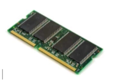
Fig 6: Printed circuit board containing computer memory
Semiconductor memory: main types
There are two main types or categories that can be used for semiconductor technology. These memory types or categories differentiate the memory to the way in which it operates:
RAM - Random Access Memory: As the names suggest, the RAM or random-access memory is a form of semiconductor memory technology that is used for reading and writing data in any order - in other words as it is required by the processor. It is used for such applications as the computer or processor memory where variables and other stored and are required on a random basis. Data is stored and read many times to and from this type of memory.
Random access memory is used in huge quantities in computer applications as current day computing and processing technology requires large amounts of memory to enable them to handle the memory hungry applications used today. Many types of RAM including SDRAM with its DDR3, DDR4, and soon DDR5 variants are used in huge quantities.
ROM - Read Only Memory: A ROM is a form of semiconductor memory technology used where the data is written once and then not changed. In view of this it is used where data needs to be stored permanently, even when the power is removed - many memory technologies lose the data once the power is removed.
As a result, this type of semiconductor memory technology is widely used for storing programs and data that must survive when a computer or processor is powered down. For example, the BIOS of a computer will be stored in ROM. As the name implies, data cannot be easily written to ROM. Depending on the technology used in the ROM, writing the data into the ROM initially may require special hardware. Although it is often possible to change the data, this gain requires special hardware to erase the data ready for new data to be written in.
As can be seen, these two types of memory are very different, and as a result they are used in very different ways.
Each of the semiconductor memory technologies outlined below falls into one of these two types of category. Each technology offers its own advantages and is used in a particular way, or for a particular application.
Q12) Describe semiconductor memory technology?
A12) Semiconductor memory technologies
There is a large variety of types of ROM and RAM that are available. Often the overall name for the memory technology includes the initials RAM or ROM and this gives a guide as to the overall type of format for the memory.
With technology moving forwards apace, not only are the established technologies moving forwards with SDRAM technology moving from DDR3 to DDR4 and then to DDR5, but Flash memory used in memory cards is also developing as are the other technologies.
In addition to this, new memory technologies are arriving on the scene and they are starting to make an impact in the market, enabling processor circuits to perform more effectively.
The different memory types or memory technologies are detailed below:
DRAM: Dynamic RAM is a form of random-access memory. DRAM uses a capacitor to store each bit of data, and the level of charge on each capacitor determines whether that bit is a logical 1 or 0. However these capacitors do not hold their charge indefinitely, and therefore the data needs to be refreshed periodically. As a result of this dynamic refreshing, it gains its name of being a dynamic RAM. DRAM is the form of semiconductor memory that is often used in equipment including personal computers and workstations where it forms the main RAM for the computer. The semiconductor devices are normally available as integrated circuits for use in PCB assembly in the form of surface mount devices or less frequently now as leaded components.
EEPROM: This is an Electrically Erasable Programmable Read Only Memory. Data can be written to these semiconductor devices and it can be erased using an electrical voltage. This is typically applied to an erase pin on the chip. Like other types of PROM, EEPROM retains the contents of the memory even when the power is turned off. Also, like other types of ROM, EEPROM is not as fast as RAM.
EPROM: This is an Erasable Programmable Read Only Memory. These semiconductor devices can be programmed and then erased at a later time. This is normally achieved by exposing the semiconductor device itself to ultraviolet light. To enable this to happen there is a circular window in the package of the EPROM to enable the light to reach the silicon of the device. When the PROM is in use, this window is normally covered by a label, especially when the data may need to be preserved for an extended period. The PROM stores its data as a charge on a capacitor. There is a charge storage capacitor for each cell and this can be read repeatedly as required. However, it is found that after many years the charge may leak away and the data may be lost. Nevertheless, this type of semiconductor memory used to be widely used in applications where a form of ROM was required, but where the data needed to be changed periodically, as in a development environment, or where quantities were low.
Flash memory: Flash memory may be considered as a development of EEPROM technology. Data can be written to it and it can be erased, although only in blocks, but data can be read on an individual cell basis.
To erase and re-programme areas of the chip, programming voltages at levels that are available within electronic equipment are used. It is also non-volatile, and this makes it particularly useful. As a result, Flash memory is widely used in many applications including USB memory sticks, compact Flash memory cards, SD memory cards and also now solid-state hard drives for computers and many other applications.
F-RAM: Ferroelectric RAM is a random-access memory technology that has many similarities to the standard DRAM technology. The major difference is that it incorporates a ferroelectric layer instead of the more usual dielectric layer and this provides its non-volatile capability. As it offers a non-volatile capability, F-RAM is a direct competitor to Flash.
MRAM: This is Magneto-resistive RAM, or Magnetic RAM. It is a non-volatile RAM memory technology that uses magnetic charges to store data instead of electric charges.
Unlike technologies including DRAM, which require a constant flow of electricity to maintain the integrity of the data, MRAM retains data even when the power is removed. An additional advantage is that it only requires low power for active operation. As a result, this technology could become a major player in the electronics industry now that production processes have been developed to enable it to be produced.
P-RAM / PCM: This type of semiconductor memory is known as Phase change Random Access Memory, P-RAM or just Phase Change memory, PCM. It is based around a phenomenon where a form of chalcogenide glass changes is state or phase between an amorphous state (high resistance) and a polycrystalline state (low resistance). It is possible to detect the state of an individual cell and hence use this for data storage. Currently this type of memory has not been widely commercialised, but it is expected to be a competitor for flash memory.
PROM: This stands for Programmable Read Only Memory. It is a semiconductor memory which can only have data written to it once - the data written to it is permanent. These memories are bought in a blank format and they are programmed using a special PROM programmer.
Typically, a PROM will consist of an array of fusible links some of which are "blown" during the programming process to provide the required data pattern.
SDRAM: Synchronous DRAM. This form of semiconductor memory can run at faster speeds than conventional DRAM. It is synchronised to the clock of the processor and is capable of keeping two sets of memory addresses open simultaneously. By transferring data alternately from one set of addresses, and then the other, SDRAM cuts down on the delays associated with non-synchronous RAM, which must close one address bank before opening the next.
Within the SDRAM family there are several types of memory technologies that are seen. These are referred to by the letters DDR - Double Data Rate. DDR4 is currently the latest technology, but this is soon to be followed by DDR5 which will offer some significant improvements in performance.
SRAM: Static Random-Access Memory. This form of semiconductor memory gains its name from the fact that, unlike DRAM, the data does not need to be refreshed dynamically.
These semiconductor devices are able to support faster read and write times than DRAM (typically 10 ns against 60 ns for DRAM), and in addition its cycle time is much shorter because it does not need to pause between accesses. However, they consume more power, they are less dense and more expensive than DRAM. As a result of this SRAM is normally used for caches, while DRAM is used as the main semiconductor memory technology.
Semiconductor memory technology is developing at a fast rate to meet the ever-growing needs of the electronics industry. Not only are the existing technologies themselves being developed, but considerable amounts of research are being invested in new types of semiconductor memory technology.
In terms of the memory technologies currently in use, SDRAM versions like DDR4 are being further developed to provide DDR5 which will offer significant performance improvements. In time, DDR5 will be developed to provide the next generation of SDRAM.
Other forms of memory are seen around the home in the form of USB memory sticks, Compact Flash, CF cards or SD memory cards for cameras and other applications as well as solid state hard drives for computers.
The semiconductor devices are available in a wide range of formats to meet the differing PCB assembly and other needs.
Q13) Explain memory hierarchy?
A13) A memory unit is the collection of storage units or devices together. The memory unit stores the binary information in the form of bits.
Memory Hierarchy is an enhancement to organize the memory such that it can minimize the access time. The Memory Hierarchy was developed based on a program behaviour known as locality of references.
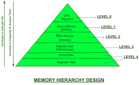
Fig 7: Memory hierarchy design
Memory Hierarchy is divided into 2 main types:
1. External Memory or Secondary Memory –
Comprising of Magnetic Disk, Optical Disk, Magnetic Tape i.e. peripheral storage devices which are accessible by the processor via I/O Module.
2. Internal Memory or Primary Memory –
Comprising of Main Memory, Cache Memory & CPU registers. This is directly accessible by the processor.
Memory Access Methods:
Each Memory is a collection of numerous memory locations. To access data from any memory, first it must be located and then the data is read from the memory location.
Access Methods in Memory:
- Random Access: Main memories are random access memories, in which each memory location has a unique address. Using this unique address any memory location can be reached in the same amount of time in any order.
- Sequential Access: This method allows memory access in a sequence or in order.
- Direct Access: In this mode, information is stored in tracks, with each track having a separate read/write head.
Levels of memory:
● Level 1 or Register.
It is a type of memory in which data is stored and accepted that are immediately stored in CPU. Most commonly used register is accumulator, Program counter, address register etc.
● Level 2 or Cache memory.
It is the fastest memory which has faster access time where data is temporarily stored for faster access.
● Level 3 or Main Memory.
It is memory on which computer works currently. It is small in size and once power is off data no longer stays in this memory.
● Level 4 or Secondary Memory.
It is external memory which is not as fast as main memory but data stays permanently in this memory.
Q14) Compare processor and memory speed?
A14) Processor Vs Memory speed
The processor is a computer component that works. There are registers in it, which are areas that a processor may access fast. Processor registers often contain a modest amount of quick storage for loading data from the main memory. There, the data is used for arithmetic operations and machine instructions manipulate or test it. The data will then be returned to the main memory.
Processor registers are typically addressed by mechanisms rather than memory in computer architecture. In other circumstances, though, memory addresses may be assigned to the registers. As the main memory, modern CPUs use either static or dynamic RAM, with the latter typically accessed via one or more cache levels. Despite this, processor registers are usually found at the top of the memory hierarchy.
Multiplexing and demultiplexing circuitry in RAM connects data lines to designated storage for reading and writing entries. Regardless of the actual location of data within the memory, RAM devices allow data items to be read or written in almost the same amount of time. As a result, reaching target data in RAM is faster than reaching data on CDs, DVDs, HDDs, SSDs, and other storage media.
Q15) Explain cache memory?
A15) The data or contents of the main memory that are used frequently by the CPU are stored in the cache memory so that the processor can easily access that data in a shorter time. Whenever the CPU needs to access memory, it first checks the cache memory. If the data is not found in the cache memory, then the CPU moves into the main memory.
Cache memory is placed between the CPU and the main memory. The block diagram for a cache memory can be represented as:

Fig 8: Cache memory
The cache is the fastest component in the memory hierarchy and approaches the speed of CPU components.
The basic operation of cache memory is as follows:
- When the CPU needs to access memory, the cache is examined. If the word is found in the cache, it is read from the fast memory.
- If the word addressed by the CPU is not found in the cache, the main memory is accessed to read the word.
- A block of words one just accessed is then transferred from main memory to cache memory. The block size may vary from one word (the one just accessed) to about 16 words adjacent to the one just accessed.
- The performance of the cache memory is frequently measured in terms of a quantity called hit ratio.
- When the CPU refers to memory and finds the word in the cache, it is said to produce a hit.
- If the word is not found in the cache, it is in the main memory and it counts as a miss.
- The ratio of the number of hits divided by the total CPU references to memory (hits plus misses) is the hit ratio.
Cache Memory is a special very high-speed memory. It is used to speed up and synchronizing with a high-speed CPU. Cache memory is costlier than main memory or disk memory but economical than CPU registers. Cache memory is an extremely fast memory type that acts as a buffer between RAM and the CPU. It holds frequently requested data and instructions so that they are immediately available to the CPU when needed.
Cache memory is used to reduce the average time to access data from the Main memory. The cache is a smaller and faster memory that stores copies of the data from frequently used main memory locations. There are various independent caches in a CPU, which store instructions and data.

Fig 9: Memory
Levels of memory:
- Level 1 or Register –
It is a type of memory in which data is stored and accepted that are immediately stored in the CPU. The most commonly used register is accumulator, Program counter, address register, etc.
- Level 2 or Cache memory –
It is the fastest memory which has faster access time where data is temporarily stored for faster access.
- Level 3 or Main Memory –
It is the memory on which the computer works currently. It is small in size and once power is off data no longer stays in this memory.
- Level 4 or Secondary Memory –
It is external memory that is not as fast as main memory but data stays permanently in this memory.
Application of Cache Memory –
- Usually, the cache memory can store a reasonable number of blocks at any given time, but this number is small compared to the total number of blocks in the main memory.
- The correspondence between the main memory blocks and those in the cache is specified by a mapping function.
Q16) Write about associative memory?
A16) An associative memory can be considered as a memory unit whose stored data can be identified for access by the content of the data itself rather than by an address or memory location.
Associative memory is often referred to as Content Addressable Memory (CAM).
When a write operation is performed on associative memory, no address or memory location is given to the word. The memory itself is capable of finding an empty unused location to store the word.
On the other hand, when the word is to be read from an associative memory, the content of the word, or part of the word, is specified. The words which match the specified content are located by the memory and are marked for reading.
The following diagram shows the block representation of an Associative memory.
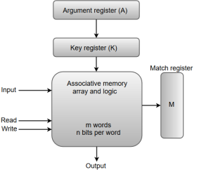
Fig 10 - Block representation of an Associative memory
From the block diagram, we can say that an associative memory consists of a memory array and logic for 'm' words with 'n' bits per word.
The functional registers like the argument register A and key register K each have n bits, one for each bit of a word. The match register M consists of m bits, one for each memory word.
The words which are kept in the memory are compared in parallel with the content of the argument register.
The key register (K) provides a mask for choosing a particular field or key in the argument word. If the key register contains a binary value of all 1's, then the entire argument is compared with each memory word. Otherwise, only those bits in the argument that have 1's in their corresponding position of the key register are compared. Thus, the key provides a mask for identifying a piece of information which specifies how the reference to memory is made.
The following diagram can represent the relation between the memory array and the external registers in an associative memory.
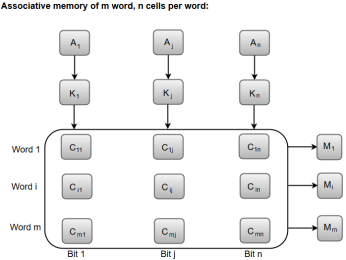
Fig 11: The relation between the memory array and the external registers in an associative memory
The cells present inside the memory array are marked by the letter C with two subscripts. The first subscript gives the word number and the second specifies the bit position in the word. For instance, the cell Cij is the cell for bit j in word i.
A bit Aj in the argument register is compared with all the bits in column j of the array provided that Kj = 1. This process is done for all columns j = 1, 2, 3......, n.
If a match occurs between all the unmasked bits of the argument and the bits in word i, the corresponding bit Mi in the match register is set to 1. If one or more unmasked bits of the argument and the word do not match, Mi is cleared to 0.
Q17) What do you mean by interleaving?
A17) Memory is divided into small parts via interleaving. It's a high-level method for resolving memory issues in motherboards and processors. The overall performance of the processor and system improves by raising bandwidth so data may reach portions of memory. Because the CPU can fetch and send more data to and from memory in the same amount of time, this is the case.
Interleaving is the only approach that all motherboards support. Implementing such strategies necessitates the use of high-level processing management systems on a regular basis. For servers in large enterprises, interleaving enhances efficient database and communication.
It's a method of compensating for DRAM's comparatively poor speed (Dynamic RAM). The primary memory is separated into memory banks in this technique, each of which can be accessed independently of the others.
Memory interleaving is a memory-speed-improving technology. It is a procedure that improves the system's efficiency, speed, and dependability.
Memory interleaving is the concept of partitioning main memory into multiple modules or banks, each of which interacts with the CPU independently of the others. Memory address and data registers are unique to each memory module. The Memory Address Register (MAR) is linked to a common unidirectional memory bus, whereas the data register is linked to a common data bus.
When the CPU requests data, the address is sent to memory through the common memory bus. The memory address register saves the address. Data is now retrieved from the module and stored in the data register before being transferred to the CPU through the common data bus.
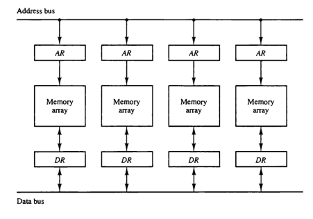
Types of interleaving
Interleaving comes in a variety of forms:
Two way interleaving - For reading and writing operations, two memory blocks are accessible at the same level. There is a possibility of overlap.
Four way interleaving - At the same moment, four memory blocks are accessed.
Error correction interleaving - Rather than being a single attack, communication system errors occur in large numbers. Interleaving uses specific techniques to control these issues.
Q18) What is virtual memory?
A18) A computer can address more memory than the amount physically installed on the system. This extra memory is actually called virtual memory and it is a section of a hard disk that's set up to emulate the computer's RAM.
The main visible advantage of this scheme is that programs can be larger than physical memory. Virtual memory serves two purposes. First, it allows us to extend the use of physical memory by using disk. Second, it allows us to have memory protection, because each virtual address is translated to a physical address.
Following are the situations, when entire program is not required to be loaded fully in main memory.
● User written error handling routines are used only when an error occurred in the data or computation.
● Certain options and features of a program may be used rarely.
● Many tables are assigned a fixed amount of address space even though only a small amount of the table is actually used.
● The ability to execute a program that is only partially in memory would counter many benefits.
● Less number of I/O would be needed to load or swap each user program into memory.
● A program would no longer be constrained by the amount of physical memory that is available.
● Each user program could take less physical memory, more programs could be run the same time, with a corresponding increase in CPU utilization and throughput.
Modern microprocessors intended for general-purpose use, a memory management unit, or MMU, is built into the hardware. The MMU's job is to translate virtual addresses into physical addresses. A basic example is given below −
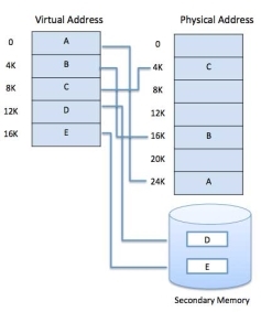
Fig 12: Memory Address
Virtual memory is commonly implemented by demand paging. It can also be implemented in a segmentation system. Demand segmentation can also be used to provide virtual memory.
Demand Paging
A demand paging system is quite similar to a paging system with swapping where processes reside in secondary memory and pages are loaded only on demand, not in advance. When a context switch occurs, the operating system does not copy any of the old program’s pages out to the disk or any of the new program’s pages into the main memory Instead, it just begins executing the new program after loading the first page and fetches that program’s pages as they are referenced.
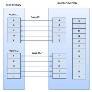
Fig 13: Swap in swap out
While executing a program, if the program references a page which is not available in the main memory because it was swapped out a little ago, the processor treats this invalid memory reference as a page fault and transfers control from the program to the operating system to demand the page back into the memory.
Advantages
Following are the advantages of Demand Paging −
● Large virtual memory.
● More efficient use of memory.
● There is no limit on degree of multiprogramming.
Disadvantages
● Number of tables and the amount of processor overhead for handling page interrupts are greater than in the case of the simple paged management techniques.
Q19) Define page replacement algorithm?
A19) Page Replacement Algorithm
Page replacement algorithms are the techniques using which an Operating System decides which memory pages to swap out, write to disk when a page of memory needs to be allocated. Paging happens whenever a page fault occurs and a free page cannot be used for allocation purpose accounting to reason that pages are not available or the number of free pages is lower than required pages.
When the page that was selected for replacement and was paged out, is referenced again, it has to read in from disk, and this requires for I/O completion. This process determines the quality of the page replacement algorithm: the lesser the time waiting for page-ins, the better is the algorithm.
A page replacement algorithm looks at the limited information about accessing the pages provided by hardware, and tries to select which pages should be replaced to minimize the total number of page misses, while balancing it with the costs of primary storage and processor time of the algorithm itself. There are many different page replacement algorithms. We evaluate an algorithm by running it on a particular string of memory reference and computing the number of page faults,
Reference String
The string of memory references is called reference string. Reference strings are generated artificially or by tracing a given system and recording the address of each memory reference. The latter choice produces a large number of data, where we note two things.
● For a given page size, we need to consider only the page number, not the entire address.
● If we have a reference to a page p, then any immediately following references to page p will never cause a page fault. Page p will be in memory after the first reference; the immediately following references will not fault.
● For example, consider the following sequence of addresses − 123,215,600,1234,76,96
● If page size is 100, then the reference string is 1,2,6,12,0,0
First In First Out (FIFO) algorithm
● Oldest page in main memory is the one which will be selected for replacement.
● Easy to implement, keep a list, replace pages from the tail and add new pages at the head.
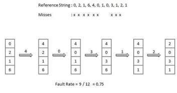
Optimal Page algorithm
● An optimal page-replacement algorithm has the lowest page-fault rate of all algorithms. An optimal page-replacement algorithm exists, and has been called OPT or MIN.
● Replace the page that will not be used for the longest period of time. Use the time when a page is to be used.
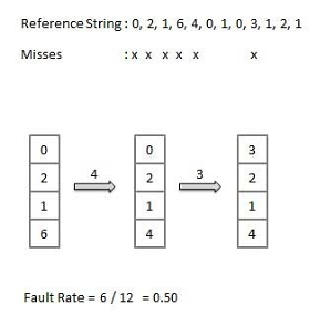
Least Recently Used (LRU) algorithm
● Page which has not been used for the longest time in main memory is the one which will be selected for replacement.
● Easy to implement, keep a list, replace pages by looking back into time.
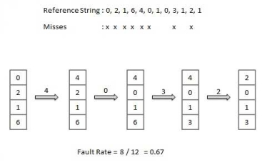
Page Buffering algorithm
● To get a process start quickly, keep a pool of free frames.
● On page fault, select a page to be replaced.
● Write the new page in the frame of free pool, mark the page table and restart the process.
● Now write the dirty page out of disk and place the frame holding replaced page in free pool.
Least frequently Used (LFU) algorithm
● The page with the smallest count is the one which will be selected for replacement.
● This algorithm suffers from the situation in which a page is used heavily during the initial phase of a process, but then is never used again.
Most frequently Used (MFU) algorithm
● This algorithm is based on the argument that the page with the smallest count was probably just brought in and has yet to be used.
Q20) Describe memory management?
A20) Memory is separated into two sections in any programming system, one for the operating system and the other for the program now being executed.
The user section of memory in a multiprogramming system is partitioned to support several processes.
The task of subdivision is known as memory management, and it is performed dynamically by the operating system.
Only one program is running in a uniprogramming system. Following the completion of one program, another program may begin.
The majority of programs, in general, involve I/O operations. It must receive data from various input devices and output the results to various output devices.
Figure shows the main memory partitioning for the Union program and multiprogramming.
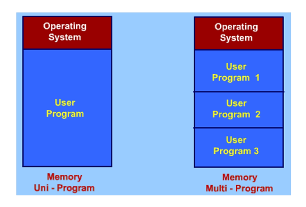
Fig 14: Partition of main memory
They are changing the paradigm from a Uniprogramming environment to a multiprogramming one in order to take advantage of the CPU's idle time.
Because the size of main memory is fixed, only a few processes can be accommodated in the main memory. If everyone is waiting for an I/O activity, the CPU will remain idle.
To make use of the CPU's idle time, some processes must be offloaded from memory and other processes must be introduced to this memory location. Swapping is the term for this.
Swapping
Swapping is a mechanism for temporarily moving a process from main memory to secondary storage (disk) and making that memory available to other processes. The system switches the process from secondary storage to main memory at a later time.
Though the swapping process degrades performance, it aids in the concurrent execution of various and large processes, which is why it's also known as a memory compression approach.
Partitioning
Two types Memory is divided into parts to be allocated to processes (including Operating System).
● Fixed-sized partitions
● Variable-sized partitions
Fixed size Partitions
Partitions of equal or unequal size. The process is crammed into the tiniest hole available (best fit).
Because each block has a hole of idle memory at the end of its partition, some memory is wasted. This results in partitions of varying sizes.
Below are examples of fixed size main memory partitions of equal and unequal size.
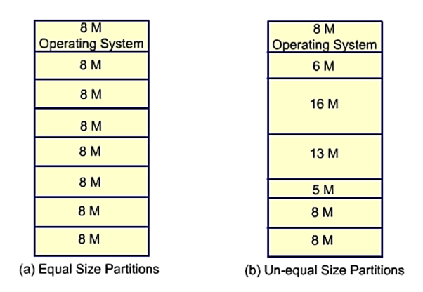
Fig 15: Equal and unequal size partition
There will be memory waste even if the partitions are of uneven size. In most circumstances, a process will not require exactly the same amount of memory as the partition provides.
A task that uses 5 MB of RAM, for example, would be placed in the 6mb partition, which is the smallest one accessible. Only 5 MB is used in this partition; the remaining 1 MB cannot be used by any other process, hence it is a waste. As a result, we may have some unused memory in each partition. Each partition's unused memory partition is referred to as a hole.
Variable size partition
When a process is brought into memory, it is given exactly the amount of memory it needs and nothing more. This results in a hole at the end of the memory that is too small to be useful. There appears to be only one hole at the end, resulting in less waste.
However, this isn't the only flaw that variable-size partitions will have. When all processes have been blocked, switch out one and bring in another. It's possible that the new switched in process will be smaller than the swapped out process. We will most likely not be able to process the same size. As a result, it will form a new whole. If the swap out and swap in happens more frequently, a larger hole will be created, resulting in more memory waste.
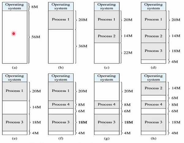
Fig 16: Variable size partition