Unit - 3
Combinational Circuits Design
Q1) What is a Multiplexer? Explain 2:1 Mux in detail.
A1)
- It is a special type of combinational circuit.
- It has n-data inputs, one output and m inputs select lines with 2m = n.
- It selects one of the n data inputs and routes it to the output.
- The selection of one of the inputs is done by the select lines.
- Depending on the code applied at the inputs, one of the n data sources is selected and transmitted to the single output Y.
- E is the enable input which is useful for cascading purpose.
- It is an active low terminal hence performs the required operation when it is low.
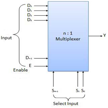
Block diagram of multiplexer
Multiplexers come in multiple variations
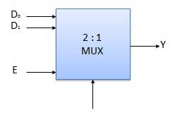
- 2 : 1 multiplexer
- 4 : 1 multiplexer
- 16 : 1 multiplexer
- 32 : 1 multiplexer
Block Diagram of 2:1 MUX
Truth Table of 2:1 MUX
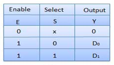
Where x is don’t care.
Q2) Draw and explain Full adder.
A2)
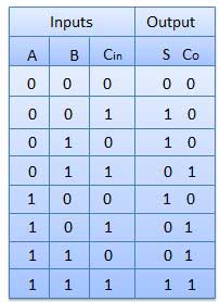
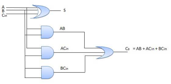
- It is developed to overcome the drawback of Half Adder circuit.
- It can add two one-bit numbers A and B and a carry C.
- It is a three input and two output combinational circuit.
Block diagram
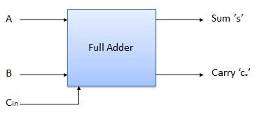
Full adder
Truth Table
Circuit Diagram
Full adder
Q3) Draw and explain Full Subtractor.
A3)
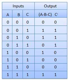
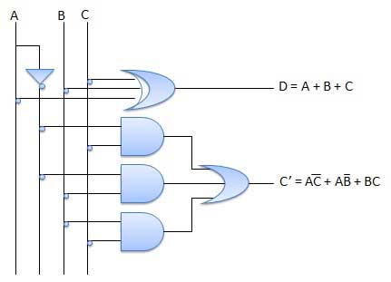
It is a combinational circuit which has three inputs A,B,C and two output D and C'.
A is the 'minuend', B is 'subtrahend', C is the 'borrow' which is produced by the previous stage, difference output D and C' is the borrow output.
Truth Table
Circuit Diagram
Full subtractor
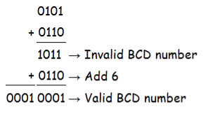
Q4) Do BCD addition of 0101 with 0110.
A4)

Q5) Explain look ahead carry adder with circuit diagram.
A5)
- In this, for each adder block, the two bits that are to be added are available instantly.
- However, each of them waits for the carry to arrive from the previous one.
- So, it is impossible to generate the sum and carry of any block until the input carry is known.
- The block waits for the previous block to produce its carry. So there will be a considerable time delay which is known as carry propagation delay.

- Here, the sum is produced by the corresponding full adder as soon as the input signals are applied to it. The carry must propagate to all the stages so that output and carry settle their final steady-state value.
- The propagation time is equal to the propagation delay of each adder block, multiplied by the number of adder blocks in the circuit.
- It reduces the propagation delay by introducing more complex hardware.
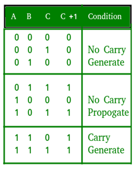
- The ripple carry design is suitably transformed in such a way that the carry logic over fixed groups of bits is reduced to two-level logic.
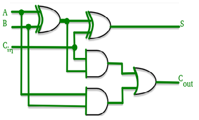
Look ahead Carry adder
Q6) Explain digital comparator with its applications.
A6)
- It performs comparison operation with more than four bits by cascading two or more 4-bit comparators.
- When two comparators are to be cascaded, the outputs of the lower-order comparator is connected to corresponding input of the higher-order comparator.
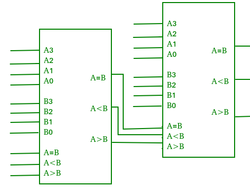
Digital comparator
Applications of Comparators –
- They are used in central processing units (CPUs) and microcontrollers (MCUs).
- They are used in control applications where the binary numbers represents physical variables such as temperature, position, etc. and are compared with a reference value.
- They are also used as process controllers and Servo motor controllers.
- They are used in password verification and biometric applications too.
Q7) Explain even parity generator with example.
A7)
A 3-bit message is transmitted with an even parity bit. Hence assuming, the three inputs W,X and Y that are applied to the circuits and output bit is the parity bit P. The total number of 1s must be even, to generate the even parity bit P.
3- bit message | Even Parity | ||
W | X | Y | P |
0 | 0 | 0 | 0 |
0 | 0 | 1 | 1 |
0 | 1 | 0 | 1 |
0 | 1 | 1 | 0 |
1 | 0 | 0 | 1 |
1 | 0 | 1 | 0 |
1 | 1 | 0 | 0 |
1 | 1 | 1 | 1 |
The K-map simplification for 3-bit message even parity generator is
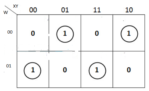
From the above K-Map, the expression is:
P=W′X′Y+W′XY′+WX′Y′+WXY
P=W′(X′Y+XY′)+W(X′Y′+XY)
P=W′(X⊕Y)+W(X⊕Y)′=W⊕X⊕Y

Q8) Explain even parity checker with example.
A8)
Assume a 3-bit binary input, W, X and Y is transmitted along with an even parity bit, P. So, the resultant data contains 4 bits, that is received as the input of even parity checker.
It generates an even parity bit, E. This bit is zero, if the received data contains an even number of ones, which indicates that there is no error in the received data and vice versa.
The Truth table of an even parity checker is:
4-bit Received Data WXYP | Even Parity Check bit E |
0000 | 0 |
0001 | 1 |
0010 | 1 |
0011 | 0 |
0100 | 1 |
0101 | 0 |
0110 | 0 |
0111 | 1 |
1000 | 1 |
1001 | 0 |
1010 | 0 |
1011 | 1 |
1100 | 0 |
1101 | 1 |
1110 | 1 |
1111 | 0 |
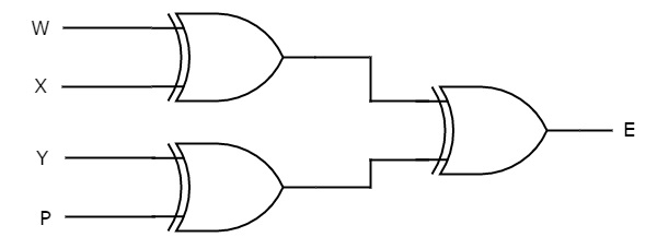
The Boolean function of even parity check bit as
E = W xor X xor Y xor P
The following figure shows the circuit diagram of even parity checker.
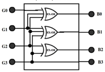
Q9) Convert Gray code To Binary Code.
A9)
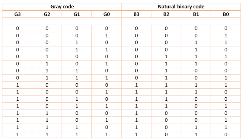
Then the K-maps:
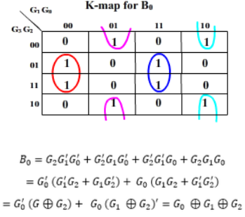


And B3 = G3
The realization of Gray-to-Binary converter is
Q10) Implement 3:8 Decoder.
A10)
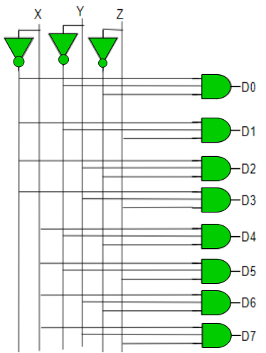
D0 is high when X = 0, Y = 0 and Z = 0. Hence,
D0 = X’ Y’ Z’
Similarly,
D1 = X’ Y’ Z
D2 = X’ Y Z’
D3 = X’ Y Z
D4 = X Y’ Z’
D5 = X Y’ Z
D6 = X Y Z’
D7 = X Y Z
Hence,
Decoder