Unit - 5
Logic Families and VLSI Design flow
Q1) Explain RTL in detail.
A1)
Register-transfer-level is used in hardware description languages (HDLs) such as Verilog and VHDL to create high-level representations of a circuit.
It consists of registers (Sequential logic) and combinational logic.
Registers (usually implemented with the help of D flip-flops) synchronize the circuit's operation to the edges of the clock signal, and consists of memory properties. Combinational logic performs all the logical functions in the circuit and it is made up of logic gates.
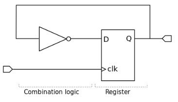
Fig. 1:RTL
It is used in the logic design phase of the integrated circuit.
The most accurate power analysis tools are present for the circuit level have disadvantages like they are slow and require too much memory for large chip handling.
Q2) Write advantages and disadvantages of RTL.
A2)
Advantages
- The design is used to make optimizations and trade-offs.
- The presence of functional blocks makes the complexity of architectural design more manageable because it has larger gate- or circuit-level descriptions.
Disadvantages
- The modeling of circuit activities is not accurate.
- The activity factor that is chosen gives the correct total power, clock, memory, etc. that is less accurate.
Q3) Explain DTL in detail.
A3)
Diode–transistor logic (DTL) is a class of digital circuits in which the logic gating function is done by a diode network and the amplification is performed by a transistor.
The DTL circuit shown in the figure below and it consists of three stages: an input diode logic stage (D1, D2 and R1), an intermediate level shifting stage (R3 and R4), and an output common-emitter amplifier stage (Q1 and R2).
If both inputs A and B are high, then the diodes D1 and D2 are reverse biased. Resistors R1 and R3 will then supply sufficient current to turn on Q1 and also supply the current needed by R4. There is a small amount of positive voltage on the base of Q1. The turned on transistor's collector current will pull the output Q low.
If any of the inputs are low, then at least one of the diodes conduct. R3 and R4 act as a voltage divider making Q1's base voltage negative and consequently turning off . Collector current from Q1 will be zero, so R2 will pull the output voltage Q high.

Fig.2: DTL
Q4) Write advantages and disadvantages of DTL.
A4)
Advantages
- The propagation delay is relatively large.
- It has increased fan-in, fan-out, an additional transistor and diode can be used.
Disadvantages
- It has low speed in comparison to TTL.
Q5) Explain TTL.
A5)
Transistor-transistor logic (TTL) is a class of integrated circuits that maintains logic states and switches with the help of bipolar transistors.
It inputs rise to the logic "1" if left unconnected. It is one of the reasons that integrated circuits are widely used, as they are cheap, reliable and faster than RTL and DTL.
TTL makes use of transistors with multiple emitters in gates having multiple inputs.
The family of TTL is as follows:
- Standard TTL
It is used for 3.3-volt power supplies and memory interfacing.
- Fast TTL
It has faster switching than (6ns) but significantly higher power dissipation (22 mW).
- Schottky TTL
It uses Schottky diode clamps at gate inputs to prevent charge storage and improve switching time.
- Low power Schottky TTL
It is used for high resistance values of low-power TTL and the Schottky diodes provide a good combination of speed (9.5ns) and reduce power consumption (2 mW) too.
- Low power TTL
It is traded switching speed (33ns) for a reduction in power consumption (1 mW).
- Advanced Schottky TTL
It speeds up the low-to-high transition of TTL.
Advantages
- It is relatively easy in interfacing different circuits and produce complex logic functions.
- It has good noise margins as well as guaranteed voltage levels.
- It has good fan-in and is largely immune to damage from static electricity discharges
Disadvantages
- It has limited speed, low frequency, very noisy, high power consumption at higher frequencies.

Fig.3: TTL
Q6) What is a MOSFET? Explain PMOS and NMOS.
A6)
The MOSFET (metal-oxide-semiconductor field-effect transistor) are of two types: PMOS (p-type MOS) and NMOS (n-type MOS).
A new type of MOSFET logic is made combining both the PMOS and NMOS processes and is called as complementary MOS (CMOS).
CMOS stands for “Complementary Metal Oxide Semiconductor”.
It is one of the most popular technology in the chip design industry and is used today to form integrated circuits for various applications.
Computer memories, CPUs and cell phones make use of this technology due to various advantages. This technology uses both P and N channel semiconductor devices.
NMOS
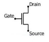
NMOS is built on a p-type substrate with n-type source and drain diffused on it. Here, the majority carriers are electrons. When a high voltage is applied to the gate, the NMOS conducts and when low voltage is applied to the gate, it does not conduct. NMOS is faster than PMOS, as the carriers are electrons that travel twice as fast as the holes.
PMOS
P-MOS consists of P-type Source and Drain diffused on an N-type substrate. Here, majority carriers are holes. When a high voltage is applied to the gate, the PMOS does not conduct and when a low voltage is applied, it conducts. These devices are more immune to noise than NMOS devices.

CMOS Applications
- Computer memories, CPUs
- Microprocessor designs
- Flash memory chip designing
- Used to design application specific integrated circuits (ASICs)
Advantages
- The power dissipation is very small.
- Greater number of IC’s can be integrated on a single chip.

Fig.4: CMOS
Q7) Explain IIL.
A7)
Integrated injection logic (IIL, I2L, or I2L) are built with multiple collector bipolar junction transistors (BJT).
It had speed near to TTL and as low power as CMOS, hence ideal for use in VLSI (and larger) integrated circuits.
It is simple to construct on an integrated circuit and used before the introduction of CMOS logic by companies such as Motorola and Texas Instruments.
2L gates were constructed with transistors with 1, 2 or 3 separate collectors. This fan-out allowed 3-input NAND or NOR gates to be constructed with just a single layer of interconnect metal.
The heart of an I2L circuit is made of common emitter open collector inverter.
Advantages
- Low power dissipation
- Number of processing steps required is small; hence cost per gate is low.
Disadvantages
- Lower packing density than NMOS.
- Lower noise margin.
Q8) Compare IIL, RTL, DTL, ECL, MOS.
A8)

Q9) Write a code for 4:1 MUX.
A9)
Library IEEE;
Use IEEE.STD_LOGIC_1164.ALL;
Use IEEE.STD_LOGIC_ARITH.ALL;
Use IEEE.STD_LOGIC_UNSIGNED.ALL;
Entity MUX_SOURCE is
Port ( S : in STD_LOGIC_VECTOR (1 downto 0);
I : in STD_LOGIC_VECTOR (3 downto 0);
Y : out STD_LOGIC);
End MUX_SOURCE;
Architecture Behavioral of MUX_SOURCE is
Begin
Process (S,I)
Begin
If (S <= "00") then
Y <= I(0);
Elsif (S <= "01") then
Y <= I(1);
Elsif (S <= "10") then
Y <= I(2);
Else
Y <= I(3);
End if;
End process;
End Behavioral;
Q10) Write a code for full adder.
A10)
Library IEEE;
Use IEEE.STD_LOGIC_1164.ALL;
Use IEEE.STD_LOGIC_ARITH.ALL;
Use IEEE.STD_LOGIC_UNSIGNED.ALL;
Entity FULLADDER_BEHAVIORAL_SOURCE is
Port ( A : in STD_LOGIC_VECTOR (2 downto 0);
O : out STD_LOGIC_VECTOR (1 downto 0));
End FULLADDER_BEHAVIORAL_SOURCE;
Architecture Behavioral of FULLADDER_BEHAVIORAL_SOURCE is
Begin
Process (A)
Begin
—for SUM
If (A = “001” or A = “010” or A = “100” or A = “111”) then
O(1) <= ‘1’;
—single inverted commas used for assigning to one bit
Else
O(1) < = ‘0’;
End if;
—for CARRY
If (A = “011” or A = “101” or A = “110” or A = “111”) then
O(0) <= ‘1’;
Else
O(0) <<= ‘0’;
End if;
End process;
End Behavioral;
Q11) Write a code for
A11)
Library IEEE;
Use IEEE.STD_LOGIC_1164.ALL;
Use IEEE.STD_LOGIC_ARITH.ALL;
Use IEEE.STD_LOGIC_UNSIGNED.ALL;
Entity and_or is
Port(
a : in std_logic;
b : in std_logic;
d : in std_logic;
e : in std_logic;
g : out std_logic);
End and_or;
Architecture and_or_a of and_or is
-- declarative part: empty
Begin
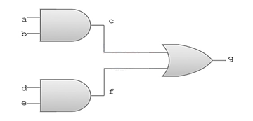
g <= (a and b) or (d and e);
End and_or_a;
Q12) Write a code for JK flip-flop.
A12)
Library IEEE;
use IEEE.STD_LOGIC_1164.all;
entity jk is
port(
j : in STD_LOGIC;
k : in STD_LOGIC;
clk : in STD_LOGIC;
reset : in STD_LOGIC;
q : out STD_LOGIC;
qb : out STD_LOGIC
);
end jk;
architecture jk_flip_flop of jk is
begin
jkff : process (j,k,clk,reset) is
variable m : std_logic := '0';
begin
if (reset='1') then
m := '0';
elsif (rising_edge (clk)) then
if (j/=k) then
m := j;
elsif (j='1' and k='1') then
m := not m;
end if;
end if;
q <= m;
qb <= not m;
end process jkff;
end jk_flip_flop;
Q13) Write a code for RS latch.
A13)
Library IEEE;
use IEEE.STD_LOGIC_1164.all;
entity SR_Latch is
port(
enable : in STD_LOGIC;
s : in STD_LOGIC;
r : in STD_LOGIC;
reset : in STD_LOGIC;
q : out STD_LOGIC;
qb : out STD_LOGIC );
end SR_Latch;
architecture SR_Latch_arc of SR_Latch is
begin
latch : process (s,r,enable,reset) is
begin
if (reset='1') then
q <= '0';
qb <= '1';
elsif (enable='1') then
if (s/=r) then
q <= s;
qb <= r;
elsif (s='1' and r='1') then
q <= 'Z';
qb <= 'Z';
end if;
end if;
end process latch;
end SR_Latch_arc;
Q14) Write a VHDL code for Mealy machine.
A14)

Type state_type is (S0, S1);
Signal state, next_state : state_type;
Begin
SYNC_PROC : process (clk)
Begin
If rising_edge(clk) then
If (reset = '1') then
State <= S0;
Else state <= next_state;
End if;
End if;
End process;
NEXT_STATE_DECODE : process (state, x)
Begin
Parity <= '0';
Case (state) is
When S0 =>
If (x = '1') then
Parity <= '1';
Next_state <= S1;
Else
Next_state <= S0;
End if;
When S1 =>
If (x = '1') then
Next_state <= S0;
Else
Parity <= '1';
Next_state <= S1;
End if;
When others =>
Next_state <= S0;
End case;
End process;
Q15) Write a VHDL code for Moore machine.
A15)

Type state_type is (S0, S1);
Signal state, next_state : state_type;
Begin
SYNC_PROC : process (clk)
Begin
If rising_edge(clk) then
If (reset = '1') then
State <= S0;
Else
State <= next_state;
End if;
End process;
OUTPUT_DECODE : process (state)
Begin
Case (state) is
When S0 =>
Parity <= '0';
When S1 =>
Parity <= '1';
When others =>
Parity <= '0';
End case;
End process;
NEXT_STATE_DECODE : process (state, x)
Begin
Next_state <= S0;
Case (state) is
When S0 =>
If (x = '1') then
Next_state <= S1;
End if;
When S1 =>
If (x = '0') then
Next_state <= S1;
End if;
When others => next_state <= S0;
End case;
End process;
Unit - 5
Logic Families and VLSI Design flow
Q1) Explain RTL in detail.
A1)
Register-transfer-level is used in hardware description languages (HDLs) such as Verilog and VHDL to create high-level representations of a circuit.
It consists of registers (Sequential logic) and combinational logic.
Registers (usually implemented with the help of D flip-flops) synchronize the circuit's operation to the edges of the clock signal, and consists of memory properties. Combinational logic performs all the logical functions in the circuit and it is made up of logic gates.

Fig. 1:RTL
It is used in the logic design phase of the integrated circuit.
The most accurate power analysis tools are present for the circuit level have disadvantages like they are slow and require too much memory for large chip handling.
Q2) Write advantages and disadvantages of RTL.
A2)
Advantages
- The design is used to make optimizations and trade-offs.
- The presence of functional blocks makes the complexity of architectural design more manageable because it has larger gate- or circuit-level descriptions.
Disadvantages
- The modeling of circuit activities is not accurate.
- The activity factor that is chosen gives the correct total power, clock, memory, etc. that is less accurate.
Q3) Explain DTL in detail.
A3)
Diode–transistor logic (DTL) is a class of digital circuits in which the logic gating function is done by a diode network and the amplification is performed by a transistor.
The DTL circuit shown in the figure below and it consists of three stages: an input diode logic stage (D1, D2 and R1), an intermediate level shifting stage (R3 and R4), and an output common-emitter amplifier stage (Q1 and R2).
If both inputs A and B are high, then the diodes D1 and D2 are reverse biased. Resistors R1 and R3 will then supply sufficient current to turn on Q1 and also supply the current needed by R4. There is a small amount of positive voltage on the base of Q1. The turned on transistor's collector current will pull the output Q low.
If any of the inputs are low, then at least one of the diodes conduct. R3 and R4 act as a voltage divider making Q1's base voltage negative and consequently turning off . Collector current from Q1 will be zero, so R2 will pull the output voltage Q high.
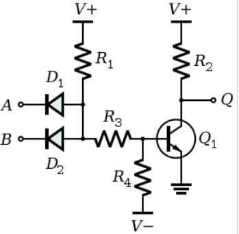
Fig.2: DTL
Q4) Write advantages and disadvantages of DTL.
A4)
Advantages
- The propagation delay is relatively large.
- It has increased fan-in, fan-out, an additional transistor and diode can be used.
Disadvantages
- It has low speed in comparison to TTL.
Q5) Explain TTL.
A5)
Transistor-transistor logic (TTL) is a class of integrated circuits that maintains logic states and switches with the help of bipolar transistors.
It inputs rise to the logic "1" if left unconnected. It is one of the reasons that integrated circuits are widely used, as they are cheap, reliable and faster than RTL and DTL.
TTL makes use of transistors with multiple emitters in gates having multiple inputs.
The family of TTL is as follows:
- Standard TTL
It is used for 3.3-volt power supplies and memory interfacing.
- Fast TTL
It has faster switching than (6ns) but significantly higher power dissipation (22 mW).
- Schottky TTL
It uses Schottky diode clamps at gate inputs to prevent charge storage and improve switching time.
- Low power Schottky TTL
It is used for high resistance values of low-power TTL and the Schottky diodes provide a good combination of speed (9.5ns) and reduce power consumption (2 mW) too.
- Low power TTL
It is traded switching speed (33ns) for a reduction in power consumption (1 mW).
- Advanced Schottky TTL
It speeds up the low-to-high transition of TTL.
Advantages
- It is relatively easy in interfacing different circuits and produce complex logic functions.
- It has good noise margins as well as guaranteed voltage levels.
- It has good fan-in and is largely immune to damage from static electricity discharges
Disadvantages
- It has limited speed, low frequency, very noisy, high power consumption at higher frequencies.
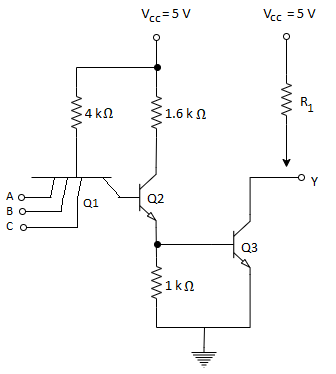
Fig.3: TTL
Q6) What is a MOSFET? Explain PMOS and NMOS.
A6)
The MOSFET (metal-oxide-semiconductor field-effect transistor) are of two types: PMOS (p-type MOS) and NMOS (n-type MOS).
A new type of MOSFET logic is made combining both the PMOS and NMOS processes and is called as complementary MOS (CMOS).
CMOS stands for “Complementary Metal Oxide Semiconductor”.
It is one of the most popular technology in the chip design industry and is used today to form integrated circuits for various applications.
Computer memories, CPUs and cell phones make use of this technology due to various advantages. This technology uses both P and N channel semiconductor devices.
NMOS
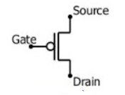
NMOS is built on a p-type substrate with n-type source and drain diffused on it. Here, the majority carriers are electrons. When a high voltage is applied to the gate, the NMOS conducts and when low voltage is applied to the gate, it does not conduct. NMOS is faster than PMOS, as the carriers are electrons that travel twice as fast as the holes.

PMOS
P-MOS consists of P-type Source and Drain diffused on an N-type substrate. Here, majority carriers are holes. When a high voltage is applied to the gate, the PMOS does not conduct and when a low voltage is applied, it conducts. These devices are more immune to noise than NMOS devices.
CMOS Applications
- Computer memories, CPUs
- Microprocessor designs
- Flash memory chip designing
- Used to design application specific integrated circuits (ASICs)
Advantages
- The power dissipation is very small.
- Greater number of IC’s can be integrated on a single chip.
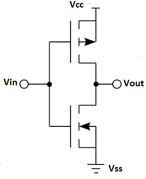
Fig.4: CMOS
Q7) Explain IIL.
A7)
Integrated injection logic (IIL, I2L, or I2L) are built with multiple collector bipolar junction transistors (BJT).
It had speed near to TTL and as low power as CMOS, hence ideal for use in VLSI (and larger) integrated circuits.
It is simple to construct on an integrated circuit and used before the introduction of CMOS logic by companies such as Motorola and Texas Instruments.
2L gates were constructed with transistors with 1, 2 or 3 separate collectors. This fan-out allowed 3-input NAND or NOR gates to be constructed with just a single layer of interconnect metal.
The heart of an I2L circuit is made of common emitter open collector inverter.
Advantages
- Low power dissipation
- Number of processing steps required is small; hence cost per gate is low.
Disadvantages
- Lower packing density than NMOS.
- Lower noise margin.
Q8) Compare IIL, RTL, DTL, ECL, MOS.
A8)
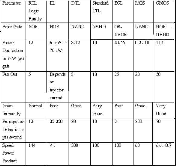
Q9) Write a code for 4:1 MUX.
A9)
Library IEEE;
Use IEEE.STD_LOGIC_1164.ALL;
Use IEEE.STD_LOGIC_ARITH.ALL;
Use IEEE.STD_LOGIC_UNSIGNED.ALL;
Entity MUX_SOURCE is
Port ( S : in STD_LOGIC_VECTOR (1 downto 0);
I : in STD_LOGIC_VECTOR (3 downto 0);
Y : out STD_LOGIC);
End MUX_SOURCE;
Architecture Behavioral of MUX_SOURCE is
Begin
Process (S,I)
Begin
If (S <= "00") then
Y <= I(0);
Elsif (S <= "01") then
Y <= I(1);
Elsif (S <= "10") then
Y <= I(2);
Else
Y <= I(3);
End if;
End process;
End Behavioral;
Q10) Write a code for full adder.
A10)
Library IEEE;
Use IEEE.STD_LOGIC_1164.ALL;
Use IEEE.STD_LOGIC_ARITH.ALL;
Use IEEE.STD_LOGIC_UNSIGNED.ALL;
Entity FULLADDER_BEHAVIORAL_SOURCE is
Port ( A : in STD_LOGIC_VECTOR (2 downto 0);
O : out STD_LOGIC_VECTOR (1 downto 0));
End FULLADDER_BEHAVIORAL_SOURCE;
Architecture Behavioral of FULLADDER_BEHAVIORAL_SOURCE is
Begin
Process (A)
Begin
—for SUM
If (A = “001” or A = “010” or A = “100” or A = “111”) then
O(1) <= ‘1’;
—single inverted commas used for assigning to one bit
Else
O(1) < = ‘0’;
End if;
—for CARRY
If (A = “011” or A = “101” or A = “110” or A = “111”) then
O(0) <= ‘1’;
Else
O(0) <<= ‘0’;
End if;
End process;
End Behavioral;
Q11) Write a code for

A11)
Library IEEE;
Use IEEE.STD_LOGIC_1164.ALL;
Use IEEE.STD_LOGIC_ARITH.ALL;
Use IEEE.STD_LOGIC_UNSIGNED.ALL;
Entity and_or is
Port(
a : in std_logic;
b : in std_logic;
d : in std_logic;
e : in std_logic;
g : out std_logic);
End and_or;
Architecture and_or_a of and_or is
-- declarative part: empty
Begin
g <= (a and b) or (d and e);
End and_or_a;
Q12) Write a code for JK flip-flop.
A12)
Library IEEE;
use IEEE.STD_LOGIC_1164.all;
entity jk is
port(
j : in STD_LOGIC;
k : in STD_LOGIC;
clk : in STD_LOGIC;
reset : in STD_LOGIC;
q : out STD_LOGIC;
qb : out STD_LOGIC
);
end jk;
architecture jk_flip_flop of jk is
begin
jkff : process (j,k,clk,reset) is
variable m : std_logic := '0';
begin
if (reset='1') then
m := '0';
elsif (rising_edge (clk)) then
if (j/=k) then
m := j;
elsif (j='1' and k='1') then
m := not m;
end if;
end if;
q <= m;
qb <= not m;
end process jkff;
end jk_flip_flop;
Q13) Write a code for RS latch.
A13)
Library IEEE;
use IEEE.STD_LOGIC_1164.all;
entity SR_Latch is
port(
enable : in STD_LOGIC;
s : in STD_LOGIC;
r : in STD_LOGIC;
reset : in STD_LOGIC;
q : out STD_LOGIC;
qb : out STD_LOGIC );
end SR_Latch;
architecture SR_Latch_arc of SR_Latch is
begin
latch : process (s,r,enable,reset) is
begin
if (reset='1') then
q <= '0';
qb <= '1';
elsif (enable='1') then
if (s/=r) then
q <= s;
qb <= r;
elsif (s='1' and r='1') then
q <= 'Z';
qb <= 'Z';
end if;
end if;
end process latch;
end SR_Latch_arc;
Q14) Write a VHDL code for Mealy machine.
A14)
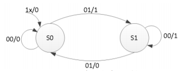
Type state_type is (S0, S1);
Signal state, next_state : state_type;
Begin
SYNC_PROC : process (clk)
Begin
If rising_edge(clk) then
If (reset = '1') then
State <= S0;
Else state <= next_state;
End if;
End if;
End process;
NEXT_STATE_DECODE : process (state, x)
Begin
Parity <= '0';
Case (state) is
When S0 =>
If (x = '1') then
Parity <= '1';
Next_state <= S1;
Else
Next_state <= S0;
End if;
When S1 =>
If (x = '1') then
Next_state <= S0;
Else
Parity <= '1';
Next_state <= S1;
End if;
When others =>
Next_state <= S0;
End case;
End process;
Q15) Write a VHDL code for Moore machine.
A15)
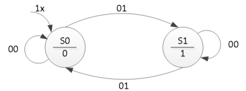
Type state_type is (S0, S1);
Signal state, next_state : state_type;
Begin
SYNC_PROC : process (clk)
Begin
If rising_edge(clk) then
If (reset = '1') then
State <= S0;
Else
State <= next_state;
End if;
End process;
OUTPUT_DECODE : process (state)
Begin
Case (state) is
When S0 =>
Parity <= '0';
When S1 =>
Parity <= '1';
When others =>
Parity <= '0';
End case;
End process;
NEXT_STATE_DECODE : process (state, x)
Begin
Next_state <= S0;
Case (state) is
When S0 =>
If (x = '1') then
Next_state <= S1;
End if;
When S1 =>
If (x = '0') then
Next_state <= S1;
End if;
When others => next_state <= S0;
End case;
End process;