Unit - 4
Power electronic devices & Communication engineering
Q1) A modulating signal m(t)=10cos(2π×103t) is amplitude modulated with a carrier signal c(t)=50cos(2π×105t). Find the modulation index, the carrier power, and the power required for transmitting AM wave.
A1) Given, the equation of modulating signal as
m(t)=10cos(2π×103t)
We know the standard equation of modulating signal as
m(t)=Am cos(2πfmt)
Comparing both equations, we get
Amplitude of modulating signal as Am=10volts
And Frequency of modulating signal as fm=103Hz=1KHz
c(t)=50cos(2π×105t)
Comparing these two equations, we will get
Amplitude of carrier signal as Ac=50volts
And Frequency of carrier signal as fc=105Hz=100KHz
μ = Am/Ac
μ = 10/50 =0.2
The value of modulation index is 0.2
Carrier power, Pc
Pc=Ac2/2R
Let R=1ohm
Carrier power, Pc is 1250 watts.


Q2) The equation of amplitude wave is given by s(t)=20[1+0.8cos(2π×103t)] cos(4π×105t). Find the carrier power, the total sideband power, and the band width of AM wave.
A2) s(t)=20[1+0.8cos(2π×103t)] cos(4π×105t).
We can write above equation as
s(t)=20[1+0.8cos(2π×103t)] cos (4πx 2 x105t).

Amplitude of carrier signal as Ac=20volts
Modulation index as μ=0.8
Frequency of modulating signal as fm=103Hz=1KHz
Frequency of carrier signal as fc=2×10⁵Hz=200KHz
The formula for Carrier power, Pc
Pc=Ac2/2R
Pc = (20)2/2(1) = 200W
Total side band power is
PSB=Pcμ2/2
PSB=200×(0.8)2/2=64W
Total side band power is 64 watts.
We know the formula for bandwidth of AM wave is
BW=2fm
Substitute fm value in the above formula.
BW=2(1K) =2KHz
The bandwidth of AM wave is 2 KHz.
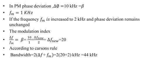
Q3) A carrier is phase modulated (PM) with frequency deviation of 10 kHz by a single tone frequency of 1 kHz. If the single tone frequency is increased to 2 kHz, assuming that phase deviation remains unchanged the bandwidth of the PM signal is
A3)
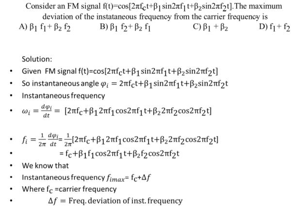
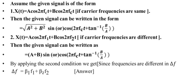
Q4) Consider an FM signal f(t)=cos[2πfct+1 sin2πf1t+2 sin2πf2t).The maximum deviation of the instataneous frequency from the carrier frequency is
A) 1 f1+ 2 f2 B) 1 f2+ 2 f1 C) 1 + 2 D) f1+ f2
A4)
Q5) A device with input 𝑥(𝑡) and output 𝑦(𝑡) is characterized by: 𝑦(𝑡)=𝑥2 (𝑡). An FM signal with frequency deviation of 90 KHz and modulating signal bandwidth of 5 KHz is applied to this device. The bandwidth of the output signal is (a) 370 KHz (b) 190 KHz (c) 380 KHz (d) 95 KHz
A5) Frequency deviation Δ𝒇=𝟗𝟎𝑲𝑯𝒛
Modulating signal bandwidth = 5 KMz
When FM signal is applied to doubler frequency deviation doubles.
𝑩.𝑾 = 𝟐(Δ𝒇+𝒇𝒎) = 𝟐(𝟏𝟖𝟎+𝟓) =𝟑𝟕𝟎 𝑲𝑯z
Q6) An FM signal with a modulation index 9 is applied to a frequency tripler. The modulation index in the output signal will be (a) 0 (b) 3 (c) 9 (d) 27
A6) The frequency modulation index β is multiplied by n in n-times frequency multiplier.
𝑺𝒐, 𝜷′=𝟑×𝟗 = 27
Q7) A sinusoidal modulating waveform of amplitude 5 V and a frequency of 2 KHz is applied to FM generator, which has a frequency sensitivity of 40 Hz/volt. Calculate the frequency deviation, modulation index, and bandwidth.
A7) Given, the amplitude of modulating signal, Am=5V
Frequency of modulating signal, fm=2KHz
Frequency sensitivity, kf=40Hz/volt
We know the formula for Frequency deviation as
Δf=kfAm
Δf=40×5=200Hz
β=Δf/fm
β=200/(2×1000) = 0.1
The formula for Bandwidth of Narrow Band FM is the same as that of AM wave.
BW=2fm
BW=2×2K=4KHz
Q8) An FM wave is given by s(t)=20cos(8π×106t+9sin(2π×103t)). Calculate the frequency deviation, bandwidth, and power of FM wave.
A8) s(t)=20cos(8π×106t+9sin(2π×103t))
We know the standard equation of an FM wave as
s(t)=Accos(2πfct+βsin(2πfmt))
Amplitude of the carrier signal, Ac=20V
Frequency of the carrier signal, fc=4×10⁶Hz=4MHz
Frequency of the message signal, fm=1×10³Hz=1KHz
Modulation index, β=9
β=Δf/fm
Δf=9×1K=9KHz
The formula for Bandwidth of Wide Band FM wave is
BW=2(β+1)fm
BW=2(9+1)1K=20KHz
The bandwidth of Wide Band FM wave is 20KHz
Pc=Ac2/2R
P= (20)2/2(1) =200W
Therefore, the power of FM wave is 200watts.
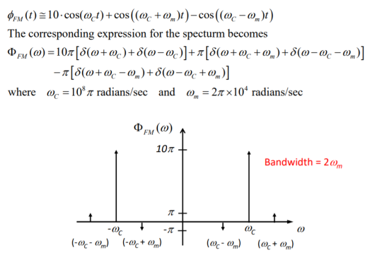
Q9) The message signal input to a modulator is m(t) = 4cos(2104 t) and the carrier is 10cos(108 t). If frequency modulation is performed with kf = 1000, verify that the modulated signal meets the criteria of being narrowband FM. Also, obtain an expression for its spectrum and sketch this spectrum.
A9)


Q10) For commercial FM radio, the audio message signal has a spectral range of 30 Hz to 15 kHz, and the FCC allows a frequency deviation of 75 kHz. Estimate the transmission bandwidth for commercial FM using Carson’s Rule.
A10) We know
β=Δf/fm = 75/15 =5
Using Carson's rule gives
BFM = 2(β+1)fm = 2(5+1)x15,000= 180kHz
The allowed bandwidth for commercial FM is 200 kHz.
Q11) Explain concept of modulation and demodulation?
A11)
- It is a process through which audio, video, image or text information is added to an electrical or optical carrier signal that is to be transmitted over a telecommunication or electronic medium.
- It enables the transfer of information on an electrical signal to a receiver that is capable of demodulating the signal to extract the blended information.
- It is primarily used in telecommunication technologies that require the transmission of data via electrical signals.
- It is considered the backbone of data communication as it enables the use of electrical and optical signals as information carriers.
- This is done by altering the periodic waveform or the carrier.
- This comprises of its amplitude, frequency and phase.
- Modulation has three different types:
- Amplitude Modulation (AM): Amplitude of the carrier is modulated.
- Frequency Modulation (FM): Frequency of the carrier is modulated.
- Phase Modulation (PM): Phase of the carrier is modulated.
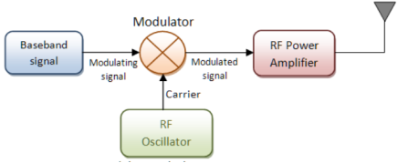
Fig: Modulation
Demodulation (downward frequency translation)
- It is the process of extracting the original information-carrying signal from a modulated carrier wave.
- A demodulator is an electronic circuit that is mainly used to recover the information from the modulated carrier wave.
- There are different types of demodulators.
- The output signal via demodulator may be sound, images or binary data.
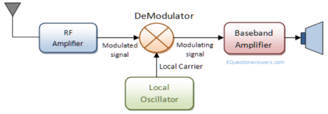
Fig: Demodulation
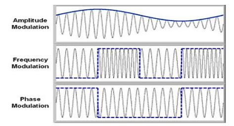
Fig: Demodulated Output
Q12) In a summing amplifier, if R = 1kΩ, Va = +3V, Vb = +8V, Vc = +9V, Vd = +5V and supply voltage is ±15V. Find the output voltage Vo.
A11) Vo = Sum of all input voltages applied at both the terminals
Vo = Va + Vb + Vc +Vd
Vo = -3 -8 +9 +5
Vo = +3V
Q13) Find the output voltage for the given circuit diagram if Rf = 5kΩ.
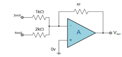
A12)
We know,
Gain (Av) = =
= 
Hence,
Av1 = 
Av2 = 
Now, Output voltage Vo = Sum of the two amplified input signals
Vo = Av1 x V1 + Av2 x V2
Vo =(-5 x 3) + ( -2.5x 4) mV
Vo = -25mV
As the above output voltage is negative hence it is an inverting amplifier.
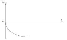
Q14) The integrator circuit as shown in the figure has R = 500K Ω and C=1µF. Find and plot the output voltage for the inputs as shown in the figure.
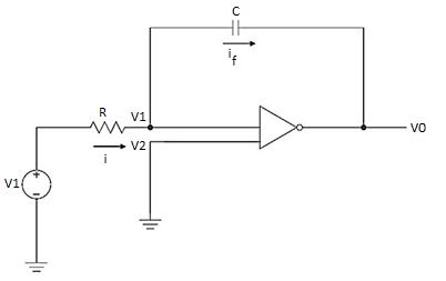
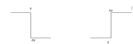
a) b)
c)vi= 2 sin 4tV d) vi= 4tV
A13)
We know that
v0 = - 1/RC  + v0(0)
Here R= 500K Ω and C = 1µF
1/RC = 1/ 500 x 1000 x 1 x 10-6
= 1/RC = 2
= -2  ; vi =- 5V
= -2 
= 10t V
Which means it is a ramp voltage with positive slope.
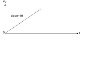
When vi=5V
-2  ; vi = 5V
= -2 
= -10t V
Which means it is a ramp voltage with negative slope.
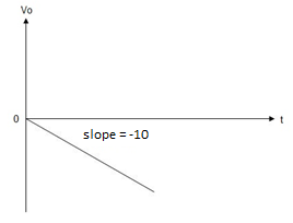
When vi= 2 sin4t V
Vo = -2 
= -4 [-cos 4t] /4 = cos 4t
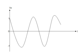
When vi=4t V
Vo = 
= -8 [t2/2] = - 4V
Q15) The VREF = VCC = 5 volts and the three resistors will be the same 10k ohms. So calculate the voltage at the A node. Assume Vout =0V and 5V.
A14)
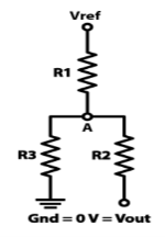
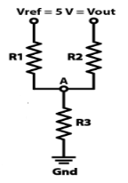
Vout = 0V

Va = 166V
Vout = 5V

Va = 333V
Q16) Draw the circuit and explain peak detector?
A15) Rectifier circuit gives average value of input signal; but in practice we need peak value of input signal. This is achieved by peak detector circuit. The following figure shows a simple peak detector circuit using diode and capacitor.
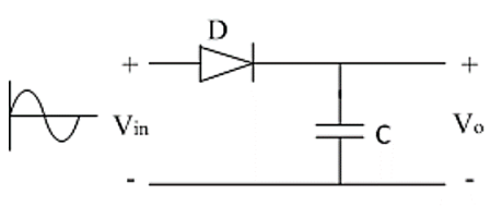
Fig: Peak detector
In the positive half cycle, diode D is forward biased and capacitor C starts charging. When input reaches its peak value, capacitor gets charged to positive peak value.
In negative half cycle, as input decreases, diode D is reversed biased and capacitor is isolated and holds the peak value of previous cycle. Hence called as peak detector.
But in practice, output is taken across some load RL, so when input voltage decreases capacitor discharges through load RL. To avoid this, select RL of very large value so that capacitor discharges very slowly hence almost hold the charge. Whatever charge it lost through RL is gets back in next half cycle.
Q17) Explain log amplifier?
A16) As the name says it is an amplifier which produces the output proportional to logarithmic of the applied input. The log amplifier using op-amp is shown below. The input is applied through the inverting end of op-amp. As the non-inverting end has voltage zero then by virtual ground concept the voltage at inverting terminal also becomes zero.
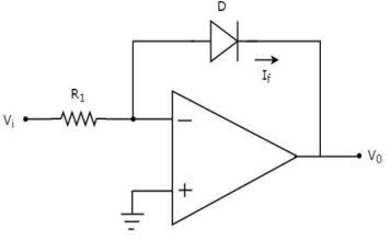
Fig: Log Amplifier
The equation for input voltage will be
 +If = 0
If = 
The current flowing through diode is given as

Where:
Is = Saturation Current
Vf = Voltage drop across diode in forward bias
VT = Thermal equivalent voltage
For feedback loop the KVL equation will be
0-Vf -V0 = 0
Vf = -V0
Substituting Vf in above equation of If

Equating both equations of If
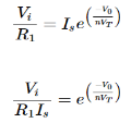
Taking natural log of both sides we get

The above equations shows that the output is natural log of the applied input.
Q18) Explain antilog amplifier?
A17) This device produces the output proportional to antilog of input. The inverting op-amp is used in this case as well. The figure below shows an antilog amplifier with its inverting terminal connected to the input end with diode and the non-inverting terminal is grounded.
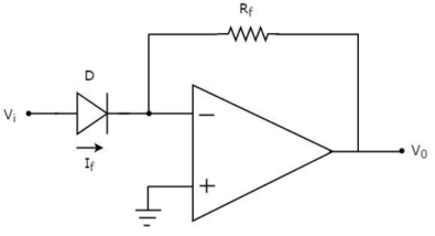
Fig: Antilog Amplifier
Applying KCL at input terminal we get


The current flowing through diode is given as

Substituting If in above voltage equation we get


At inverting terminal applying KVL we get


Substituting Vf in equation of V0 we get

The above equations shows that the output is natural antilog of the applied input.
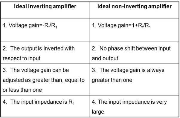
Q19) Explain the difference between inverting and non-inverting amplifier?
A18)
Q20) Draw the circuit of instrumentation amplifier having 3-op-amps?
A19) The Instrumentation amplifiers consist of three op-amps. In this circuit, a non-inverting amplifier is connected to each input of the differential amplifier.
This instrumentation amplifier provides high input impedance for exact measurement of input data from transducers. The circuit diagram of an instrumentation amplifier is as shown in the figure below.
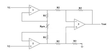
Fig: Instrumentation Amplifier
The op-amps 1 & 2 are non-inverting amplifiers and together form an input stage of the instrumentation amplifier. The op-amp 3 is a difference amplifier that forms the output stage of the instrumentation amplifier.
Working
The output stage of the instrumentation amplifier is a difference amplifier, whose output Vout is the amplified difference of the input signals applied to its input terminals.
If the outputs of op-amp 1 and op-amp 2 are Vo1 and Vo2 respectively, then the output of the difference amplifier is given by,
Vout = (R3/R2)(Vo1-Vo2)
The expressions for Vo1 and Vo2 can be found in terms of the input voltages and resistances.
Consider the input stage of the instrumentation amplifier as shown in the figure below.
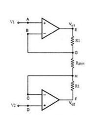
Fig: Input Stage of Instrumentation Amplifier
The potential at node A is the input voltage V1. Hence the potential at node B is also V1, from the virtual short concept. Thus, the potential at node G is also V1.
The potential at node D is the input voltage V2. Hence the potential at node C is also V2, from the virtual short. Thus, the potential at node H is also V2.
Ideally the current to the input stage op-amps is zero. Therefore, the current I through the resistors R1, Rgain and R1 remains the same.
Applying Ohm’s law between the nodes E and F,
I = (Vo1-Vo2)/(R1+Rgain+R1) ——————— 1
I = (Vo1-Vo2)/(2R1+Rgain)
Since no current is flowing to the input of the op-amps 1 & 2, the current I between the nodes G and H can be given as,
I = (VG-VH)/Rgain = (V1-V2)/Rgain ————————- 2
Equating equations 1 and 2,
(Vo1-Vo2)/(2R1+Rgain) = (V1-V2)/Rgain
(Vo1-Vo2) = (2R1+Rgain)(V1-V2)/Rgain —————— 3
The output of the difference amplifier is given as,
Vout = (R3/R2) (Vo1-Vo2)
Therefore, (Vo1 – Vo2) = (R2/R3)Vout
Substituting (Vo1 – Vo2) value in the equation 3, we get
(R2/R3)Vout = (2R1+Rgain)(V1-V2)/Rgain
i.e. Vout = (R3/R2){(2R1+Rgain)/Rgain}(V1-V2)
The above equation gives the output voltage of an instrumentation amplifier. The overall gain of the amplifier is given by the term (R3/R2) {(2R1+Rgain)/Rgain}.
Q21) List advantages of instrumentation amplifier?
A20) Advantages
- The gain of a three op-amp instrumentation amplifier circuit can be easily varied and controlled by adjusting the value of Rgain without changing the circuit structure.
- The gain of the amplifier depends only on the external resistors used. Hence, it is easy to set the gain accurately by choosing the resistor values carefully.
- The input impedance of the instrumentation amplifier is dependent on the non-inverting amplifier circuits in the input stage. The input impedance of a non-inverting amplifier is very high.
- The output impedance of the instrumentation amplifier is the output impedance of the difference amplifier, which is very low.
- The CMRR of the op-amp 3 is very high and almost all of the common mode signal will be rejected.
Q22) With the help of op-amp explain the circuit of zero crossing detector?
A21) An op-amp detector that has the ability to detect the change from positive to negative or negative to a positive level of a sinusoidal waveform is known as a zero- crossing detector.
It is also known to be a square wave generator as the applied input signal is converted into a square wave by the zero -crossing detector.
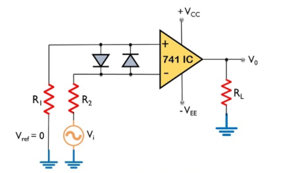
Fig: Zero crossing Detector
Here, the input signal Vi is provided to the inverting terminal of the op-amp while the non-inverting terminal is grounded by making use of two resistors R1 and R2.
It detects the point where the input signal crosses zero of the reference voltage level. For every crossing, the saturation level of the output signal changes from one to another.
The reference level is set at 0 and applied at the non-inverting terminal of the op-amp. The sine wave applied at the inverting terminal of the op-amp is compared with the reference level each time the phase of the wave changes either from positive to negative or negative to positive.
Firstly, when positive half of the sinusoidal signal appears at the input. Then the op-amp comparator compares the reference voltage level with the peak level of the applied signal.
Vo = Vref – Vi ---------------------------------------(1)
And we know the reference level is 0, thus
Vo = 0 – ( + Vsat) ----------------------------------------(2)
Therefore, Vo = - Vsat ---------------------------------(3)
During the negative half of the signal, thus the peak will have a negative polarity.
Again
Vo = Vref – Vi ---------------------------------------------(4)
Thus,
Vo = 0 - ( - Vsat) --------------------------------------------------(5)
So, we get
Vo = + Vsat ---------------------------------------------(6)
In this way, the zero -crossing detector detects the change in the level of the applied signal.
Zero crossing detector is also known to be a square wave generator. As the output of the window comparator is nothing but a square wave.
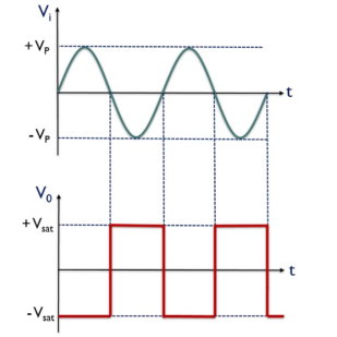
Fig 30 Input and output of zero crossing detector
V0 for the positive half of the applied signal is – Vsat,
This is the reason why we have achieved negative half of the square wave at the output when positive half of the sinusoidal signal is applied. While V0 for the negative half of the sinusoidal signal is + Vsat,
Applications:
- Phase Locked Loop
- Frequency counters and phase meters