Unit - 5
Digital Logic and basic circuit Design
Q1) Subtract 134 from 168.
A1) 168-134 = 168 + (-134)
Binary representation of 168= 1010 1000
Binary representation of 134= 1000 0110
Binary representation of -134= 0111 1001
[Because 1’s complement represents the negative magnitude of a binary number]
168 + (-134) = 1010 1000 + 0111 1001 = 10010 0001
As a carry bit is present, 1 will be added to the result and it represents that the result is positive. 0010 0001 + 1 = 0010 0010
Decimal representation of 0010 0010 is 34.
168-134=34; hence the result is correct.
Q2) Subtract 168 from 134.
A2) 134-168 = 134 + (-168)
Binary representation of 134= 1000 0110
Binary representation of 168= 1010 1000
Binary representation of -168= 0101 0111
[Because 1’s complement represents the negative magnitude of a binary number]
134 + (-168) = 1000 0110 + 0101 0111=1101 1101
As a carry bit is absent, 1’s complement of this value will be the final result and absence of carry bit represents that the result is negative.
1’s complement of 1101 1101 = 0010 0010
Decimal representation of 0010 0010 is 34.
As carry bit is absent the result is negative i.e -34 134 -168= -34; hence the result is correct.
Q3) Subtract 96 from 118.
A3) 118-96 = 118 + (-96)
Binary representation of 118= 0111 0110
Binary representation of 96= 0110 0000
Here 2’s complement represents the negative magnitude of a binary number.
Hence 2’s complement of 96 represents -96.
So -96= 1001 1111 118 + (-96) = 0111 0110 + 1001 1111=10001 0101
As a carry bit is present, 1 will be added to the result and presents of carry bit represents that the result is positive. 0001 0101+ 1= 0001 0110
Decimal representation of 0001 0110 is 22.
As carry bit is present the result is positive.
Q4) Subtract 118 from 96.
A4) 118-96 = 96 + (-118)
Binary representation of 96= 0110 0000
Binary representation of 118= 0111 0110
Here 2’s complement represents the negative magnitude of a binary number.
Hence 2’s complement of 118 represents -118.
So -118= 1000 1010 96 + (-118) = 0110 0000 + 1000 1010 1110 1010
As a carry bit is absent, 2’s complement of this value will be the final result and absence of carry bit represents that the result is negative.
2’s complement of 1110 1010 = 0001 0110
Decimal representation of 0001 0110 is 34. As carry bit is absent the result is negative i.e -34
Q5) Calculate the Decimal Equivalent of binary number 101112
A5) Calculating the Decimal Equivalent of binary number –
Step | Binary Number | Decimal Number |
Step 1 | 101012 | ((1 × 24) + (0 × 23) + (1 × 22) + (1 × 21) + (1 × 20))10 |
Step 2 | 101012 | (16 + 0 + 4 + 2 + 1)10 |
Step 3 | 101012 | 2310 |
Q6) Calculate Decimal Equivalent of 125758?
A6) Calculating Decimal Equivalent –
Step | Octal Number | Decimal Number |
Step 1 | 125758 | ((1 × 84) + (2 × 83) + (5 × 82) + (7 × 81) + (5 × 80))10 |
Step 2 | 125758 | (4096 + 1024 + 320 + 56 + 5)10 |
Step 3 | 125758 | 550010 |
Q7) Calculate Decimal equivalent of 19FDA16?
A7) Hexadecimal Number: 19FDA16
Calculating Decimal Equivalent –
Step | Hexadecimal Number | Decimal Number |
Step 1 | 19FDA16 | ((1 × 164) + (9 × 163) + (F × 162) + (D × 161) + (A × 160))10 |
Step 2 | 19FDA16 | ((1 × 164) + (9 × 163) + (15 × 162) + (13 × 161) + (10 × 160))10 |
Step 3 | 19FDA16 | (65536 + 36864 + 3840 + 208 + 10)10 |
Step 4 | 19FDA16 | 10645810 |
Q8) Calculate Binary Equivalent of 2710?
A8) Decimal Number: 2710
Calculating Binary Equivalent –
Step | Operation | Result | Remainder |
Step 1 | 27 / 2 | 13 | 1 |
Step 2 | 13 / 2 | 6 | 1 |
Step 3 | 6 / 2 | 3 | 0 |
Step 4 | 3 / 2 | 1 | 1 |
Step 5 | 1 / 2 | 0 | 1 |
Hence, the remainders are arranged in the reverse order and we get:
Decimal Number − 2710 = Binary Number − 110112.
Q9) Calculate Decimal Equivalent of 111102
A9) Binary Number − 111102
Calculating Decimal Equivalent –
Step | Binary Number | Decimal Number |
Step 1 | 111102 | ((1 × 24) + (1 × 23) + (1 × 22) + (1 × 21) + (0 × 20))10 |
Step 2 | 111102 | (16 + 8 + 4 + 2 + 0)10 |
Step 3 | 111102 | 3010 |
Binary Number − 111102 = Decimal Number − 3010
Q10) Calculate Binary equivalent of 268?
A10) Octal Number − 268
Calculating its Binary Equivalent −
Step 1 – Converting octal to Decimal
Step | Octal Number | Decimal Number |
Step 1 | 268 | ((2 × 81) + (6 × 80))10 |
Step 2 | 268 | (16 + 6 )10 |
Step 3 | 268 | 2210 |
Octal Number − 268 = Decimal Number − 2210
Step 2 − Converting Decimal to Binary
Step | Operation | Result | Remainder |
Step 1 | 22 / 2 | 11 | 0 |
Step 2 | 11 / 2 | 5 | 1 |
Step 3 | 5 / 2 | 2 | 1 |
Step 4 | 2 / 2 | 1 | 0 |
Step 5 | 1 / 2 | 0 | 1 |
Decimal Number − 2210 = Binary Number − 101102
Octal Number − 268 = Binary Number − 101102
Q11) Find octal equivalent of 101012
A11) Binary Number − 101012
Its Octal Equivalent –
Step | Binary Number | Octal Number |
Step 1 | 101012 | 010 101 |
Step 2 | 101012 | 28 58 |
Step 3 | 101012 | 258 |
Binary Number − 101012 = Octal Number − 258
Q12) Find binary equivalent of 258
A12) Octal Number − 258
Its Binary Equivalent –
Step | Octal Number | Binary Number |
Step 1 | 258 | 210 510 |
Step 2 | 258 | 0102 1012 |
Step 3 | 258 | 0101012 |
Octal Number − 258 = Binary Number − 101012
Q13) Find hexadecimal equivalent of 101012
A13) Binary Number − 101012
Its hexadecimal Equivalent –
Step | Binary Number | Hexadecimal Number |
Step 1 | 101012 | 0001 0101 |
Step 2 | 101012 | 110 510 |
Step 3 | 101012 | 1516 |
Binary Number − 101012 = Hexadecimal Number − 1516
Q14) Find binary equivalent of 1516
A14) Hexadecimal Number − 1516
Its Binary Equivalent –
Step | Hexadecimal Number | Binary Number |
Step 1 | 1516 | 110 510 |
Step 2 | 1516 | 00012 01012 |
Step 3 | 1516 | 000101012 |
Hexadecimal Number − 1516 = Binary Number − 101012
Q15) Simplify the Boolean function, f = p’qr + pq’r + pqr’ + pqr
A15) Using the Boolean postulate, x + x = x.
Hence, we can write the last term pqr two more times.
⇒ f = p’qr + pq’r + pqr’ + pqr + pqr + pqr
Now using the Distributive law for 1st and 4th terms, 2nd and 5th terms, 3rdand 6th terms we get.
⇒ f = qr(p’ + p) + pr(q’ + q) + pq(r’ + r)
Using Boolean postulate, x + x’ = 1 and x.1 = x for further simplification.
⇒ f = qr(1) + pr(1) + pq(1)
⇒ f = qr + pr + pq
⇒ f = pq + qr + pr
Therefore, the simplified Boolean function is f = pq + qr + pr.
Hence, we got two different Boolean functions after simplification of the given Boolean function. Functionally, these two functions are same. As per requirement, we can choose one of them.
Q16) Find the complement of the Boolean function,
f = p’q + pq’.
A16) Using DeMorgan’s theorem, (x + y)’ = x’.y’ we get
⇒ f’ = (p’q)’.(pq’)’
Then by second law, (x.y)’ = x’ + y’ we get
⇒ f’ = {(p’)’ + q’}.{p’ + (q’)’}
Then by using, (x’)’=x we get
⇒ f’ = {p + q’}.{p’ + q}
⇒ f’ = pp’ + pq + p’q’ + qq’
Using x.x’=0 we get
⇒ f = 0 + pq + p’q’ + 0
⇒ f = pq + p’q’
Therefore, the complement of Boolean function, p’q + pq’ is pq + p’q’.
Q17) Using Boolean algebra techniques, simplify this expression: AB + A(B + C) + B(B + C)
A17)
Step 1: Apply the distributive law to the second and third terms in the expression, as follows: AB + AB + AC + BB + BC
Step 2: Apply rule 7 (BB = B) to the fourth term. AB + AB + AC + B + BC
Step 3: Apply rule 5 (AB + AB = AB) to the first two terms. AB + AC + B + BC
Step 4: Apply rule 10 (B + BC = B) to the last two terms. AB + AC + B
Step 5: Apply rule 10 (AB + B = B) to the first and third terms. B+AC At this point the expression is simplified as much as possible.

Fig: Implementation using gates
Q18) Design a logic circuit that has three inputs, A, B, and C, and whose output will be HIGH only when a majority of the inputs are HIGH.
A18)
Step 1. Set up the truth table. On the basis of the problem statement, the output x should be 1 whenever two or more inputs are 1; for all other cases, the output should be 0
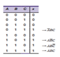
Fig: Truth Table with AND terms
Step 2. Write the AND term for each case where the output is a 1. There are four such cases. The AND terms are shown next to the truth table. Again, note that each AND term contains each input variable in either inverted or noninverted form.
Step 3. Write the sum-of-products expression for the output. x =  BC + A
 C + AB
 + ABC
+ ABC
Step 4. Simplify the output expression.
This expression can be simplified in several ways. Perhaps the quickest way is to realize that the last term ABC has two variables in common with each of the other terms. Thus, we can use the ABC term to pair with each of the other terms. The expression is rewritten with the ABC term occurring three times:
x =  BC + A
 C + AB
 + ABC + ABC + ABC
Factoring the appropriate pairs of terms, we ha
x = BC ( + A) + AC (
 + B) + AB (
 + C) Each term in parentheses is equal to 1, so we have x = BC + AC + AB
Step 5. Implement the circuit for the final expression. This expression is implemented in Figure. Since the expression is in SOP form, the circuit consists of a group of AND gates working into a single OR gate.
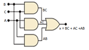
Fig: Implementation using gates
Q19) Draw IR transmitter and receiver circuit?
A19) The most commonly used wireless technology is the IR communication. This technology is employed in remotes mostly of TV and AC. The receiver senses the modulated IR pulse and converts it into electrical signal. The receiver is TSOP1738 which is generally used. The IR LED are used as transmitters. Below we will study in detail with the circuit diagram and working.
As we know that the IR light is not visible through naked eyes as they are beyond the visible range. Although they are above the visible light range but has few qualities like polarization, reflection which helps in wireless technology.
IR Transmitter
Here Astable multivibrator is used to produce oscillating frequency. The multivibrator is made out of IC 555 timer. The circuit generates output frequency of around 38kHz which is accomplished by circuit elements R1=1k , R2=20k
 and capacitor of 1nF.
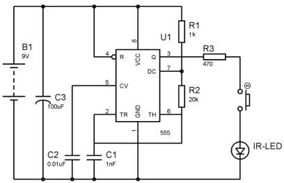
Fig IR Transmitter
The output is taken from pin 3 which is connected to 470 resistor and a push button switch. The circuit produces modulated IR signal of 38kHz approx. Whenever the push button is pressed.
IR Receiver
Here TSOP1738 output is connected to the LED. A transistor Q1 which is PNP transistor is used which turns off when output from TSOP is high. Whenever IR is detected the output of it goes low and this turns ON the LED. When output from TSOP is high the transistor acts as open circuit and LED is turned OFF. The 10k resistor is used for providing proper biasing to the transistor. The 470 resistor is used to limit the current at LED.
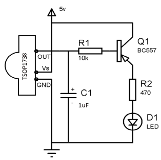
Fig IR Receiver
Q20) Explain the types of relay driver circuit with diagram?
A20) A circuit which can drive a relay is called relay driver circuit. This circuit acts as switch which open and close as per the requirement of the circuit. The relay driver can be of following types
DC Relay Driver Circuit
In these circuits the relay behaves as an inductor. In many devices when there is voltage spike the current in the coil is suddenly interrupted and a large voltage is produced across it producing large amount of current. This huge amount of current can damage the near by devices. To overcome this, we use diode with the DC relay circuit.
The DC relay driver circuit has mainly three components DC relay, Zener Diode and DC voltage source.
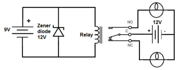
Fig DC Relay Circuit
The Zener diode is connected in reverse bias in the circuit. Supply of 9V is used and the Zener diode is connected in parallel with the relay. All the excess power is shunt to ground once a certain threshold is reached.
AC Relay Driver Circuit
This relay runs on AC power. For instance, if we need 110V from an AC power we require 110V ac supply. A capacitor and resistor in series are connected which acts as transient voltage suppressor. Relay driver serves as the first half of the relay driver. When there is sufficient power in relay it will turn on and will power to load to which it is connected.
Generic Relay Circuit
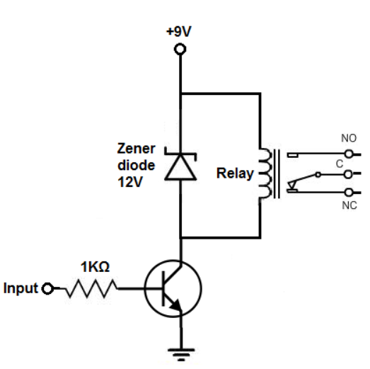
Fig Relay Driver
The circuit which can be driven by both ac and dc input voltage are called generic relay circuits. A transistor is used to drive the relay which uses less power. As transistor acts as an amplifier the base of the transistor should be supplied with enough current such that proper amount of current flows from emitter to the collector. Now the transistor starts conducting.
With no voltage or input current applied to the transistor's base lead, the transistor's emitter-to-collector channel is open, hence blocking current flow through the relay's coil. However, if sufficient voltage and input current are applied to the base lead, the transistor's emitter-to-collector channel will close, allowing current to flow through the relay's coil.
Q21) Draw and explain with the astable multivibrator a square wave oscillation?
A21) The astable multivibrator shown in the figure below [Ref.1] can be used to generate square wave oscillations. The diode is connected across RB and the diode and capacitor are charged through RA to a voltage of 2/3 of VCC. The capacitor discharges through RB and Q1. The discharging of capacitor when reaches 1/3VCC the discharging stops.

Fig: Astable multivibrator as square wave oscillator
Square wave Oscillation using Monostable Multivibrator
It also called one shot, operates by charging a timing capacitor with a current set by external resistance. When the one shot is triggered, the charging network cycles only once during the timing interval. The total timing interval includes the recovery time needed for the capacitor to charge up to the threshold level.
When Vcc high is applied to the trigger input, the trigger comparator output is low, the flip flop output is high, the transistor is on, the timing capacitor is discharged to ground potential. The output of the 555 circuit is low.

Fig: Monostable multivibrator
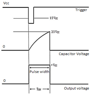
Fig: Output waveform
When negative voltage is applied to the trigger input, output of trigger comparator goes high. When trigger pulse drops below 1/3 Vcc output of flip flop goes low, output of 555 circuit goes high and the transistor turns off
Q22) Using op-amp fixed frequency generator?
A22) This means there will be no stable level at the output. So, the output will be swinging between high and low. This character of unstable output is used as a clock or square wave output for many applications.
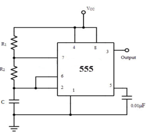
Fig: Astable Multivibrator
It is self-triggered multivibrator as pin 2 and 6 are connected. The supply is given through pin 8 and the output is obtained through pin 3. The timer will be reset if a low signal is given to pin 4. The capacitor is connected across pin 5 so that the external noise or any dc level are filtered. The resistor pair R1 and R2 form a circuit for determining the width of the output pulse.
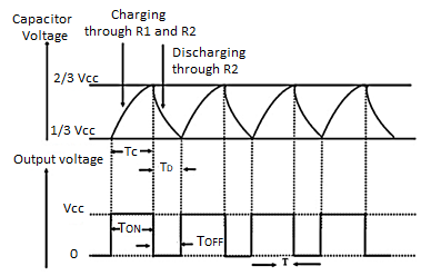
Fig: Capacitor and Output voltage waveform
During charging the capacitor charges through R1 and R2 and voltage across capacitor rises exponentially and during discharging the capacitor discharges through R2 and voltage falls exponentially. The output is obtained across pin 3.
The time for which capacitor charges from 1/3VCC to 2/3VCC is equal to the time the output is high which is given by
tc= 0.69(R1+R2) C
The discharging time from 2/3Vcc to 1/3VCC is given as
td= 0.69 R2C
The total period of output waveform is given by
T = tc+ td = 0.69(R1+2R2) C
The frequency of oscillations is given by
f0 =  =
= 
The duty cycle is defined as the ratio of the charging time of capacitor at which the output is high to the total time period.
%duty cycle =  x 100
x 100
Q23) Draw and explain the LED Drive circuit with proper diagram?
A23) Circuit configurations that may be used to convert the information voltage signal at the transmitter into a modulation current suitable for an LED source. LED drive circuits are typically designed to control the current running through a string of LEDs independent of the voltage drop across the LED string.
Digital transmission:
- The operation of the LED for binary digital transmission requires the switching on and off of a current in the range of several tens to several hundreds of milli-amperes.
- This must be performed at high speed in response to logic voltage levels at the driving circuit input. A common method of achieving this current switching operation for an LED is shown in Figure
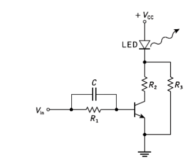
- The circuit illustrated uses a bipolar transistor switch operated in the common emitter mode.
- This single-stage circuit provides current gain as well as giving only a small voltage drop across the switch when the transmitter is in saturation.
- The maximum current flow through the LED is limited by the resistor R2 while independent bias to the device may be provided by the incorporation of resistor R3.
- The switching speed of the common emitter configuration is limited by space charge and diffusion capacitance; thus bandwidth is traded for current gain.
- This may be compensated by overdriving (pre-emphasizing) the base current during the switch-on period. In the circuit shown in Figure pre-emphasis is accomplished by use of the speed-up capacitor C.
Low-impedance drive circuit:
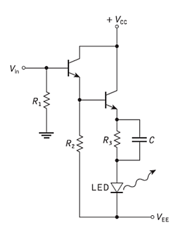
- Increased switching speed may be obtained from an LED without a pulse shaping or speed-up element by use of a low-impedance driving circuit, whereby charging of the space charge and diffusion capacitance occurs as rapidly as possible.
- This may be achieved with the emitter follower drive circuit shown in Figure.
- The use of this configuration with a compensating matching network (R3C) provides fast direct modulation of LEDs with relatively low drive power.
- A circuit, with optimum values for the matching network, is capable of giving optical rise times of 2.5 ns for LEDs with capacitance of 180 pF, thus allowing 100 Mbit s−1 operations.
Q24) Explain transistor as an amplifier. Also explain how it acts as a single stage amplifier?
A24) Transistor raises the strength of a weak signal and hence acts an amplifier. The transistor amplifier circuit is shown in the figure below.

Figure. Transistor as an Amplifier
The transistor has three terminals namely emitter, base and collector. The emitter and base of the transistor are connected in forward biased and the collector base region is in reverse bias. The forward bias means the P-region of the transistor is connected to the positive terminal of the supply and the negative region is connected to the N-terminal and in reverse bias just opposite of it has occurred.
Vee is applied to the input circuit along with the input signal to achieve the amplification. The DC voltage VEE keeps the emitter-base junction under the forward biased condition regardless of the polarity of the input signal and is known as bias voltage.
When a weak signal is applied to the input, a small change in signal voltage causes a change in emitter current this change is almost the same in collector current because of the transmitter action.
In the collector circuit, a load resistor RC of high value is connected. When collector current flows through such a high resistance, it produces a large voltage drop across it. Thus, a weak signal (0.1V) applied to the input circuit appears in the amplified form (10V) in the collector circuit.
Input Resistance
When the input circuit is forward biased, the input resistance will be low. The input resistance is the opposition offered by the base-emitter junction to the signal flow.
Hence, it is the ratio of small change in base-emitter voltage (ΔVBE) to the resulting change in base current (ΔIB) at constant collector-emitter voltage.
Input resistance, Ri=ΔVBE/ΔIb
Where Ri = input resistance, VBE = base-emitter voltage, and IB = base current.
Output Resistance
The output resistance of a transistor amplifier is very high. The collector current changes very slightly with the change in collector-emitter voltage.
The ratio of change in collector-emitter voltage (ΔVCE) to the resulting change in collector current (ΔIC) at constant base current.
Output resistance = Ro=ΔVCE/ΔIC
Where Ro = Output resistance, VCE = Collector-emitter voltage, and IC = Collector-emitter voltage.
Current gain
It is the ratio of change in collector current (ΔIC) to the change in base current (ΔIB).
Current gain, β=ΔIC/ ΔIB
Voltage Gain
It is the ratio of change in output voltage (ΔVCE) to the change in input voltage (ΔVBE).
Voltage gain, AV=ΔVCE/ΔVBE

Power Gain
It is the ratio of output signal power to the input signal power.
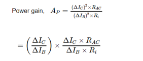
= current gain x voltage gain
Q25) What are universal gates. Draw their symbol and truth tables?
A25) Universal gates
- NAND & NOR gates are known as universal gates.
- We can implement any Boolean function by using NAND gates and NOR gates alone.
NAND gate
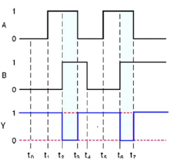
It is a digital circuit which has two or more inputs and single output and it is the inversion of logical AND gate.
The truth table of 2-input NAND gate is:
A | B | Y = (A.B)’ |
0 | 0 | 1 |
0 | 1 | 1 |
1 | 0 | 1 |
1 | 1 | 0 |
Here A, B are the inputs and Y is the output of two input NAND gate. When both inputs are ‘1’, then the output, Y is ‘0’. If at least one of the input is zero, then the output, Y is ‘1’. This is just the inverse of AND operation.
The image shows the symbol of NAND gate:

Fig.: NAND gate
NAND gate works same as AND gate followed by an inverter.
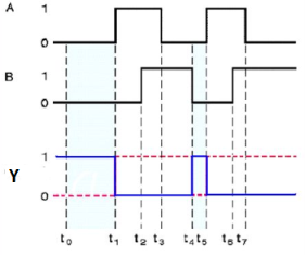
Timing Diagram:
NOR gate
It is a digital circuit that has two or more inputs and a single output which is the inversion of logical OR of all inputs.
The truth table of 2-input NOR gate is:
A | B | Y = (A+B)’ |
0 | 0 | 1 |
0 | 1 | 0 |
1 | 0 | 0 |
1 | 1 | 0 |
Here A and B are the two inputs and Y is the output. If both inputs are ‘0’, then the output is ‘1’. If any one of the input is ‘1’, then the output is ‘0’. This is exactly opposite to two input OR gate operation.
The symbol of NOR gate is:

Fig.: NOR gate (ref. 1)
NOR gate works exactly same as that of OR gate followed by an inverter.
Timing Diagram:
