Unit - 5
Linear & Nonlinear applications of op-amp
Q1) Explain the idealised analysis of op-amp circuits?
A1)
An Operational Amplifier is basically a three-terminal device which consists of two high impedance inputs. One of the inputs is called the Inverting Input, marked with a negative or “minus” sign, ( – ). The other input is called the Non-inverting Input, marked with a positive or “plus” sign ( + ).
A third terminal represents the operational amplifiers output port which can both sink and source either a voltage or a current.
In a linear operational amplifier, the output signal is the amplification factor, known as the amplifiers gain ( A ) multiplied by the value of the input signal and depending on the nature of these input and output signals, there can be four different classifications of operational amplifier gain.
- Voltage – Voltage “in” and Voltage “out”
- Current – Current “in” and Current “out”
- Transconductance – Voltage “in” and Current “out”
- Transresistance – Current “in” and Voltage “out”
Q2) Explain the important characteristics of op-amp?
A2)
Open Loop Gain (Avo)
The main function of an operational amplifier is to amplify the input signal and the more open loop gain it has the better. Open-loop gain is the gain of the op-amp without positive or negative feedback and for such an amplifier the gain will be infinite
Input impedance (ZIN)
Input impedance is the ratio of input voltage to input current and is assumed to be infinite to prevent any current flowing from the source supply into the amplifiers input circuitry ( IIN = 0 ). Real op-amps have input leakage currents from a few pico-amps to a few milli-amps.
Output impedance (ZOUT)
The output impedance of the ideal operational amplifier is assumed to be zero acting as a perfect internal voltage source with no internal resistance so that it can supply as much current as necessary to the load.
This internal resistance is effectively in series with the load thereby reducing the output voltage available to the load. Real op-amps have output impedances in the 100-20kΩ range.
Bandwidth (BW)
An ideal operational amplifier has an infinite frequency response and can amplify any frequency signal from DC to the highest AC frequencies, so it is therefore assumed to have an infinite bandwidth.
With real op-amps, the bandwidth is limited by the Gain-Bandwidth product (GB), which is equal to the frequency where the amplifiers gain becomes unity.
Offset Voltage (VIO)
The amplifiers output will be zero when the voltage difference between the inverting and the non-inverting inputs is zero, the same or when both inputs are grounded. Real op-amps have some amount of output offset voltage.
Q3) Explain inverting and non-inverting amplifier?
A3)
Inverting Amplifier

The input signal vi is applied to the inverting input terminal through resistor R1 and non-inverting input terminal is grounded. The feedback from the output of the inverting terminal is provided through the feedback resistor Rf.
Since the input is applied to the inverting terminal vo and vi are opposite in polarity and hence the feedback is negative. Since the non-inverting input terminal is grounded v2=0. Due to virtual short at the input of op-amp the inverting and non-inverting input terminals are at the same potential.
Therefore, v1 = v2 = 0.
Due to high input impedance of Op-amp the current flowing into its inverting input terminal is zero. Therefore, the same current flows through R1 and Rf .
i 1 = i f
But i1 = vi – v1 / R1 = vi/R1
i f = v1 – vo / Rf = -vo/Rf
Vi/R1 = - vo/Rf
Af = vo/vi = -Rf/R1
Af is the closed loop voltage gain or voltage gain with negative feedback.
Non-inverting amplifier
Non- Inverting amplifier is one in which the output is in phase with respect to input that is if you apply a positive voltage, output will be positive. The output is an non -inverted amplified version of input.

Assuming the op-amp is ideal and applying the concept of virtual short, the voltage at the inverting terminal is equal to non- inverting terminal.
Applying KCL at inverting node we get
Vi -Vo/ R2 + Vo – 0 / R1 = 0
By rearranging the terms, we will get
Voltage gain Av = Vo/ Vi = (1+ Rf/Ri)
Gain of non- inverting amplifier Av= (1+ Rf/Ri).
Q4) Explain differential amplifier?
A4)
The differential amplifier amplifies the difference between two voltages making this type of operational amplifier circuit a Subtractor This type of operational amplifier circuit is commonly known as a Differential Amplifier.

By connecting each input in turn to 0v ground we can use superposition to solve for the output voltage Vout. Then the transfer function for a Differential Amplifier circuit is given as:
I1 = V1-Va/R1 ; I2 = V2-Vb/R2 ; If = Va –(Vout)/R3
Summing Point Va =Vb
Vb = V2(R4/R2+R4)
If V2 =0 then Vout = -V1 (R3/R1)
If V1=0 then Vout = V2(R4/R2+R4)(R1+R3/R1)
Vout = -Vout (a) + Vout(b)
Vout = -V1(R3/R1) + V2(R4/R2+R4)(R1+R3/R1)
When resistors, R1 = R2 and R3 = R4 the above transfer function for the differential amplifier can be simplified to the following expression:
Vout = (V2 -V1)
The output is the difference between the two inputs hence, the op-amp can be used as subtractor.
Q5) Explain instrumentation amplifier?
A5)
The Instrumentation amplifiers consist of three op-amps. In this circuit, a non-inverting amplifier is connected to each input of the differential amplifier.
This instrumentation amplifier provides high input impedance for exact measurement of input data from transducers. The circuit diagram of an instrumentation amplifier is as shown in the figure below.

The op-amps 1 & 2 are non-inverting amplifiers and together form an input stage of the instrumentation amplifier. The op-amp 3 is a difference amplifier that forms the output stage of the instrumentation amplifier.
Working
The output stage of the instrumentation amplifier is a difference amplifier, whose output Vout is the amplified difference of the input signals applied to its input terminals.
If the outputs of op-amp 1 and op-amp 2 are Vo1 and Vo2 respectively, then the output of the difference amplifier is given by,
Vout = (R3/R2)(Vo1-Vo2)
The expressions for Vo1 and Vo2 can be found in terms of the input voltages and resistances.
Consider the input stage of the instrumentation amplifier as shown in the figure below.

The potential at node A is the input voltage V1. Hence the potential at node B is also V1, from the virtual short concept. Thus, the potential at node G is also V1.
The potential at node D is the input voltage V2. Hence the potential at node C is also V2, from the virtual short. Thus, the potential at node H is also V2.
Ideally the current to the input stage op-amps is zero. Therefore, the current I through the resistors R1, Rgain and R1 remains the same.
Applying Ohm’s law between the nodes E and F,
I = (Vo1-Vo2)/(R1+Rgain+R1) ——————— 1
I = (Vo1-Vo2)/(2R1+Rgain)
Since no current is flowing to the input of the op-amps 1 & 2, the current I between the nodes G and H can be given as,
I = (VG-VH)/Rgain = (V1-V2)/Rgain ————————- 2
Equating equations 1 and 2,
(Vo1-Vo2)/(2R1+Rgain) = (V1-V2)/Rgain
(Vo1-Vo2) = (2R1+Rgain)(V1-V2)/Rgain —————— 3
The output of the difference amplifier is given as,
Vout = (R3/R2) (Vo1-Vo2)
Therefore, (Vo1 – Vo2) = (R2/R3)Vout
Substituting (Vo1 – Vo2) value in the equation 3, we get
(R2/R3)Vout = (2R1+Rgain)(V1-V2)/Rgain
i.e. Vout = (R3/R2){(2R1+Rgain)/Rgain}(V1-V2)
The above equation gives the output voltage of an instrumentation amplifier. The overall gain of the amplifier is given by the term (R3/R2){(2R1+Rgain)/Rgain}.
Q6) Write a short note on active filters?
A6)
Active filters are the electronic circuits, which consist of active element like op-amp(s) along with passive elements like resistor(s) and capacitor(s).
Active filters are mainly classified into the following four types based on the band of frequencies that they are allowing and / or rejecting −
- Active Low Pass Filter
- Active High Pass Filter
- Active Band Pass Filter
- Active Band Stop Filter
Q7) Explain P controller?
A7)
P Control
The Output power is directly proportional to control error. The higher the proportion coefficient, the less the output power at the same control error
Proportional control is mainly for fast-response systems with a large transmission coefficient. To adjust the proportional controller first set the maximum proportion coefficient where in the output power decreases to zero.
When the measured value is stabilized, set a specified value and gradually reduce the proportion coefficient and the control error will decrease.
If there are periodic oscillations in the system, the proportion coefficient should be increased so that control error is minimal periodic oscillations decrease to the limit.
Q8) Explain PI control?
A8)
The Output power equals to the sum of proportion and integration coefficients. The higher the proportion coefficient, the less the output power at the same control error. The higher the integration coefficient, the slower the accumulated integration coefficient.
PI control provides zero control error and and is insensitive to interference of the measurement channel. The PI control disadvantage is slow reaction to disturbances.
To adjust the PI controller first set the integration time equal to zero, and the maximum proportion time. Then by decreasing the coefficient of proportionality, achieve periodic oscillations in the system.
Q9) Explain PID control?
A9)
The Output power equals to the sum of three coefficients: proportional, integral and differential. The higher the proportion coefficient, the less the output power at the same control error.
The higher the integration coefficient, the slower the accumulated integration coefficient. The higher the differentiation coefficient, the greater the response of the system to the disturbance.
The PID controller is used in inertial systems with relatively low noise level of the measuring channel.
The advantage of PID is fast warm up time, accurate setpoint temperature control and fast reaction to disturbances.
Q10) Explain lead/lag compensator using op-amp
A10)
Lag compensator
A lag compensator is one which adds a pole to the system and is used to improve the steady state response of the system. A lag compensator provides phase lag negative phase in the frequency response of system.
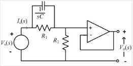
Using the concept of virtual ground, the op-amp lag compensator can be redrawn as shown in the figure
Using voltage divider principle, the transfer function of the system is
Vo/Vs =(1+s*C*R1)/(1+(R1+R2)*s*C),
Hence the phase added to system is given as
Ω = tan-1(ω*C*R1) – tan-1(ω*C*(R1+R2))
Since R1<R1+R2 and tan-1(x) is increasing function (if a <b, tan-1(a)< tan1(b)) Ω is negative phase lag.
Lead compensator
A lead compensator is one which adds a zero the system and is used to improve the transient response of the system. A lead compensator provides phase lead positive phas) in the frequency response of system

Using the concept of virtual ground, the op-amp lag compensator can be redrawn as shown in the figure
Using voltage divider principle, the transfer function of the system is
Vo/Vs=(1+s*C*R1)/(1+(R1*R2/(R1+R2))*s*C),
Hence the phase added to system is given as
Ω =tan-1(ω*C*R1) -tan-1(ω*C*R1*R2/(R1+R2)).
Since R1 > R1*R2/(R1+R2) Ω is positive(phase lead).
Q11) Explain integrator using op-amp?
A11)

Since the non-inverting input terminal of op-amp is grounded v2=0. Due to virtual short at the input of op-amp the inverting and non-inverting input terminals are at the same potential
Therefore v1=v2=0
Due to high impedance of op-amp the current flowing into its input terminal is zero. Therefore the same current flows through R and C
That is
i1 = if -------------------(1)
Where i1 = vi – v1 /R = vi -/R---------------------(2)
And if = C d/dt[v1 – v0] = -C dv0/dt --------------------(3)
Substituting (2) and (3) in (1) we get
Vi = - C/R dv0/dt ------------------------(4)
Dvo/dt = (-1/RC) vi ---------------------------- (5)
Integrating both sides of eq(5) we get
v0 = - 1/RC  + v0(0) --------------------------(6)
Where v0(0) is the initial voltage on the capacitor at t=0.
Note: v0(o) represents the constant of integration.
From eq(6) we find that the output voltage is proportional to the integral of the input voltage.
Therefore v0 = - 1/RC 

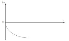
Q12) The integrator circuit as shown in the figure has R = 500K Ω and C=1µF. Find and plot the output voltage for the inputs as shown in the figure.

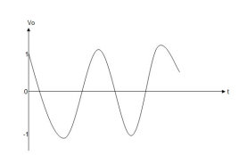
c)vi= 2 sin 4tVd) vi= 4tV
A12)
We know that
v0 = - 1/RC  + v0(0)
Here R= 500K Ω and C = 1µF
1/RC = 1/ 500 x 1000 x 1 x 10-6
= 1/RC = 2
= -2  ; vi =- 5V
= -2 
= 10t V
Which means it is a ramp voltage with positive slope.

When vi=5V
-2  ; vi = 5V
= -2 
= -10t V
Which means it is a ramp voltage with negative slope.

When vi= 2 sin4t V
Vo = -2 
= -4 [-cos 4t] /4 cos 4t

When vi=4t V
Vo = 
= -8 [t2/2]
= - 4V
Q13) Explain the working of regulator?
A13)
By utilizing an op-amp and few other external components, linear voltage regulator is built The same circuit is also a voltage stabilizer, able to stabilize voltage at a grade better than The transistor is used to supply the load with much more current than the op-amp itself could possibly supply.
The D1 diode is a Zener -type diode and it is used for voltage reference.
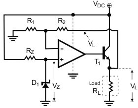
Fig. Basic op-amp voltage regulator
D1 is biased through Rz. When correctly reserve biased, the Zener diode keeps the voltage across its leads close to the Zener breakdown voltage. The op-amp is used as a linear voltage amplifier.
Due to the high open loop voltage gain of the op-amp the op-amp remains in its linear region, the voltage difference between its inverting (V-) and non-inverting input (V+) is almost equal to zero.
In other words, the voltage at its non-inverting input, in respect to the ground, equals the voltage at its inverting input:
V-=V+ -------(1)
Equation (1) holds true for any op-amp working at its linear region (as an amplifier).
R1 and R2 form a voltage divider, and the voltage (V-) at their connection point is also given by the well- known voltage-divider formula:
V-=VL·R1/(R1+R2) ------ (2)
However, V+ is also equal to the Zener breakdown voltage (Vz), because the non-inverting input of the op-amp is directly connected to the cathode of the Zener diode.
V+=VZ -----------------(3)
After solving (1),(2) and (3), we get:
VL=VZ·(1+R2/R1) --------------(4)
From equation (4), we conclude that VL voltage which is the voltage applied to the load is directly proportional to the Zener voltage.
As long as Zener voltage remains stable, VL also remains stable. Additionally, the voltage applied to the load, can be easily adjusted by adjusting R1, R2 or both. For continues voltage adjustment, R1 and R2 can be replaced by a potentiometer, having its wiper at the non-inverting input of the op-amp, and its other leads at the ground and the VL line, respectively.
Q14) Explain Wein bridge oscillator?
A14)
Wien bridge oscillator is an audio frequency sine wave oscillator of high stability and simplicity. The feedback signal in this circuit is connected to the non-inverting input terminal so that the op-amp is working as a non-inverting amplifier.
The feedback network does not provide any phase shift. The circuit can be viewed as a Wien bridge with a series combination of R1 and C1 in one arm and parallel combination of R2 and C2 in the adjoining arm. Resistors R3 and R4 are connected in the remaining two arms.
The condition of zero phase shift around the circuit is achieved by balancing the bridge. The series and parallel combination of RC network form a lead-lag circuit.
At high frequencies, the reactance of capacitor C1 and C2 approaches zero. This causes C1 and C2 appears short. Here, capacitor C2 shorts the resistor R2. Hence, the output voltage Vo will be zero since output is taken across R2 and C2 combination. So, at high frequencies, circuit acts as a 'lag circuit'.
At low frequencies, both capacitors act as open because capacitor offers very high reactance. Again, output voltage will be zero because the input signal is dropped across the R1 and C1 combination. Here, the circuit acts like a 'lead circuit'.
But at one particular frequency between the two extremes, the output voltage reaches to the maximum value. At this frequency only, resistance value becomes equal to capacitive reactance and gives maximum output. Hence, this frequency is known as oscillating frequency (f).


Consider the feedback circuit, on applying voltage divider rule
Vf(s) = Vo(s) x Zp(s)/ Zp(s) + Zs(s)
Zs(s) = R1 + 1/sC1 and Zp(s) = R2|| 1/sC2
Let R1=R2=R and C1=C2=C . On solving
β = Vf(s)/ Vo(s) = RsC /(RsC) 2 + 3RsC + 1 ---------------------------(1)
Since the op-amp is operated in the non-inverting configuration the voltage gain
Av = Vo(s)/ Vf(s) = 1 + R3/R4 -------------------(2)
Applying the condition for sustained oscillations, = Av β =1
RsC /(RsC) 2 + 3RsC + 1. 1 + R3/R4
S=jw
(1 + R3/R4) ( jwRC/ - R2 C2 w2 + 3 jwRC + 1) =1
Jw RC (1 + R3/R4)= (- R2 C2 w2 + 3 jwRC + 1)
Jw[(1 + R3/R4)RC – 3RC] = 1- R2 C2 w2
To obtain the frequency of oscillation equate the real part to zero
1 - R2 C2 w2 = 0
w = 1/RC
f = 1/ 2 π RC
To obtain the condition for gain at the frequency of oscillation equate the imaginary part to zero.
Jw[(1 + R3/R4)RC – 3RC] = 0
jw[(1 + R3/R4)RC= jw3RC
[(1 + R3/R4) =3
R3/R4 =2
Therefore R3 = 2 R4 is the required condition.
Q15) Explain phase shift oscillator?
A15)
Phase Shift oscillator
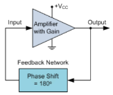
In an RC Oscillator circuit, the input is shifted 180o through the feedback circuit returning the signal out-of-phase and 180o again through an inverting amplifier stage to produces the required positive feedback.
This then gives us “180o + 180o = 360o” of phase shift which is effectively the same as 0o, thereby giving us the required positive feedback.
In other words, the total phase shift of the feedback loop should be “0” or any multiple of 360o to obtain the same effect.

The circuit on the left shows a single resistor-capacitor network whose output voltage “leads” the input voltage by some angle less than 90o.
In a pure or ideal single-pole RC network. It would produce a maximum phase shift of exactly 90o, and because 180o of phase shift is required for oscillation, at least two single-poles networks must be used within an RC oscillator design.
However, in reality it is difficult to obtain exactly 90o of phase shift for each RC stage so we must therefore use more RC stages cascaded together to obtain the required value at the oscillation frequency.
The amount of actual phase shift in the circuit depends upon the values of the resistor (R) and the capacitor (C), at the chosen frequency of oscillations with the phase angle ( φ ) being given as:
Xc = 1/2π fc R=R
Z = [ R 2 + Xc 2 ] ½
Ø = tan -1 Xc /R
Q16) Explain analog to digital converter?
A16)
Analog to digital converter samples the analog signal on each falling or rising edge of sample clock. In each cycle, the ADC gets of the analog signal, measures and converts it into a digital value. The ADC converts the output data into a series of digital values by approximates the signal with fixed precision.
In ADCs, two factors determine the accuracy of the digital value that captures the original analog signal. These are quantization level or bit rate and sampling rate.
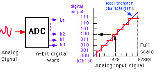
The figure depicts how analog to digital conversion takes place. Bit rate decides the resolution of digitized output
The figure displays 3-bit ADC is used for converting analog signal.

Assume that one volt signal has to be converted from digital by using 3-bit ADC as shown below. Therefore, a total of 2^3=8 divisions are available for producing 1V output. This results 1/8=0.125V is called as minimum change or quantization level represented for each division as 000 for 0V, 001 for 0.125, and likewise upto 111 for 1V. If we increase the bit rates like 6, 8, 12, 14, 16, etc. we will get a better precision of the signal. Thus, bit rate or quantization gives the smallest output change in the analog signal value that results from a change in the digital representation.
Q17) Explain hysteresis comparator?
A17)
A hysteresis comparator is operated by applying positive feedback to the comparator. The potential difference between High and Low output voltages and the feedback resistor are adjusted to change the voltage that is taken as a comparison reference to the input voltage for +IN terminal. The width of variation in the reference voltage is the hysteresis width. In this circuit the signal to -IN terminal and the output is inverted.

Q18) Explain its operation with hysteresis?
A18)
Operation with hysteresis:
Since a margin is provided between the High-to-Low and Low-to-High thresholds, no chattering occurs in the output even when a signal is input at a voltage near the threshold voltages.

When the input signal (-IN) is applied at a voltage sufficiently higher than VthH(+IN) and VthL(+IN), the output is varied according to Vref as a threshold.
When the input signal (-IN) is applied at a voltage equivalent to VthH(+IN) or above, no chattering occurs since the output will not respond unless the input falls below the threshold at VthL(+IN).
VthL is the voltage switching from Low to High.
VthH is the voltage switching from High to Low.
Q19) Explain zero crossing detector?
A19)
An op-amp detector that has the ability to detect the change from positive to negative or negative to a positive level of a sinusoidal waveform is known as a zero- crossing detector.
It is also known to be a square wave generator as the applied input signal is converted into a square wave by the zero -crossing detector.

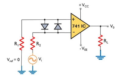
Here, the input signal Vi is provided to the inverting terminal of the op-amp while the non-inverting terminal is grounded by making use of two resistors R1 and R2.
It detects the point where the input signal crosses zero of the reference voltage level. For every crossing, the saturation level of the output signal changes from one to another.
The reference level is set at 0 and applied at the non-inverting terminal of the op-amp. The sine wave applied at the inverting terminal of the op-amp is compared with the reference level each time the phase of the wave changes either from positive to negative or negative to positive.
Firstly, when positive half of the sinusoidal signal appears at the input. Then the op-amp comparator compares the reference voltage level with the peak level of the applied signal.
Vo = Vref – Vi ---------------------------------------(1)
And we know the reference level is 0, thus
Vo = 0 – ( + Vsat) ----------------------------------------(2)
Therefore, Vo = - Vsat ---------------------------------(3)
During the negative half of the signal, thus the peak will have a negative polarity.
Again
Vo = Vref – Vi ---------------------------------------------(4)
Thus,
Vo = 0 - ( - Vsat) --------------------------------------------------(5)
So, we get
Vo = + Vsat ---------------------------------------------(6)
In this way, the zero -crossing detector detects the change in the level of the applied signal.
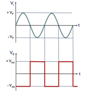
Zero crossing detector is also known to be a square wave generator. As the output of the window comparator is nothing but a square wave.

V0 for the positive half of the applied signal is – Vsat,
This is the reason why we have achieved negative half of the square wave at the output when positive half of the sinusoidal signal is applied. While V0 for the negative half of the sinusoidal signal is + Vsat,
Q20) Explain square wave generator?
A20)
Square wave generator
The square wave generator is based on a uA741 opamp (IC1). Resistor R1 and capacitor C1 determines the frequency of the square wave. Resistor R2 and R3 forms a voltage divider setup which feedbacks a fixed fraction of the output to the non-inverting input of the IC.
- Initially, when power is not applied the voltage across the capacitor C1 is 0. When the power supply is switched ON, the C1 starts charging through the resistor R1 and the output of the op-amp will be high.
- A fraction of this high voltage is fed back to the non- inverting pin by the resistor network R2, R3. When the voltage across the charging capacitor is increased to a point the voltage at the inverting pin is higher than the non-inverting pin, the output of the op-amp swings to negative saturation (-Vcc).
- The capacitor quickly discharges through R1 and starts charging in the negative direction again through R1.
- Fraction of the negative high output (-Vcc) is fed back to the non-inverting pin by the feedback network R2, R3. When the voltage across the capacitor has become so negative that the voltage at the inverting pin is less than the voltage at the non-inverting pin, the output of the op-amp swings back to the positive saturation.
- Now the capacitor discharges trough R1 and starts charging in positive direction. This cycle is repeated over time and the result is a square wave swinging between +Vcc and -Vcc at the output of the op-amp.
If the values of R2 and R3 are made equal, then the frequency of the square wave can be expressed using the following equation
F = 1/(2.1976 R1C1)
Q21) Explain triangular wave generator?
A21)
The op-amp IC used in this stage is also uA741 (IC2). Resistor R5 in conjunction with R4 sets the gain of the integrator and resistor R5 in conjunction with C2 sets the bandwidth. The square wave signal is applied to the inverting input of the op-amp through the input resistor R4. The op-amp integrator part of the circuit is shown in the figure below.

After this initial “kick” the capacitor starts charging and it creates an opposition to the input current flowing through the input resistor R4. The negative feedback compels the op-amp to produce a voltage at its out so that it maintains the virtual ground at the inverting input.
Since the capacitor is charging its impedance Xc keeps increasing and the gain Xc2/R4 also keeps increasing. This results in a ramp at the output of the op-amp that increases in a rate proportional to the RC time constant (T=R4C2) and this ramp increases in amplitude until the capacitor is fully charged.
When the input to the integrator (square wave) falls to the negative peak the capacitor quickly discharges through the input resistor R4 and starts charging in the opposite polarity.
Now the conditions are reversed, and the output of the op-amp will be a ramp that is going to the negative side at a rate proportional to the R4R2 time constant. This cycle is repeated, and the result will be a triangular waveform at the output of the op-amp integrator.
Q22) Explain precision rectifier?
A22)
A rectifier is a circuit that converts alternating current (AC) to Direct current (DC). An alternating current always changes its direction over time, but the direct current flows continuously in one direction.
In a typical rectifier circuit, we use diodes to rectify AC to DC. But this rectification method can only be used if the input voltage to the circuit is greater than the forward voltage of the diode which is typically 0.7V.
The precision rectifier is another rectifier that converts AC to DC, but in a precision rectifier we use an op-amp to compensate for the voltage drop across the diode, that is why we are not losing the 0.6V or 0.7V voltage drop across the diode, also the circuit can be constructed to have some gain at the output of the amplifier as well.
Q23) Explain half-wave precision rectifier?
A23)

Fig. Half wave precision rectifier circuit
The input and output waveform of the precision rectifier circuit, which is exactly equal to the input. That's because we are taking the feedback from the output of the diode and the op-amp compensates for any voltage drop across the diode. So, the diode behaves like an ideal diode.

Fig. When positive and negative half cycle of input signal is applied to Op-amp
Q24) Explain peak detector?
A24)
Peak detector circuits are used to determine the peak (maximum) value of an input signal. It stores the peak value of input voltages for infinite time duration until it comes to reset condition.
The peak detector circuit utilizes its property of following the highest value of an input signal and storing it.
Rectifier circuits usually provide an output in proportion to the average value of the input. However, some application requires measurement of the peak value of the signal. Thus, peak detectors are used. Usually, the peak of non-sinusoidal waveforms is measured using a peak detector.
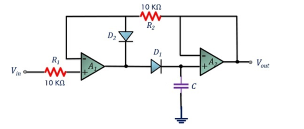
The peak of the input waveform is followed and stored in terms of voltage in the capacitor. If the circuit detects a higher peak, the new peak value is stored in the capacitor until it is discharged.
The capacitor employed in the circuit is charged through the diode by the applied input signal. The small voltage drop across the diode is ignored and the capacitor is charged up to the highest peak of the applied input signal.
Let us consider initially the capacitor is charged to voltage Vc. The diode employed in the circuit gets forward biased when the applied input voltage Vin exceeds the capacitor voltage Vc. Thereby allowing the circuit to behave as a voltage follower. The output voltage follows the applied input voltage until Vin is more than Vc.
As the input voltage Vin reduces below the value of capacitive voltage Vc, it causes the diode to get reverse biased. In such condition, the capacitor retains the value until the input again exceeds the value stored in the capacitor.
Q25) What is monoshot?
A25)
A monostable multivibrator has a “stable” state (say, Vo = 0 V) and a “transient” state (say, Vo = Vhigh). Consider the circuit to be in the stable state in the beginning.
When a certain “event” occurs, it enters the transient state, remains in that state for a time interval T, and then returns to its stable state.
Fig. (a) shows an implementation of the monostable multivibrator circuit using the Schmitt trigger of Figure.
Assume that the circuit is in the stable state in the beginning the capacitor has charged to +V ′ − (−V ′ ) = 2V ′ , the input voltage V− for the Schmitt trigger (with respect to ground) is Vo = −Vm (with Vm = VZ + Von).
And V+ = −Vm R1 R1 + R2 see Figs. (c) and (d). At t = t1, capacitor discharges and VC becomes 0 V, V− changes to −V ′, and the output Vo to +Vm.
When the capacitor starts charging since the input current of the op amp is negligibly small, the charging process can be described by
V−(t) = A e−(t−t1)/τ + B, for t > t1 , where τ = RC.
Using V−(t1) = −V ′ and V (∞) = +V ′, we get A = −2V ′ , B = V ′ ,
i.e., V−(t) = V ′ (1 − 2e −(t−t1)/τ ).
When V− crosses VT H, the output changes to +Vm (at t = t1 + T in Fig. (c).
The capacitor continues to charge, and in about five-time constants, we have once again the original stable state that we started with at t = 0.
To calculate T, we simply substitute V−(t1 + T) = VT H in Eq. and obtain
VT H = V ′ (1 − 2 e −T /τ ) → T = RC × log (2 V ′ /V ′ − VT H ).
Unit - 5
Linear & Nonlinear applications of op-amp
Q1) Explain the idealised analysis of op-amp circuits?
A1)
An Operational Amplifier is basically a three-terminal device which consists of two high impedance inputs. One of the inputs is called the Inverting Input, marked with a negative or “minus” sign, ( – ). The other input is called the Non-inverting Input, marked with a positive or “plus” sign ( + ).
A third terminal represents the operational amplifiers output port which can both sink and source either a voltage or a current.
In a linear operational amplifier, the output signal is the amplification factor, known as the amplifiers gain ( A ) multiplied by the value of the input signal and depending on the nature of these input and output signals, there can be four different classifications of operational amplifier gain.
- Voltage – Voltage “in” and Voltage “out”
- Current – Current “in” and Current “out”
- Transconductance – Voltage “in” and Current “out”
- Transresistance – Current “in” and Voltage “out”
Q2) Explain the important characteristics of op-amp?
A2)
Open Loop Gain (Avo)
The main function of an operational amplifier is to amplify the input signal and the more open loop gain it has the better. Open-loop gain is the gain of the op-amp without positive or negative feedback and for such an amplifier the gain will be infinite
Input impedance (ZIN)
Input impedance is the ratio of input voltage to input current and is assumed to be infinite to prevent any current flowing from the source supply into the amplifiers input circuitry ( IIN = 0 ). Real op-amps have input leakage currents from a few pico-amps to a few milli-amps.
Output impedance (ZOUT)
The output impedance of the ideal operational amplifier is assumed to be zero acting as a perfect internal voltage source with no internal resistance so that it can supply as much current as necessary to the load.
This internal resistance is effectively in series with the load thereby reducing the output voltage available to the load. Real op-amps have output impedances in the 100-20kΩ range.
Bandwidth (BW)
An ideal operational amplifier has an infinite frequency response and can amplify any frequency signal from DC to the highest AC frequencies, so it is therefore assumed to have an infinite bandwidth.
With real op-amps, the bandwidth is limited by the Gain-Bandwidth product (GB), which is equal to the frequency where the amplifiers gain becomes unity.
Offset Voltage (VIO)
The amplifiers output will be zero when the voltage difference between the inverting and the non-inverting inputs is zero, the same or when both inputs are grounded. Real op-amps have some amount of output offset voltage.
Q3) Explain inverting and non-inverting amplifier?
A3)
Inverting Amplifier

The input signal vi is applied to the inverting input terminal through resistor R1 and non-inverting input terminal is grounded. The feedback from the output of the inverting terminal is provided through the feedback resistor Rf.
Since the input is applied to the inverting terminal vo and vi are opposite in polarity and hence the feedback is negative. Since the non-inverting input terminal is grounded v2=0. Due to virtual short at the input of op-amp the inverting and non-inverting input terminals are at the same potential.
Therefore, v1 = v2 = 0.
Due to high input impedance of Op-amp the current flowing into its inverting input terminal is zero. Therefore, the same current flows through R1 and Rf .
i 1 = i f
But i1 = vi – v1 / R1 = vi/R1
i f = v1 – vo / Rf = -vo/Rf
Vi/R1 = - vo/Rf
Af = vo/vi = -Rf/R1
Af is the closed loop voltage gain or voltage gain with negative feedback.
Non-inverting amplifier
Non- Inverting amplifier is one in which the output is in phase with respect to input that is if you apply a positive voltage, output will be positive. The output is an non -inverted amplified version of input.

Assuming the op-amp is ideal and applying the concept of virtual short, the voltage at the inverting terminal is equal to non- inverting terminal.
Applying KCL at inverting node we get
Vi -Vo/ R2 + Vo – 0 / R1 = 0
By rearranging the terms, we will get
Voltage gain Av = Vo/ Vi = (1+ Rf/Ri)
Gain of non- inverting amplifier Av= (1+ Rf/Ri).
Q4) Explain differential amplifier?
A4)
The differential amplifier amplifies the difference between two voltages making this type of operational amplifier circuit a Subtractor This type of operational amplifier circuit is commonly known as a Differential Amplifier.
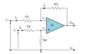
By connecting each input in turn to 0v ground we can use superposition to solve for the output voltage Vout. Then the transfer function for a Differential Amplifier circuit is given as:
I1 = V1-Va/R1 ; I2 = V2-Vb/R2 ; If = Va –(Vout)/R3
Summing Point Va =Vb
Vb = V2(R4/R2+R4)
If V2 =0 then Vout = -V1 (R3/R1)
If V1=0 then Vout = V2(R4/R2+R4)(R1+R3/R1)
Vout = -Vout (a) + Vout(b)
Vout = -V1(R3/R1) + V2(R4/R2+R4)(R1+R3/R1)
When resistors, R1 = R2 and R3 = R4 the above transfer function for the differential amplifier can be simplified to the following expression:
Vout = (V2 -V1)
The output is the difference between the two inputs hence, the op-amp can be used as subtractor.
Q5) Explain instrumentation amplifier?
A5)
The Instrumentation amplifiers consist of three op-amps. In this circuit, a non-inverting amplifier is connected to each input of the differential amplifier.
This instrumentation amplifier provides high input impedance for exact measurement of input data from transducers. The circuit diagram of an instrumentation amplifier is as shown in the figure below.
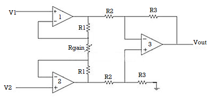
The op-amps 1 & 2 are non-inverting amplifiers and together form an input stage of the instrumentation amplifier. The op-amp 3 is a difference amplifier that forms the output stage of the instrumentation amplifier.
Working
The output stage of the instrumentation amplifier is a difference amplifier, whose output Vout is the amplified difference of the input signals applied to its input terminals.
If the outputs of op-amp 1 and op-amp 2 are Vo1 and Vo2 respectively, then the output of the difference amplifier is given by,
Vout = (R3/R2)(Vo1-Vo2)
The expressions for Vo1 and Vo2 can be found in terms of the input voltages and resistances.
Consider the input stage of the instrumentation amplifier as shown in the figure below.
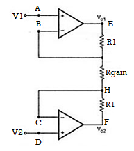
The potential at node A is the input voltage V1. Hence the potential at node B is also V1, from the virtual short concept. Thus, the potential at node G is also V1.
The potential at node D is the input voltage V2. Hence the potential at node C is also V2, from the virtual short. Thus, the potential at node H is also V2.
Ideally the current to the input stage op-amps is zero. Therefore, the current I through the resistors R1, Rgain and R1 remains the same.
Applying Ohm’s law between the nodes E and F,
I = (Vo1-Vo2)/(R1+Rgain+R1) ——————— 1
I = (Vo1-Vo2)/(2R1+Rgain)
Since no current is flowing to the input of the op-amps 1 & 2, the current I between the nodes G and H can be given as,
I = (VG-VH)/Rgain = (V1-V2)/Rgain ————————- 2
Equating equations 1 and 2,
(Vo1-Vo2)/(2R1+Rgain) = (V1-V2)/Rgain
(Vo1-Vo2) = (2R1+Rgain)(V1-V2)/Rgain —————— 3
The output of the difference amplifier is given as,
Vout = (R3/R2) (Vo1-Vo2)
Therefore, (Vo1 – Vo2) = (R2/R3)Vout
Substituting (Vo1 – Vo2) value in the equation 3, we get
(R2/R3)Vout = (2R1+Rgain)(V1-V2)/Rgain
i.e. Vout = (R3/R2){(2R1+Rgain)/Rgain}(V1-V2)
The above equation gives the output voltage of an instrumentation amplifier. The overall gain of the amplifier is given by the term (R3/R2){(2R1+Rgain)/Rgain}.
Q6) Write a short note on active filters?
A6)
Active filters are the electronic circuits, which consist of active element like op-amp(s) along with passive elements like resistor(s) and capacitor(s).
Active filters are mainly classified into the following four types based on the band of frequencies that they are allowing and / or rejecting −
- Active Low Pass Filter
- Active High Pass Filter
- Active Band Pass Filter
- Active Band Stop Filter
Q7) Explain P controller?
A7)
P Control
The Output power is directly proportional to control error. The higher the proportion coefficient, the less the output power at the same control error
Proportional control is mainly for fast-response systems with a large transmission coefficient. To adjust the proportional controller first set the maximum proportion coefficient where in the output power decreases to zero.
When the measured value is stabilized, set a specified value and gradually reduce the proportion coefficient and the control error will decrease.
If there are periodic oscillations in the system, the proportion coefficient should be increased so that control error is minimal periodic oscillations decrease to the limit.
Q8) Explain PI control?
A8)
The Output power equals to the sum of proportion and integration coefficients. The higher the proportion coefficient, the less the output power at the same control error. The higher the integration coefficient, the slower the accumulated integration coefficient.
PI control provides zero control error and and is insensitive to interference of the measurement channel. The PI control disadvantage is slow reaction to disturbances.
To adjust the PI controller first set the integration time equal to zero, and the maximum proportion time. Then by decreasing the coefficient of proportionality, achieve periodic oscillations in the system.
Q9) Explain PID control?
A9)
The Output power equals to the sum of three coefficients: proportional, integral and differential. The higher the proportion coefficient, the less the output power at the same control error.
The higher the integration coefficient, the slower the accumulated integration coefficient. The higher the differentiation coefficient, the greater the response of the system to the disturbance.
The PID controller is used in inertial systems with relatively low noise level of the measuring channel.
The advantage of PID is fast warm up time, accurate setpoint temperature control and fast reaction to disturbances.
Q10) Explain lead/lag compensator using op-amp
A10)
Lag compensator
A lag compensator is one which adds a pole to the system and is used to improve the steady state response of the system. A lag compensator provides phase lag negative phase in the frequency response of system.

Using the concept of virtual ground, the op-amp lag compensator can be redrawn as shown in the figure
Using voltage divider principle, the transfer function of the system is
Vo/Vs =(1+s*C*R1)/(1+(R1+R2)*s*C),
Hence the phase added to system is given as
Ω = tan-1(ω*C*R1) – tan-1(ω*C*(R1+R2))
Since R1<R1+R2 and tan-1(x) is increasing function (if a <b, tan-1(a)< tan1(b)) Ω is negative phase lag.
Lead compensator
A lead compensator is one which adds a zero the system and is used to improve the transient response of the system. A lead compensator provides phase lead positive phas) in the frequency response of system

Using the concept of virtual ground, the op-amp lag compensator can be redrawn as shown in the figure
Using voltage divider principle, the transfer function of the system is
Vo/Vs=(1+s*C*R1)/(1+(R1*R2/(R1+R2))*s*C),
Hence the phase added to system is given as
Ω =tan-1(ω*C*R1) -tan-1(ω*C*R1*R2/(R1+R2)).
Since R1 > R1*R2/(R1+R2) Ω is positive(phase lead).
Q11) Explain integrator using op-amp?
A11)

Since the non-inverting input terminal of op-amp is grounded v2=0. Due to virtual short at the input of op-amp the inverting and non-inverting input terminals are at the same potential
Therefore v1=v2=0
Due to high impedance of op-amp the current flowing into its input terminal is zero. Therefore the same current flows through R and C
That is
i1 = if -------------------(1)
Where i1 = vi – v1 /R = vi -/R---------------------(2)
And if = C d/dt[v1 – v0] = -C dv0/dt --------------------(3)
Substituting (2) and (3) in (1) we get
Vi = - C/R dv0/dt ------------------------(4)
Dvo/dt = (-1/RC) vi ---------------------------- (5)
Integrating both sides of eq(5) we get
v0 = - 1/RC  + v0(0) --------------------------(6)
Where v0(0) is the initial voltage on the capacitor at t=0.
Note: v0(o) represents the constant of integration.
From eq(6) we find that the output voltage is proportional to the integral of the input voltage.
Therefore v0 = - 1/RC 

Q12) The integrator circuit as shown in the figure has R = 500K Ω and C=1µF. Find and plot the output voltage for the inputs as shown in the figure.

c)vi= 2 sin 4tVd) vi= 4tV
A12)
We know that
v0 = - 1/RC  + v0(0)
Here R= 500K Ω and C = 1µF
1/RC = 1/ 500 x 1000 x 1 x 10-6
= 1/RC = 2
= -2  ; vi =- 5V
= -2 
= 10t V
Which means it is a ramp voltage with positive slope.

When vi=5V
-2  ; vi = 5V
= -2 
= -10t V
Which means it is a ramp voltage with negative slope.

When vi= 2 sin4t V
Vo = -2 
= -4 [-cos 4t] /4 cos 4t
When vi=4t V
Vo = 
= -8 [t2/2]
= - 4V

Q13) Explain the working of regulator?
A13)
By utilizing an op-amp and few other external components, linear voltage regulator is built The same circuit is also a voltage stabilizer, able to stabilize voltage at a grade better than The transistor is used to supply the load with much more current than the op-amp itself could possibly supply.
The D1 diode is a Zener -type diode and it is used for voltage reference.

Fig. Basic op-amp voltage regulator
D1 is biased through Rz. When correctly reserve biased, the Zener diode keeps the voltage across its leads close to the Zener breakdown voltage. The op-amp is used as a linear voltage amplifier.
Due to the high open loop voltage gain of the op-amp the op-amp remains in its linear region, the voltage difference between its inverting (V-) and non-inverting input (V+) is almost equal to zero.
In other words, the voltage at its non-inverting input, in respect to the ground, equals the voltage at its inverting input:
V-=V+ -------(1)
Equation (1) holds true for any op-amp working at its linear region (as an amplifier).
R1 and R2 form a voltage divider, and the voltage (V-) at their connection point is also given by the well- known voltage-divider formula:
V-=VL·R1/(R1+R2) ------ (2)
However, V+ is also equal to the Zener breakdown voltage (Vz), because the non-inverting input of the op-amp is directly connected to the cathode of the Zener diode.
V+=VZ -----------------(3)
After solving (1),(2) and (3), we get:
VL=VZ·(1+R2/R1) --------------(4)
From equation (4), we conclude that VL voltage which is the voltage applied to the load is directly proportional to the Zener voltage.
As long as Zener voltage remains stable, VL also remains stable. Additionally, the voltage applied to the load, can be easily adjusted by adjusting R1, R2 or both. For continues voltage adjustment, R1 and R2 can be replaced by a potentiometer, having its wiper at the non-inverting input of the op-amp, and its other leads at the ground and the VL line, respectively.
Q14) Explain Wein bridge oscillator?
A14)
Wien bridge oscillator is an audio frequency sine wave oscillator of high stability and simplicity. The feedback signal in this circuit is connected to the non-inverting input terminal so that the op-amp is working as a non-inverting amplifier.
The feedback network does not provide any phase shift. The circuit can be viewed as a Wien bridge with a series combination of R1 and C1 in one arm and parallel combination of R2 and C2 in the adjoining arm. Resistors R3 and R4 are connected in the remaining two arms.
The condition of zero phase shift around the circuit is achieved by balancing the bridge. The series and parallel combination of RC network form a lead-lag circuit.
At high frequencies, the reactance of capacitor C1 and C2 approaches zero. This causes C1 and C2 appears short. Here, capacitor C2 shorts the resistor R2. Hence, the output voltage Vo will be zero since output is taken across R2 and C2 combination. So, at high frequencies, circuit acts as a 'lag circuit'.
At low frequencies, both capacitors act as open because capacitor offers very high reactance. Again, output voltage will be zero because the input signal is dropped across the R1 and C1 combination. Here, the circuit acts like a 'lead circuit'.
But at one particular frequency between the two extremes, the output voltage reaches to the maximum value. At this frequency only, resistance value becomes equal to capacitive reactance and gives maximum output. Hence, this frequency is known as oscillating frequency (f).


Consider the feedback circuit, on applying voltage divider rule
Vf(s) = Vo(s) x Zp(s)/ Zp(s) + Zs(s)
Zs(s) = R1 + 1/sC1 and Zp(s) = R2|| 1/sC2
Let R1=R2=R and C1=C2=C . On solving
β = Vf(s)/ Vo(s) = RsC /(RsC) 2 + 3RsC + 1 ---------------------------(1)
Since the op-amp is operated in the non-inverting configuration the voltage gain
Av = Vo(s)/ Vf(s) = 1 + R3/R4 -------------------(2)
Applying the condition for sustained oscillations, = Av β =1
RsC /(RsC) 2 + 3RsC + 1. 1 + R3/R4
S=jw
(1 + R3/R4) ( jwRC/ - R2 C2 w2 + 3 jwRC + 1) =1
Jw RC (1 + R3/R4)= (- R2 C2 w2 + 3 jwRC + 1)
Jw[(1 + R3/R4)RC – 3RC] = 1- R2 C2 w2
To obtain the frequency of oscillation equate the real part to zero
1 - R2 C2 w2 = 0
w = 1/RC
f = 1/ 2 π RC
To obtain the condition for gain at the frequency of oscillation equate the imaginary part to zero.
Jw[(1 + R3/R4)RC – 3RC] = 0
jw[(1 + R3/R4)RC= jw3RC
[(1 + R3/R4) =3
R3/R4 =2
Therefore R3 = 2 R4 is the required condition.
Q15) Explain phase shift oscillator?
A15)
Phase Shift oscillator

In an RC Oscillator circuit, the input is shifted 180o through the feedback circuit returning the signal out-of-phase and 180o again through an inverting amplifier stage to produces the required positive feedback.
This then gives us “180o + 180o = 360o” of phase shift which is effectively the same as 0o, thereby giving us the required positive feedback.
In other words, the total phase shift of the feedback loop should be “0” or any multiple of 360o to obtain the same effect.

The circuit on the left shows a single resistor-capacitor network whose output voltage “leads” the input voltage by some angle less than 90o.
In a pure or ideal single-pole RC network. It would produce a maximum phase shift of exactly 90o, and because 180o of phase shift is required for oscillation, at least two single-poles networks must be used within an RC oscillator design.
However, in reality it is difficult to obtain exactly 90o of phase shift for each RC stage so we must therefore use more RC stages cascaded together to obtain the required value at the oscillation frequency.
The amount of actual phase shift in the circuit depends upon the values of the resistor (R) and the capacitor (C), at the chosen frequency of oscillations with the phase angle ( φ ) being given as:
Xc = 1/2π fc R=R
Z = [ R 2 + Xc 2 ] ½
Ø = tan -1 Xc /R
Q16) Explain analog to digital converter?
A16)
Analog to digital converter samples the analog signal on each falling or rising edge of sample clock. In each cycle, the ADC gets of the analog signal, measures and converts it into a digital value. The ADC converts the output data into a series of digital values by approximates the signal with fixed precision.
In ADCs, two factors determine the accuracy of the digital value that captures the original analog signal. These are quantization level or bit rate and sampling rate.
The figure depicts how analog to digital conversion takes place. Bit rate decides the resolution of digitized output
The figure displays 3-bit ADC is used for converting analog signal.
Assume that one volt signal has to be converted from digital by using 3-bit ADC as shown below. Therefore, a total of 2^3=8 divisions are available for producing 1V output. This results 1/8=0.125V is called as minimum change or quantization level represented for each division as 000 for 0V, 001 for 0.125, and likewise upto 111 for 1V. If we increase the bit rates like 6, 8, 12, 14, 16, etc. we will get a better precision of the signal. Thus, bit rate or quantization gives the smallest output change in the analog signal value that results from a change in the digital representation.
Q17) Explain hysteresis comparator?
A17)
A hysteresis comparator is operated by applying positive feedback to the comparator. The potential difference between High and Low output voltages and the feedback resistor are adjusted to change the voltage that is taken as a comparison reference to the input voltage for +IN terminal. The width of variation in the reference voltage is the hysteresis width. In this circuit the signal to -IN terminal and the output is inverted.

Q18) Explain its operation with hysteresis?
A18)
Operation with hysteresis:
Since a margin is provided between the High-to-Low and Low-to-High thresholds, no chattering occurs in the output even when a signal is input at a voltage near the threshold voltages.

When the input signal (-IN) is applied at a voltage sufficiently higher than VthH(+IN) and VthL(+IN), the output is varied according to Vref as a threshold.
When the input signal (-IN) is applied at a voltage equivalent to VthH(+IN) or above, no chattering occurs since the output will not respond unless the input falls below the threshold at VthL(+IN).
VthL is the voltage switching from Low to High.
VthH is the voltage switching from High to Low.
Q19) Explain zero crossing detector?
A19)
An op-amp detector that has the ability to detect the change from positive to negative or negative to a positive level of a sinusoidal waveform is known as a zero- crossing detector.
It is also known to be a square wave generator as the applied input signal is converted into a square wave by the zero -crossing detector.
Here, the input signal Vi is provided to the inverting terminal of the op-amp while the non-inverting terminal is grounded by making use of two resistors R1 and R2.
It detects the point where the input signal crosses zero of the reference voltage level. For every crossing, the saturation level of the output signal changes from one to another.
The reference level is set at 0 and applied at the non-inverting terminal of the op-amp. The sine wave applied at the inverting terminal of the op-amp is compared with the reference level each time the phase of the wave changes either from positive to negative or negative to positive.
Firstly, when positive half of the sinusoidal signal appears at the input. Then the op-amp comparator compares the reference voltage level with the peak level of the applied signal.
Vo = Vref – Vi ---------------------------------------(1)
And we know the reference level is 0, thus
Vo = 0 – ( + Vsat) ----------------------------------------(2)
Therefore, Vo = - Vsat ---------------------------------(3)
During the negative half of the signal, thus the peak will have a negative polarity.
Again
Vo = Vref – Vi ---------------------------------------------(4)
Thus,
Vo = 0 - ( - Vsat) --------------------------------------------------(5)
So, we get
Vo = + Vsat ---------------------------------------------(6)
In this way, the zero -crossing detector detects the change in the level of the applied signal.
Zero crossing detector is also known to be a square wave generator. As the output of the window comparator is nothing but a square wave.
V0 for the positive half of the applied signal is – Vsat,
This is the reason why we have achieved negative half of the square wave at the output when positive half of the sinusoidal signal is applied. While V0 for the negative half of the sinusoidal signal is + Vsat,
Q20) Explain square wave generator?
A20)
Square wave generator
The square wave generator is based on a uA741 opamp (IC1). Resistor R1 and capacitor C1 determines the frequency of the square wave. Resistor R2 and R3 forms a voltage divider setup which feedbacks a fixed fraction of the output to the non-inverting input of the IC.
- Initially, when power is not applied the voltage across the capacitor C1 is 0. When the power supply is switched ON, the C1 starts charging through the resistor R1 and the output of the op-amp will be high.
- A fraction of this high voltage is fed back to the non- inverting pin by the resistor network R2, R3. When the voltage across the charging capacitor is increased to a point the voltage at the inverting pin is higher than the non-inverting pin, the output of the op-amp swings to negative saturation (-Vcc).
- The capacitor quickly discharges through R1 and starts charging in the negative direction again through R1.
- Fraction of the negative high output (-Vcc) is fed back to the non-inverting pin by the feedback network R2, R3. When the voltage across the capacitor has become so negative that the voltage at the inverting pin is less than the voltage at the non-inverting pin, the output of the op-amp swings back to the positive saturation.
- Now the capacitor discharges trough R1 and starts charging in positive direction. This cycle is repeated over time and the result is a square wave swinging between +Vcc and -Vcc at the output of the op-amp.
If the values of R2 and R3 are made equal, then the frequency of the square wave can be expressed using the following equation
F = 1/(2.1976 R1C1)
Q21) Explain triangular wave generator?
A21)
The op-amp IC used in this stage is also uA741 (IC2). Resistor R5 in conjunction with R4 sets the gain of the integrator and resistor R5 in conjunction with C2 sets the bandwidth. The square wave signal is applied to the inverting input of the op-amp through the input resistor R4. The op-amp integrator part of the circuit is shown in the figure below.

After this initial “kick” the capacitor starts charging and it creates an opposition to the input current flowing through the input resistor R4. The negative feedback compels the op-amp to produce a voltage at its out so that it maintains the virtual ground at the inverting input.
Since the capacitor is charging its impedance Xc keeps increasing and the gain Xc2/R4 also keeps increasing. This results in a ramp at the output of the op-amp that increases in a rate proportional to the RC time constant (T=R4C2) and this ramp increases in amplitude until the capacitor is fully charged.
When the input to the integrator (square wave) falls to the negative peak the capacitor quickly discharges through the input resistor R4 and starts charging in the opposite polarity.
Now the conditions are reversed, and the output of the op-amp will be a ramp that is going to the negative side at a rate proportional to the R4R2 time constant. This cycle is repeated, and the result will be a triangular waveform at the output of the op-amp integrator.
Q22) Explain precision rectifier?
A22)
A rectifier is a circuit that converts alternating current (AC) to Direct current (DC). An alternating current always changes its direction over time, but the direct current flows continuously in one direction.
In a typical rectifier circuit, we use diodes to rectify AC to DC. But this rectification method can only be used if the input voltage to the circuit is greater than the forward voltage of the diode which is typically 0.7V.
The precision rectifier is another rectifier that converts AC to DC, but in a precision rectifier we use an op-amp to compensate for the voltage drop across the diode, that is why we are not losing the 0.6V or 0.7V voltage drop across the diode, also the circuit can be constructed to have some gain at the output of the amplifier as well.
Q23) Explain half-wave precision rectifier?
A23)

Fig. Half wave precision rectifier circuit
The input and output waveform of the precision rectifier circuit, which is exactly equal to the input. That's because we are taking the feedback from the output of the diode and the op-amp compensates for any voltage drop across the diode. So, the diode behaves like an ideal diode.

Fig. When positive and negative half cycle of input signal is applied to Op-amp
Q24) Explain peak detector?
A24)
Peak detector circuits are used to determine the peak (maximum) value of an input signal. It stores the peak value of input voltages for infinite time duration until it comes to reset condition.
The peak detector circuit utilizes its property of following the highest value of an input signal and storing it.
Rectifier circuits usually provide an output in proportion to the average value of the input. However, some application requires measurement of the peak value of the signal. Thus, peak detectors are used. Usually, the peak of non-sinusoidal waveforms is measured using a peak detector.

The peak of the input waveform is followed and stored in terms of voltage in the capacitor. If the circuit detects a higher peak, the new peak value is stored in the capacitor until it is discharged.
The capacitor employed in the circuit is charged through the diode by the applied input signal. The small voltage drop across the diode is ignored and the capacitor is charged up to the highest peak of the applied input signal.
Let us consider initially the capacitor is charged to voltage Vc. The diode employed in the circuit gets forward biased when the applied input voltage Vin exceeds the capacitor voltage Vc. Thereby allowing the circuit to behave as a voltage follower. The output voltage follows the applied input voltage until Vin is more than Vc.
As the input voltage Vin reduces below the value of capacitive voltage Vc, it causes the diode to get reverse biased. In such condition, the capacitor retains the value until the input again exceeds the value stored in the capacitor.
Q25) What is monoshot?
A25)
A monostable multivibrator has a “stable” state (say, Vo = 0 V) and a “transient” state (say, Vo = Vhigh). Consider the circuit to be in the stable state in the beginning.
When a certain “event” occurs, it enters the transient state, remains in that state for a time interval T, and then returns to its stable state.
Fig. (a) shows an implementation of the monostable multivibrator circuit using the Schmitt trigger of Figure.
Assume that the circuit is in the stable state in the beginning the capacitor has charged to +V ′ − (−V ′ ) = 2V ′ , the input voltage V− for the Schmitt trigger (with respect to ground) is Vo = −Vm (with Vm = VZ + Von).
And V+ = −Vm R1 R1 + R2 see Figs. (c) and (d). At t = t1, capacitor discharges and VC becomes 0 V, V− changes to −V ′, and the output Vo to +Vm.
When the capacitor starts charging since the input current of the op amp is negligibly small, the charging process can be described by
V−(t) = A e−(t−t1)/τ + B, for t > t1 , where τ = RC.
Using V−(t1) = −V ′ and V (∞) = +V ′, we get A = −2V ′ , B = V ′ ,
i.e., V−(t) = V ′ (1 − 2e −(t−t1)/τ ).
When V− crosses VT H, the output changes to +Vm (at t = t1 + T in Fig. (c).
The capacitor continues to charge, and in about five-time constants, we have once again the original stable state that we started with at t = 0.
To calculate T, we simply substitute V−(t1 + T) = VT H in Eq. and obtain
VT H = V ′ (1 − 2 e −T /τ ) → T = RC × log (2 V ′ /V ′ − VT H ).
Unit - 5
Linear & Nonlinear applications of op-amp
Q1) Explain the idealised analysis of op-amp circuits?
A1)
An Operational Amplifier is basically a three-terminal device which consists of two high impedance inputs. One of the inputs is called the Inverting Input, marked with a negative or “minus” sign, ( – ). The other input is called the Non-inverting Input, marked with a positive or “plus” sign ( + ).
A third terminal represents the operational amplifiers output port which can both sink and source either a voltage or a current.
In a linear operational amplifier, the output signal is the amplification factor, known as the amplifiers gain ( A ) multiplied by the value of the input signal and depending on the nature of these input and output signals, there can be four different classifications of operational amplifier gain.
- Voltage – Voltage “in” and Voltage “out”
- Current – Current “in” and Current “out”
- Transconductance – Voltage “in” and Current “out”
- Transresistance – Current “in” and Voltage “out”
Q2) Explain the important characteristics of op-amp?
A2)
Open Loop Gain (Avo)
The main function of an operational amplifier is to amplify the input signal and the more open loop gain it has the better. Open-loop gain is the gain of the op-amp without positive or negative feedback and for such an amplifier the gain will be infinite
Input impedance (ZIN)
Input impedance is the ratio of input voltage to input current and is assumed to be infinite to prevent any current flowing from the source supply into the amplifiers input circuitry ( IIN = 0 ). Real op-amps have input leakage currents from a few pico-amps to a few milli-amps.
Output impedance (ZOUT)
The output impedance of the ideal operational amplifier is assumed to be zero acting as a perfect internal voltage source with no internal resistance so that it can supply as much current as necessary to the load.
This internal resistance is effectively in series with the load thereby reducing the output voltage available to the load. Real op-amps have output impedances in the 100-20kΩ range.
Bandwidth (BW)
An ideal operational amplifier has an infinite frequency response and can amplify any frequency signal from DC to the highest AC frequencies, so it is therefore assumed to have an infinite bandwidth.
With real op-amps, the bandwidth is limited by the Gain-Bandwidth product (GB), which is equal to the frequency where the amplifiers gain becomes unity.
Offset Voltage (VIO)
The amplifiers output will be zero when the voltage difference between the inverting and the non-inverting inputs is zero, the same or when both inputs are grounded. Real op-amps have some amount of output offset voltage.
Q3) Explain inverting and non-inverting amplifier?
A3)
Inverting Amplifier

The input signal vi is applied to the inverting input terminal through resistor R1 and non-inverting input terminal is grounded. The feedback from the output of the inverting terminal is provided through the feedback resistor Rf.
Since the input is applied to the inverting terminal vo and vi are opposite in polarity and hence the feedback is negative. Since the non-inverting input terminal is grounded v2=0. Due to virtual short at the input of op-amp the inverting and non-inverting input terminals are at the same potential.
Therefore, v1 = v2 = 0.
Due to high input impedance of Op-amp the current flowing into its inverting input terminal is zero. Therefore, the same current flows through R1 and Rf .
i 1 = i f
But i1 = vi – v1 / R1 = vi/R1
i f = v1 – vo / Rf = -vo/Rf
Vi/R1 = - vo/Rf
Af = vo/vi = -Rf/R1
Af is the closed loop voltage gain or voltage gain with negative feedback.
Non-inverting amplifier
Non- Inverting amplifier is one in which the output is in phase with respect to input that is if you apply a positive voltage, output will be positive. The output is an non -inverted amplified version of input.

Assuming the op-amp is ideal and applying the concept of virtual short, the voltage at the inverting terminal is equal to non- inverting terminal.
Applying KCL at inverting node we get
Vi -Vo/ R2 + Vo – 0 / R1 = 0
By rearranging the terms, we will get
Voltage gain Av = Vo/ Vi = (1+ Rf/Ri)
Gain of non- inverting amplifier Av= (1+ Rf/Ri).
Q4) Explain differential amplifier?
A4)
The differential amplifier amplifies the difference between two voltages making this type of operational amplifier circuit a Subtractor This type of operational amplifier circuit is commonly known as a Differential Amplifier.

By connecting each input in turn to 0v ground we can use superposition to solve for the output voltage Vout. Then the transfer function for a Differential Amplifier circuit is given as:
I1 = V1-Va/R1 ; I2 = V2-Vb/R2 ; If = Va –(Vout)/R3
Summing Point Va =Vb
Vb = V2(R4/R2+R4)
If V2 =0 then Vout = -V1 (R3/R1)
If V1=0 then Vout = V2(R4/R2+R4)(R1+R3/R1)
Vout = -Vout (a) + Vout(b)
Vout = -V1(R3/R1) + V2(R4/R2+R4)(R1+R3/R1)
When resistors, R1 = R2 and R3 = R4 the above transfer function for the differential amplifier can be simplified to the following expression:
Vout = (V2 -V1)
The output is the difference between the two inputs hence, the op-amp can be used as subtractor.
Q5) Explain instrumentation amplifier?
A5)
The Instrumentation amplifiers consist of three op-amps. In this circuit, a non-inverting amplifier is connected to each input of the differential amplifier.
This instrumentation amplifier provides high input impedance for exact measurement of input data from transducers. The circuit diagram of an instrumentation amplifier is as shown in the figure below.

The op-amps 1 & 2 are non-inverting amplifiers and together form an input stage of the instrumentation amplifier. The op-amp 3 is a difference amplifier that forms the output stage of the instrumentation amplifier.
Working
The output stage of the instrumentation amplifier is a difference amplifier, whose output Vout is the amplified difference of the input signals applied to its input terminals.
If the outputs of op-amp 1 and op-amp 2 are Vo1 and Vo2 respectively, then the output of the difference amplifier is given by,
Vout = (R3/R2)(Vo1-Vo2)
The expressions for Vo1 and Vo2 can be found in terms of the input voltages and resistances.
Consider the input stage of the instrumentation amplifier as shown in the figure below.

The potential at node A is the input voltage V1. Hence the potential at node B is also V1, from the virtual short concept. Thus, the potential at node G is also V1.
The potential at node D is the input voltage V2. Hence the potential at node C is also V2, from the virtual short. Thus, the potential at node H is also V2.
Ideally the current to the input stage op-amps is zero. Therefore, the current I through the resistors R1, Rgain and R1 remains the same.
Applying Ohm’s law between the nodes E and F,
I = (Vo1-Vo2)/(R1+Rgain+R1) ——————— 1
I = (Vo1-Vo2)/(2R1+Rgain)
Since no current is flowing to the input of the op-amps 1 & 2, the current I between the nodes G and H can be given as,
I = (VG-VH)/Rgain = (V1-V2)/Rgain ————————- 2
Equating equations 1 and 2,
(Vo1-Vo2)/(2R1+Rgain) = (V1-V2)/Rgain
(Vo1-Vo2) = (2R1+Rgain)(V1-V2)/Rgain —————— 3
The output of the difference amplifier is given as,
Vout = (R3/R2) (Vo1-Vo2)
Therefore, (Vo1 – Vo2) = (R2/R3)Vout
Substituting (Vo1 – Vo2) value in the equation 3, we get
(R2/R3)Vout = (2R1+Rgain)(V1-V2)/Rgain
i.e. Vout = (R3/R2){(2R1+Rgain)/Rgain}(V1-V2)
The above equation gives the output voltage of an instrumentation amplifier. The overall gain of the amplifier is given by the term (R3/R2){(2R1+Rgain)/Rgain}.
Q6) Write a short note on active filters?
A6)
Active filters are the electronic circuits, which consist of active element like op-amp(s) along with passive elements like resistor(s) and capacitor(s).
Active filters are mainly classified into the following four types based on the band of frequencies that they are allowing and / or rejecting −
- Active Low Pass Filter
- Active High Pass Filter
- Active Band Pass Filter
- Active Band Stop Filter
Q7) Explain P controller?
A7)
P Control
The Output power is directly proportional to control error. The higher the proportion coefficient, the less the output power at the same control error
Proportional control is mainly for fast-response systems with a large transmission coefficient. To adjust the proportional controller first set the maximum proportion coefficient where in the output power decreases to zero.
When the measured value is stabilized, set a specified value and gradually reduce the proportion coefficient and the control error will decrease.
If there are periodic oscillations in the system, the proportion coefficient should be increased so that control error is minimal periodic oscillations decrease to the limit.
Q8) Explain PI control?
A8)
The Output power equals to the sum of proportion and integration coefficients. The higher the proportion coefficient, the less the output power at the same control error. The higher the integration coefficient, the slower the accumulated integration coefficient.
PI control provides zero control error and and is insensitive to interference of the measurement channel. The PI control disadvantage is slow reaction to disturbances.
To adjust the PI controller first set the integration time equal to zero, and the maximum proportion time. Then by decreasing the coefficient of proportionality, achieve periodic oscillations in the system.
Q9) Explain PID control?
A9)
The Output power equals to the sum of three coefficients: proportional, integral and differential. The higher the proportion coefficient, the less the output power at the same control error.
The higher the integration coefficient, the slower the accumulated integration coefficient. The higher the differentiation coefficient, the greater the response of the system to the disturbance.
The PID controller is used in inertial systems with relatively low noise level of the measuring channel.
The advantage of PID is fast warm up time, accurate setpoint temperature control and fast reaction to disturbances.
Q10) Explain lead/lag compensator using op-amp
A10)
Lag compensator
A lag compensator is one which adds a pole to the system and is used to improve the steady state response of the system. A lag compensator provides phase lag negative phase in the frequency response of system.

Using the concept of virtual ground, the op-amp lag compensator can be redrawn as shown in the figure
Using voltage divider principle, the transfer function of the system is
Vo/Vs =(1+s*C*R1)/(1+(R1+R2)*s*C),
Hence the phase added to system is given as
Ω = tan-1(ω*C*R1) – tan-1(ω*C*(R1+R2))
Since R1<R1+R2 and tan-1(x) is increasing function (if a <b, tan-1(a)< tan1(b)) Ω is negative phase lag.
Lead compensator
A lead compensator is one which adds a zero the system and is used to improve the transient response of the system. A lead compensator provides phase lead positive phas) in the frequency response of system

Using the concept of virtual ground, the op-amp lag compensator can be redrawn as shown in the figure
Using voltage divider principle, the transfer function of the system is
Vo/Vs=(1+s*C*R1)/(1+(R1*R2/(R1+R2))*s*C),
Hence the phase added to system is given as
Ω =tan-1(ω*C*R1) -tan-1(ω*C*R1*R2/(R1+R2)).
Since R1 > R1*R2/(R1+R2) Ω is positive(phase lead).
Q11) Explain integrator using op-amp?
A11)

Since the non-inverting input terminal of op-amp is grounded v2=0. Due to virtual short at the input of op-amp the inverting and non-inverting input terminals are at the same potential
Therefore v1=v2=0
Due to high impedance of op-amp the current flowing into its input terminal is zero. Therefore the same current flows through R and C
That is
i1 = if -------------------(1)
Where i1 = vi – v1 /R = vi -/R---------------------(2)
And if = C d/dt[v1 – v0] = -C dv0/dt --------------------(3)
Substituting (2) and (3) in (1) we get
Vi = - C/R dv0/dt ------------------------(4)
Dvo/dt = (-1/RC) vi ---------------------------- (5)
Integrating both sides of eq(5) we get
v0 = - 1/RC  + v0(0) --------------------------(6)
Where v0(0) is the initial voltage on the capacitor at t=0.
Note: v0(o) represents the constant of integration.
From eq(6) we find that the output voltage is proportional to the integral of the input voltage.
Therefore v0 = - 1/RC 

Q12) The integrator circuit as shown in the figure has R = 500K Ω and C=1µF. Find and plot the output voltage for the inputs as shown in the figure.

c)vi= 2 sin 4tVd) vi= 4tV
A12)
We know that
v0 = - 1/RC  + v0(0)
Here R= 500K Ω and C = 1µF
1/RC = 1/ 500 x 1000 x 1 x 10-6
= 1/RC = 2
= -2  ; vi =- 5V
= -2 
= 10t V
Which means it is a ramp voltage with positive slope.

When vi=5V
-2  ; vi = 5V
= -2 
= -10t V
Which means it is a ramp voltage with negative slope.

When vi= 2 sin4t V
Vo = -2 
= -4 [-cos 4t] /4 cos 4t

When vi=4t V
Vo = 
= -8 [t2/2]
= - 4V

Q13) Explain the working of regulator?
A13)
By utilizing an op-amp and few other external components, linear voltage regulator is built The same circuit is also a voltage stabilizer, able to stabilize voltage at a grade better than The transistor is used to supply the load with much more current than the op-amp itself could possibly supply.
The D1 diode is a Zener -type diode and it is used for voltage reference.

Fig. Basic op-amp voltage regulator
D1 is biased through Rz. When correctly reserve biased, the Zener diode keeps the voltage across its leads close to the Zener breakdown voltage. The op-amp is used as a linear voltage amplifier.
Due to the high open loop voltage gain of the op-amp the op-amp remains in its linear region, the voltage difference between its inverting (V-) and non-inverting input (V+) is almost equal to zero.
In other words, the voltage at its non-inverting input, in respect to the ground, equals the voltage at its inverting input:
V-=V+ -------(1)
Equation (1) holds true for any op-amp working at its linear region (as an amplifier).
R1 and R2 form a voltage divider, and the voltage (V-) at their connection point is also given by the well- known voltage-divider formula:
V-=VL·R1/(R1+R2) ------ (2)
However, V+ is also equal to the Zener breakdown voltage (Vz), because the non-inverting input of the op-amp is directly connected to the cathode of the Zener diode.
V+=VZ -----------------(3)
After solving (1),(2) and (3), we get:
VL=VZ·(1+R2/R1) --------------(4)
From equation (4), we conclude that VL voltage which is the voltage applied to the load is directly proportional to the Zener voltage.
As long as Zener voltage remains stable, VL also remains stable. Additionally, the voltage applied to the load, can be easily adjusted by adjusting R1, R2 or both. For continues voltage adjustment, R1 and R2 can be replaced by a potentiometer, having its wiper at the non-inverting input of the op-amp, and its other leads at the ground and the VL line, respectively.
Q14) Explain Wein bridge oscillator?
A14)
Wien bridge oscillator is an audio frequency sine wave oscillator of high stability and simplicity. The feedback signal in this circuit is connected to the non-inverting input terminal so that the op-amp is working as a non-inverting amplifier.
The feedback network does not provide any phase shift. The circuit can be viewed as a Wien bridge with a series combination of R1 and C1 in one arm and parallel combination of R2 and C2 in the adjoining arm. Resistors R3 and R4 are connected in the remaining two arms.
The condition of zero phase shift around the circuit is achieved by balancing the bridge. The series and parallel combination of RC network form a lead-lag circuit.
At high frequencies, the reactance of capacitor C1 and C2 approaches zero. This causes C1 and C2 appears short. Here, capacitor C2 shorts the resistor R2. Hence, the output voltage Vo will be zero since output is taken across R2 and C2 combination. So, at high frequencies, circuit acts as a 'lag circuit'.
At low frequencies, both capacitors act as open because capacitor offers very high reactance. Again, output voltage will be zero because the input signal is dropped across the R1 and C1 combination. Here, the circuit acts like a 'lead circuit'.
But at one particular frequency between the two extremes, the output voltage reaches to the maximum value. At this frequency only, resistance value becomes equal to capacitive reactance and gives maximum output. Hence, this frequency is known as oscillating frequency (f).

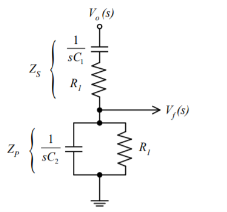
Consider the feedback circuit, on applying voltage divider rule
Vf(s) = Vo(s) x Zp(s)/ Zp(s) + Zs(s)
Zs(s) = R1 + 1/sC1 and Zp(s) = R2|| 1/sC2
Let R1=R2=R and C1=C2=C . On solving
β = Vf(s)/ Vo(s) = RsC /(RsC) 2 + 3RsC + 1 ---------------------------(1)
Since the op-amp is operated in the non-inverting configuration the voltage gain
Av = Vo(s)/ Vf(s) = 1 + R3/R4 -------------------(2)
Applying the condition for sustained oscillations, = Av β =1
RsC /(RsC) 2 + 3RsC + 1. 1 + R3/R4
S=jw
(1 + R3/R4) ( jwRC/ - R2 C2 w2 + 3 jwRC + 1) =1
Jw RC (1 + R3/R4)= (- R2 C2 w2 + 3 jwRC + 1)
Jw[(1 + R3/R4)RC – 3RC] = 1- R2 C2 w2
To obtain the frequency of oscillation equate the real part to zero
1 - R2 C2 w2 = 0
w = 1/RC
f = 1/ 2 π RC
To obtain the condition for gain at the frequency of oscillation equate the imaginary part to zero.
Jw[(1 + R3/R4)RC – 3RC] = 0
jw[(1 + R3/R4)RC= jw3RC
[(1 + R3/R4) =3
R3/R4 =2
Therefore R3 = 2 R4 is the required condition.
Q15) Explain phase shift oscillator?
A15)
Phase Shift oscillator

In an RC Oscillator circuit, the input is shifted 180o through the feedback circuit returning the signal out-of-phase and 180o again through an inverting amplifier stage to produces the required positive feedback.
This then gives us “180o + 180o = 360o” of phase shift which is effectively the same as 0o, thereby giving us the required positive feedback.
In other words, the total phase shift of the feedback loop should be “0” or any multiple of 360o to obtain the same effect.
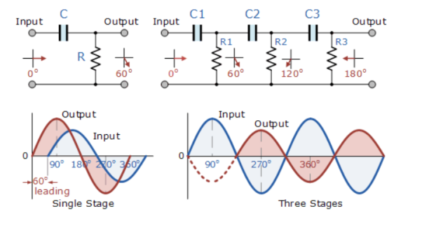
The circuit on the left shows a single resistor-capacitor network whose output voltage “leads” the input voltage by some angle less than 90o.
In a pure or ideal single-pole RC network. It would produce a maximum phase shift of exactly 90o, and because 180o of phase shift is required for oscillation, at least two single-poles networks must be used within an RC oscillator design.
However, in reality it is difficult to obtain exactly 90o of phase shift for each RC stage so we must therefore use more RC stages cascaded together to obtain the required value at the oscillation frequency.
The amount of actual phase shift in the circuit depends upon the values of the resistor (R) and the capacitor (C), at the chosen frequency of oscillations with the phase angle ( φ ) being given as:
Xc = 1/2π fc R=R
Z = [ R 2 + Xc 2 ] ½
Ø = tan -1 Xc /R
Q16) Explain analog to digital converter?
A16)
Analog to digital converter samples the analog signal on each falling or rising edge of sample clock. In each cycle, the ADC gets of the analog signal, measures and converts it into a digital value. The ADC converts the output data into a series of digital values by approximates the signal with fixed precision.
In ADCs, two factors determine the accuracy of the digital value that captures the original analog signal. These are quantization level or bit rate and sampling rate.
The figure depicts how analog to digital conversion takes place. Bit rate decides the resolution of digitized output
The figure displays 3-bit ADC is used for converting analog signal.

Assume that one volt signal has to be converted from digital by using 3-bit ADC as shown below. Therefore, a total of 2^3=8 divisions are available for producing 1V output. This results 1/8=0.125V is called as minimum change or quantization level represented for each division as 000 for 0V, 001 for 0.125, and likewise upto 111 for 1V. If we increase the bit rates like 6, 8, 12, 14, 16, etc. we will get a better precision of the signal. Thus, bit rate or quantization gives the smallest output change in the analog signal value that results from a change in the digital representation.
Q17) Explain hysteresis comparator?
A17)
A hysteresis comparator is operated by applying positive feedback to the comparator. The potential difference between High and Low output voltages and the feedback resistor are adjusted to change the voltage that is taken as a comparison reference to the input voltage for +IN terminal. The width of variation in the reference voltage is the hysteresis width. In this circuit the signal to -IN terminal and the output is inverted.

Q18) Explain its operation with hysteresis?
A18)
Operation with hysteresis:
Since a margin is provided between the High-to-Low and Low-to-High thresholds, no chattering occurs in the output even when a signal is input at a voltage near the threshold voltages.

When the input signal (-IN) is applied at a voltage sufficiently higher than VthH(+IN) and VthL(+IN), the output is varied according to Vref as a threshold.
When the input signal (-IN) is applied at a voltage equivalent to VthH(+IN) or above, no chattering occurs since the output will not respond unless the input falls below the threshold at VthL(+IN).
VthL is the voltage switching from Low to High.
VthH is the voltage switching from High to Low.
Q19) Explain zero crossing detector?
A19)
An op-amp detector that has the ability to detect the change from positive to negative or negative to a positive level of a sinusoidal waveform is known as a zero- crossing detector.
It is also known to be a square wave generator as the applied input signal is converted into a square wave by the zero -crossing detector.

Here, the input signal Vi is provided to the inverting terminal of the op-amp while the non-inverting terminal is grounded by making use of two resistors R1 and R2.
It detects the point where the input signal crosses zero of the reference voltage level. For every crossing, the saturation level of the output signal changes from one to another.
The reference level is set at 0 and applied at the non-inverting terminal of the op-amp. The sine wave applied at the inverting terminal of the op-amp is compared with the reference level each time the phase of the wave changes either from positive to negative or negative to positive.
Firstly, when positive half of the sinusoidal signal appears at the input. Then the op-amp comparator compares the reference voltage level with the peak level of the applied signal.
Vo = Vref – Vi ---------------------------------------(1)
And we know the reference level is 0, thus
Vo = 0 – ( + Vsat) ----------------------------------------(2)
Therefore, Vo = - Vsat ---------------------------------(3)
During the negative half of the signal, thus the peak will have a negative polarity.
Again
Vo = Vref – Vi ---------------------------------------------(4)
Thus,
Vo = 0 - ( - Vsat) --------------------------------------------------(5)
So, we get
Vo = + Vsat ---------------------------------------------(6)
In this way, the zero -crossing detector detects the change in the level of the applied signal.
Zero crossing detector is also known to be a square wave generator. As the output of the window comparator is nothing but a square wave.

V0 for the positive half of the applied signal is – Vsat,
This is the reason why we have achieved negative half of the square wave at the output when positive half of the sinusoidal signal is applied. While V0 for the negative half of the sinusoidal signal is + Vsat,
Q20) Explain square wave generator?
A20)
Square wave generator
The square wave generator is based on a uA741 opamp (IC1). Resistor R1 and capacitor C1 determines the frequency of the square wave. Resistor R2 and R3 forms a voltage divider setup which feedbacks a fixed fraction of the output to the non-inverting input of the IC.
- Initially, when power is not applied the voltage across the capacitor C1 is 0. When the power supply is switched ON, the C1 starts charging through the resistor R1 and the output of the op-amp will be high.
- A fraction of this high voltage is fed back to the non- inverting pin by the resistor network R2, R3. When the voltage across the charging capacitor is increased to a point the voltage at the inverting pin is higher than the non-inverting pin, the output of the op-amp swings to negative saturation (-Vcc).
- The capacitor quickly discharges through R1 and starts charging in the negative direction again through R1.
- Fraction of the negative high output (-Vcc) is fed back to the non-inverting pin by the feedback network R2, R3. When the voltage across the capacitor has become so negative that the voltage at the inverting pin is less than the voltage at the non-inverting pin, the output of the op-amp swings back to the positive saturation.
- Now the capacitor discharges trough R1 and starts charging in positive direction. This cycle is repeated over time and the result is a square wave swinging between +Vcc and -Vcc at the output of the op-amp.
If the values of R2 and R3 are made equal, then the frequency of the square wave can be expressed using the following equation
F = 1/(2.1976 R1C1)
Q21) Explain triangular wave generator?
A21)
The op-amp IC used in this stage is also uA741 (IC2). Resistor R5 in conjunction with R4 sets the gain of the integrator and resistor R5 in conjunction with C2 sets the bandwidth. The square wave signal is applied to the inverting input of the op-amp through the input resistor R4. The op-amp integrator part of the circuit is shown in the figure below.
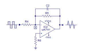
After this initial “kick” the capacitor starts charging and it creates an opposition to the input current flowing through the input resistor R4. The negative feedback compels the op-amp to produce a voltage at its out so that it maintains the virtual ground at the inverting input.
Since the capacitor is charging its impedance Xc keeps increasing and the gain Xc2/R4 also keeps increasing. This results in a ramp at the output of the op-amp that increases in a rate proportional to the RC time constant (T=R4C2) and this ramp increases in amplitude until the capacitor is fully charged.
When the input to the integrator (square wave) falls to the negative peak the capacitor quickly discharges through the input resistor R4 and starts charging in the opposite polarity.
Now the conditions are reversed, and the output of the op-amp will be a ramp that is going to the negative side at a rate proportional to the R4R2 time constant. This cycle is repeated, and the result will be a triangular waveform at the output of the op-amp integrator.
Q22) Explain precision rectifier?
A22)
A rectifier is a circuit that converts alternating current (AC) to Direct current (DC). An alternating current always changes its direction over time, but the direct current flows continuously in one direction.
In a typical rectifier circuit, we use diodes to rectify AC to DC. But this rectification method can only be used if the input voltage to the circuit is greater than the forward voltage of the diode which is typically 0.7V.
The precision rectifier is another rectifier that converts AC to DC, but in a precision rectifier we use an op-amp to compensate for the voltage drop across the diode, that is why we are not losing the 0.6V or 0.7V voltage drop across the diode, also the circuit can be constructed to have some gain at the output of the amplifier as well.
Q23) Explain half-wave precision rectifier?
A23)
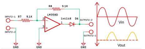
Fig. Half wave precision rectifier circuit
The input and output waveform of the precision rectifier circuit, which is exactly equal to the input. That's because we are taking the feedback from the output of the diode and the op-amp compensates for any voltage drop across the diode. So, the diode behaves like an ideal diode.

Fig. When positive and negative half cycle of input signal is applied to Op-amp
Q24) Explain peak detector?
A24)
Peak detector circuits are used to determine the peak (maximum) value of an input signal. It stores the peak value of input voltages for infinite time duration until it comes to reset condition.
The peak detector circuit utilizes its property of following the highest value of an input signal and storing it.
Rectifier circuits usually provide an output in proportion to the average value of the input. However, some application requires measurement of the peak value of the signal. Thus, peak detectors are used. Usually, the peak of non-sinusoidal waveforms is measured using a peak detector.

The peak of the input waveform is followed and stored in terms of voltage in the capacitor. If the circuit detects a higher peak, the new peak value is stored in the capacitor until it is discharged.
The capacitor employed in the circuit is charged through the diode by the applied input signal. The small voltage drop across the diode is ignored and the capacitor is charged up to the highest peak of the applied input signal.
Let us consider initially the capacitor is charged to voltage Vc. The diode employed in the circuit gets forward biased when the applied input voltage Vin exceeds the capacitor voltage Vc. Thereby allowing the circuit to behave as a voltage follower. The output voltage follows the applied input voltage until Vin is more than Vc.
As the input voltage Vin reduces below the value of capacitive voltage Vc, it causes the diode to get reverse biased. In such condition, the capacitor retains the value until the input again exceeds the value stored in the capacitor.
Q25) What is monoshot?
A25)
A monostable multivibrator has a “stable” state (say, Vo = 0 V) and a “transient” state (say, Vo = Vhigh). Consider the circuit to be in the stable state in the beginning.
When a certain “event” occurs, it enters the transient state, remains in that state for a time interval T, and then returns to its stable state.
Fig. (a) shows an implementation of the monostable multivibrator circuit using the Schmitt trigger of Figure.
Assume that the circuit is in the stable state in the beginning the capacitor has charged to +V ′ − (−V ′ ) = 2V ′ , the input voltage V− for the Schmitt trigger (with respect to ground) is Vo = −Vm (with Vm = VZ + Von).
And V+ = −Vm R1 R1 + R2 see Figs. (c) and (d). At t = t1, capacitor discharges and VC becomes 0 V, V− changes to −V ′, and the output Vo to +Vm.
When the capacitor starts charging since the input current of the op amp is negligibly small, the charging process can be described by
V−(t) = A e−(t−t1)/τ + B, for t > t1 , where τ = RC.
Using V−(t1) = −V ′ and V (∞) = +V ′, we get A = −2V ′ , B = V ′ ,
i.e., V−(t) = V ′ (1 − 2e −(t−t1)/τ ).
When V− crosses VT H, the output changes to +Vm (at t = t1 + T in Fig. (c).
The capacitor continues to charge, and in about five-time constants, we have once again the original stable state that we started with at t = 0.
To calculate T, we simply substitute V−(t1 + T) = VT H in Eq. and obtain
VT H = V ′ (1 − 2 e −T /τ ) → T = RC × log (2 V ′ /V ′ − VT H ).
Unit - 5
Unit - 5
Linear & Nonlinear applications of op-amp
Q1) Explain the idealised analysis of op-amp circuits?
A1)
An Operational Amplifier is basically a three-terminal device which consists of two high impedance inputs. One of the inputs is called the Inverting Input, marked with a negative or “minus” sign, ( – ). The other input is called the Non-inverting Input, marked with a positive or “plus” sign ( + ).
A third terminal represents the operational amplifiers output port which can both sink and source either a voltage or a current.
In a linear operational amplifier, the output signal is the amplification factor, known as the amplifiers gain ( A ) multiplied by the value of the input signal and depending on the nature of these input and output signals, there can be four different classifications of operational amplifier gain.
- Voltage – Voltage “in” and Voltage “out”
- Current – Current “in” and Current “out”
- Transconductance – Voltage “in” and Current “out”
- Transresistance – Current “in” and Voltage “out”
Q2) Explain the important characteristics of op-amp?
A2)
Open Loop Gain (Avo)
The main function of an operational amplifier is to amplify the input signal and the more open loop gain it has the better. Open-loop gain is the gain of the op-amp without positive or negative feedback and for such an amplifier the gain will be infinite
Input impedance (ZIN)
Input impedance is the ratio of input voltage to input current and is assumed to be infinite to prevent any current flowing from the source supply into the amplifiers input circuitry ( IIN = 0 ). Real op-amps have input leakage currents from a few pico-amps to a few milli-amps.
Output impedance (ZOUT)
The output impedance of the ideal operational amplifier is assumed to be zero acting as a perfect internal voltage source with no internal resistance so that it can supply as much current as necessary to the load.
This internal resistance is effectively in series with the load thereby reducing the output voltage available to the load. Real op-amps have output impedances in the 100-20kΩ range.
Bandwidth (BW)
An ideal operational amplifier has an infinite frequency response and can amplify any frequency signal from DC to the highest AC frequencies, so it is therefore assumed to have an infinite bandwidth.
With real op-amps, the bandwidth is limited by the Gain-Bandwidth product (GB), which is equal to the frequency where the amplifiers gain becomes unity.
Offset Voltage (VIO)
The amplifiers output will be zero when the voltage difference between the inverting and the non-inverting inputs is zero, the same or when both inputs are grounded. Real op-amps have some amount of output offset voltage.
Q3) Explain inverting and non-inverting amplifier?
A3)
Inverting Amplifier

The input signal vi is applied to the inverting input terminal through resistor R1 and non-inverting input terminal is grounded. The feedback from the output of the inverting terminal is provided through the feedback resistor Rf.
Since the input is applied to the inverting terminal vo and vi are opposite in polarity and hence the feedback is negative. Since the non-inverting input terminal is grounded v2=0. Due to virtual short at the input of op-amp the inverting and non-inverting input terminals are at the same potential.
Therefore, v1 = v2 = 0.
Due to high input impedance of Op-amp the current flowing into its inverting input terminal is zero. Therefore, the same current flows through R1 and Rf .
i 1 = i f
But i1 = vi – v1 / R1 = vi/R1
i f = v1 – vo / Rf = -vo/Rf
Vi/R1 = - vo/Rf
Af = vo/vi = -Rf/R1
Af is the closed loop voltage gain or voltage gain with negative feedback.
Non-inverting amplifier
Non- Inverting amplifier is one in which the output is in phase with respect to input that is if you apply a positive voltage, output will be positive. The output is an non -inverted amplified version of input.

Assuming the op-amp is ideal and applying the concept of virtual short, the voltage at the inverting terminal is equal to non- inverting terminal.
Applying KCL at inverting node we get
Vi -Vo/ R2 + Vo – 0 / R1 = 0
By rearranging the terms, we will get
Voltage gain Av = Vo/ Vi = (1+ Rf/Ri)
Gain of non- inverting amplifier Av= (1+ Rf/Ri).
Q4) Explain differential amplifier?
A4)
The differential amplifier amplifies the difference between two voltages making this type of operational amplifier circuit a Subtractor This type of operational amplifier circuit is commonly known as a Differential Amplifier.

By connecting each input in turn to 0v ground we can use superposition to solve for the output voltage Vout. Then the transfer function for a Differential Amplifier circuit is given as:
I1 = V1-Va/R1 ; I2 = V2-Vb/R2 ; If = Va –(Vout)/R3
Summing Point Va =Vb
Vb = V2(R4/R2+R4)
If V2 =0 then Vout = -V1 (R3/R1)
If V1=0 then Vout = V2(R4/R2+R4)(R1+R3/R1)
Vout = -Vout (a) + Vout(b)
Vout = -V1(R3/R1) + V2(R4/R2+R4)(R1+R3/R1)
When resistors, R1 = R2 and R3 = R4 the above transfer function for the differential amplifier can be simplified to the following expression:
Vout = (V2 -V1)
The output is the difference between the two inputs hence, the op-amp can be used as subtractor.
Q5) Explain instrumentation amplifier?
A5)
The Instrumentation amplifiers consist of three op-amps. In this circuit, a non-inverting amplifier is connected to each input of the differential amplifier.
This instrumentation amplifier provides high input impedance for exact measurement of input data from transducers. The circuit diagram of an instrumentation amplifier is as shown in the figure below.

The op-amps 1 & 2 are non-inverting amplifiers and together form an input stage of the instrumentation amplifier. The op-amp 3 is a difference amplifier that forms the output stage of the instrumentation amplifier.
Working
The output stage of the instrumentation amplifier is a difference amplifier, whose output Vout is the amplified difference of the input signals applied to its input terminals.
If the outputs of op-amp 1 and op-amp 2 are Vo1 and Vo2 respectively, then the output of the difference amplifier is given by,
Vout = (R3/R2)(Vo1-Vo2)
The expressions for Vo1 and Vo2 can be found in terms of the input voltages and resistances.
Consider the input stage of the instrumentation amplifier as shown in the figure below.

The potential at node A is the input voltage V1. Hence the potential at node B is also V1, from the virtual short concept. Thus, the potential at node G is also V1.
The potential at node D is the input voltage V2. Hence the potential at node C is also V2, from the virtual short. Thus, the potential at node H is also V2.
Ideally the current to the input stage op-amps is zero. Therefore, the current I through the resistors R1, Rgain and R1 remains the same.
Applying Ohm’s law between the nodes E and F,
I = (Vo1-Vo2)/(R1+Rgain+R1) ——————— 1
I = (Vo1-Vo2)/(2R1+Rgain)
Since no current is flowing to the input of the op-amps 1 & 2, the current I between the nodes G and H can be given as,
I = (VG-VH)/Rgain = (V1-V2)/Rgain ————————- 2
Equating equations 1 and 2,
(Vo1-Vo2)/(2R1+Rgain) = (V1-V2)/Rgain
(Vo1-Vo2) = (2R1+Rgain)(V1-V2)/Rgain —————— 3
The output of the difference amplifier is given as,
Vout = (R3/R2) (Vo1-Vo2)
Therefore, (Vo1 – Vo2) = (R2/R3)Vout
Substituting (Vo1 – Vo2) value in the equation 3, we get
(R2/R3)Vout = (2R1+Rgain)(V1-V2)/Rgain
i.e. Vout = (R3/R2){(2R1+Rgain)/Rgain}(V1-V2)
The above equation gives the output voltage of an instrumentation amplifier. The overall gain of the amplifier is given by the term (R3/R2){(2R1+Rgain)/Rgain}.
Q6) Write a short note on active filters?
A6)
Active filters are the electronic circuits, which consist of active element like op-amp(s) along with passive elements like resistor(s) and capacitor(s).
Active filters are mainly classified into the following four types based on the band of frequencies that they are allowing and / or rejecting −
- Active Low Pass Filter
- Active High Pass Filter
- Active Band Pass Filter
- Active Band Stop Filter
Q7) Explain P controller?
A7)
P Control
The Output power is directly proportional to control error. The higher the proportion coefficient, the less the output power at the same control error
Proportional control is mainly for fast-response systems with a large transmission coefficient. To adjust the proportional controller first set the maximum proportion coefficient where in the output power decreases to zero.
When the measured value is stabilized, set a specified value and gradually reduce the proportion coefficient and the control error will decrease.
If there are periodic oscillations in the system, the proportion coefficient should be increased so that control error is minimal periodic oscillations decrease to the limit.
Q8) Explain PI control?
A8)
The Output power equals to the sum of proportion and integration coefficients. The higher the proportion coefficient, the less the output power at the same control error. The higher the integration coefficient, the slower the accumulated integration coefficient.
PI control provides zero control error and and is insensitive to interference of the measurement channel. The PI control disadvantage is slow reaction to disturbances.
To adjust the PI controller first set the integration time equal to zero, and the maximum proportion time. Then by decreasing the coefficient of proportionality, achieve periodic oscillations in the system.
Q9) Explain PID control?
A9)
The Output power equals to the sum of three coefficients: proportional, integral and differential. The higher the proportion coefficient, the less the output power at the same control error.
The higher the integration coefficient, the slower the accumulated integration coefficient. The higher the differentiation coefficient, the greater the response of the system to the disturbance.
The PID controller is used in inertial systems with relatively low noise level of the measuring channel.
The advantage of PID is fast warm up time, accurate setpoint temperature control and fast reaction to disturbances.
Q10) Explain lead/lag compensator using op-amp
A10)
Lag compensator
A lag compensator is one which adds a pole to the system and is used to improve the steady state response of the system. A lag compensator provides phase lag negative phase in the frequency response of system.

Using the concept of virtual ground, the op-amp lag compensator can be redrawn as shown in the figure
Using voltage divider principle, the transfer function of the system is
Vo/Vs =(1+s*C*R1)/(1+(R1+R2)*s*C),
Hence the phase added to system is given as
Ω = tan-1(ω*C*R1) – tan-1(ω*C*(R1+R2))
Since R1<R1+R2 and tan-1(x) is increasing function (if a <b, tan-1(a)< tan1(b)) Ω is negative phase lag.
Lead compensator
A lead compensator is one which adds a zero the system and is used to improve the transient response of the system. A lead compensator provides phase lead positive phas) in the frequency response of system
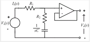
Using the concept of virtual ground, the op-amp lag compensator can be redrawn as shown in the figure
Using voltage divider principle, the transfer function of the system is
Vo/Vs=(1+s*C*R1)/(1+(R1*R2/(R1+R2))*s*C),
Hence the phase added to system is given as
Ω =tan-1(ω*C*R1) -tan-1(ω*C*R1*R2/(R1+R2)).
Since R1 > R1*R2/(R1+R2) Ω is positive(phase lead).
Q11) Explain integrator using op-amp?
A11)

Since the non-inverting input terminal of op-amp is grounded v2=0. Due to virtual short at the input of op-amp the inverting and non-inverting input terminals are at the same potential
Therefore v1=v2=0
Due to high impedance of op-amp the current flowing into its input terminal is zero. Therefore the same current flows through R and C
That is
i1 = if -------------------(1)
Where i1 = vi – v1 /R = vi -/R---------------------(2)
And if = C d/dt[v1 – v0] = -C dv0/dt --------------------(3)
Substituting (2) and (3) in (1) we get
Vi = - C/R dv0/dt ------------------------(4)
Dvo/dt = (-1/RC) vi ---------------------------- (5)
Integrating both sides of eq(5) we get
v0 = - 1/RC  + v0(0) --------------------------(6)
Where v0(0) is the initial voltage on the capacitor at t=0.
Note: v0(o) represents the constant of integration.
From eq(6) we find that the output voltage is proportional to the integral of the input voltage.
Therefore v0 = - 1/RC 

Q12) The integrator circuit as shown in the figure has R = 500K Ω and C=1µF. Find and plot the output voltage for the inputs as shown in the figure.

c)vi= 2 sin 4tVd) vi= 4tV
A12)
We know that
v0 = - 1/RC  + v0(0)
Here R= 500K Ω and C = 1µF
1/RC = 1/ 500 x 1000 x 1 x 10-6
= 1/RC = 2
= -2  ; vi =- 5V
= -2 
= 10t V
Which means it is a ramp voltage with positive slope.
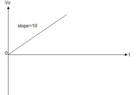
When vi=5V
-2  ; vi = 5V
= -2 
= -10t V
Which means it is a ramp voltage with negative slope.
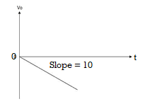
When vi= 2 sin4t V
Vo = -2 
= -4 [-cos 4t] /4 cos 4t

When vi=4t V
Vo = 
= -8 [t2/2]
= - 4V

Q13) Explain the working of regulator?
A13)
By utilizing an op-amp and few other external components, linear voltage regulator is built The same circuit is also a voltage stabilizer, able to stabilize voltage at a grade better than The transistor is used to supply the load with much more current than the op-amp itself could possibly supply.
The D1 diode is a Zener -type diode and it is used for voltage reference.

Fig. Basic op-amp voltage regulator
D1 is biased through Rz. When correctly reserve biased, the Zener diode keeps the voltage across its leads close to the Zener breakdown voltage. The op-amp is used as a linear voltage amplifier.
Due to the high open loop voltage gain of the op-amp the op-amp remains in its linear region, the voltage difference between its inverting (V-) and non-inverting input (V+) is almost equal to zero.
In other words, the voltage at its non-inverting input, in respect to the ground, equals the voltage at its inverting input:
V-=V+ -------(1)
Equation (1) holds true for any op-amp working at its linear region (as an amplifier).
R1 and R2 form a voltage divider, and the voltage (V-) at their connection point is also given by the well- known voltage-divider formula:
V-=VL·R1/(R1+R2) ------ (2)
However, V+ is also equal to the Zener breakdown voltage (Vz), because the non-inverting input of the op-amp is directly connected to the cathode of the Zener diode.
V+=VZ -----------------(3)
After solving (1),(2) and (3), we get:
VL=VZ·(1+R2/R1) --------------(4)
From equation (4), we conclude that VL voltage which is the voltage applied to the load is directly proportional to the Zener voltage.
As long as Zener voltage remains stable, VL also remains stable. Additionally, the voltage applied to the load, can be easily adjusted by adjusting R1, R2 or both. For continues voltage adjustment, R1 and R2 can be replaced by a potentiometer, having its wiper at the non-inverting input of the op-amp, and its other leads at the ground and the VL line, respectively.
Q14) Explain Wein bridge oscillator?
A14)
Wien bridge oscillator is an audio frequency sine wave oscillator of high stability and simplicity. The feedback signal in this circuit is connected to the non-inverting input terminal so that the op-amp is working as a non-inverting amplifier.
The feedback network does not provide any phase shift. The circuit can be viewed as a Wien bridge with a series combination of R1 and C1 in one arm and parallel combination of R2 and C2 in the adjoining arm. Resistors R3 and R4 are connected in the remaining two arms.
The condition of zero phase shift around the circuit is achieved by balancing the bridge. The series and parallel combination of RC network form a lead-lag circuit.
At high frequencies, the reactance of capacitor C1 and C2 approaches zero. This causes C1 and C2 appears short. Here, capacitor C2 shorts the resistor R2. Hence, the output voltage Vo will be zero since output is taken across R2 and C2 combination. So, at high frequencies, circuit acts as a 'lag circuit'.
At low frequencies, both capacitors act as open because capacitor offers very high reactance. Again, output voltage will be zero because the input signal is dropped across the R1 and C1 combination. Here, the circuit acts like a 'lead circuit'.
But at one particular frequency between the two extremes, the output voltage reaches to the maximum value. At this frequency only, resistance value becomes equal to capacitive reactance and gives maximum output. Hence, this frequency is known as oscillating frequency (f).
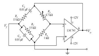

Consider the feedback circuit, on applying voltage divider rule
Vf(s) = Vo(s) x Zp(s)/ Zp(s) + Zs(s)
Zs(s) = R1 + 1/sC1 and Zp(s) = R2|| 1/sC2
Let R1=R2=R and C1=C2=C . On solving
β = Vf(s)/ Vo(s) = RsC /(RsC) 2 + 3RsC + 1 ---------------------------(1)
Since the op-amp is operated in the non-inverting configuration the voltage gain
Av = Vo(s)/ Vf(s) = 1 + R3/R4 -------------------(2)
Applying the condition for sustained oscillations, = Av β =1
RsC /(RsC) 2 + 3RsC + 1. 1 + R3/R4
S=jw
(1 + R3/R4) ( jwRC/ - R2 C2 w2 + 3 jwRC + 1) =1
Jw RC (1 + R3/R4)= (- R2 C2 w2 + 3 jwRC + 1)
Jw[(1 + R3/R4)RC – 3RC] = 1- R2 C2 w2
To obtain the frequency of oscillation equate the real part to zero
1 - R2 C2 w2 = 0
w = 1/RC
f = 1/ 2 π RC
To obtain the condition for gain at the frequency of oscillation equate the imaginary part to zero.
Jw[(1 + R3/R4)RC – 3RC] = 0
jw[(1 + R3/R4)RC= jw3RC
[(1 + R3/R4) =3
R3/R4 =2
Therefore R3 = 2 R4 is the required condition.
Q15) Explain phase shift oscillator?
A15)
Phase Shift oscillator

In an RC Oscillator circuit, the input is shifted 180o through the feedback circuit returning the signal out-of-phase and 180o again through an inverting amplifier stage to produces the required positive feedback.
This then gives us “180o + 180o = 360o” of phase shift which is effectively the same as 0o, thereby giving us the required positive feedback.
In other words, the total phase shift of the feedback loop should be “0” or any multiple of 360o to obtain the same effect.

The circuit on the left shows a single resistor-capacitor network whose output voltage “leads” the input voltage by some angle less than 90o.
In a pure or ideal single-pole RC network. It would produce a maximum phase shift of exactly 90o, and because 180o of phase shift is required for oscillation, at least two single-poles networks must be used within an RC oscillator design.
However, in reality it is difficult to obtain exactly 90o of phase shift for each RC stage so we must therefore use more RC stages cascaded together to obtain the required value at the oscillation frequency.
The amount of actual phase shift in the circuit depends upon the values of the resistor (R) and the capacitor (C), at the chosen frequency of oscillations with the phase angle ( φ ) being given as:
Xc = 1/2π fc R=R
Z = [ R 2 + Xc 2 ] ½
Ø = tan -1 Xc /R
Q16) Explain analog to digital converter?
A16)
Analog to digital converter samples the analog signal on each falling or rising edge of sample clock. In each cycle, the ADC gets of the analog signal, measures and converts it into a digital value. The ADC converts the output data into a series of digital values by approximates the signal with fixed precision.
In ADCs, two factors determine the accuracy of the digital value that captures the original analog signal. These are quantization level or bit rate and sampling rate.
The figure depicts how analog to digital conversion takes place. Bit rate decides the resolution of digitized output
The figure displays 3-bit ADC is used for converting analog signal.

Assume that one volt signal has to be converted from digital by using 3-bit ADC as shown below. Therefore, a total of 2^3=8 divisions are available for producing 1V output. This results 1/8=0.125V is called as minimum change or quantization level represented for each division as 000 for 0V, 001 for 0.125, and likewise upto 111 for 1V. If we increase the bit rates like 6, 8, 12, 14, 16, etc. we will get a better precision of the signal. Thus, bit rate or quantization gives the smallest output change in the analog signal value that results from a change in the digital representation.
Q17) Explain hysteresis comparator?
A17)
A hysteresis comparator is operated by applying positive feedback to the comparator. The potential difference between High and Low output voltages and the feedback resistor are adjusted to change the voltage that is taken as a comparison reference to the input voltage for +IN terminal. The width of variation in the reference voltage is the hysteresis width. In this circuit the signal to -IN terminal and the output is inverted.

Q18) Explain its operation with hysteresis?
A18)
Operation with hysteresis:
Since a margin is provided between the High-to-Low and Low-to-High thresholds, no chattering occurs in the output even when a signal is input at a voltage near the threshold voltages.

When the input signal (-IN) is applied at a voltage sufficiently higher than VthH(+IN) and VthL(+IN), the output is varied according to Vref as a threshold.
When the input signal (-IN) is applied at a voltage equivalent to VthH(+IN) or above, no chattering occurs since the output will not respond unless the input falls below the threshold at VthL(+IN).
VthL is the voltage switching from Low to High.
VthH is the voltage switching from High to Low.
Q19) Explain zero crossing detector?
A19)
An op-amp detector that has the ability to detect the change from positive to negative or negative to a positive level of a sinusoidal waveform is known as a zero- crossing detector.
It is also known to be a square wave generator as the applied input signal is converted into a square wave by the zero -crossing detector.

Here, the input signal Vi is provided to the inverting terminal of the op-amp while the non-inverting terminal is grounded by making use of two resistors R1 and R2.
It detects the point where the input signal crosses zero of the reference voltage level. For every crossing, the saturation level of the output signal changes from one to another.
The reference level is set at 0 and applied at the non-inverting terminal of the op-amp. The sine wave applied at the inverting terminal of the op-amp is compared with the reference level each time the phase of the wave changes either from positive to negative or negative to positive.
Firstly, when positive half of the sinusoidal signal appears at the input. Then the op-amp comparator compares the reference voltage level with the peak level of the applied signal.
Vo = Vref – Vi ---------------------------------------(1)
And we know the reference level is 0, thus
Vo = 0 – ( + Vsat) ----------------------------------------(2)
Therefore, Vo = - Vsat ---------------------------------(3)
During the negative half of the signal, thus the peak will have a negative polarity.
Again
Vo = Vref – Vi ---------------------------------------------(4)
Thus,
Vo = 0 - ( - Vsat) --------------------------------------------------(5)
So, we get
Vo = + Vsat ---------------------------------------------(6)
In this way, the zero -crossing detector detects the change in the level of the applied signal.
Zero crossing detector is also known to be a square wave generator. As the output of the window comparator is nothing but a square wave.

V0 for the positive half of the applied signal is – Vsat,
This is the reason why we have achieved negative half of the square wave at the output when positive half of the sinusoidal signal is applied. While V0 for the negative half of the sinusoidal signal is + Vsat,
Q20) Explain square wave generator?
A20)
Square wave generator
The square wave generator is based on a uA741 opamp (IC1). Resistor R1 and capacitor C1 determines the frequency of the square wave. Resistor R2 and R3 forms a voltage divider setup which feedbacks a fixed fraction of the output to the non-inverting input of the IC.
- Initially, when power is not applied the voltage across the capacitor C1 is 0. When the power supply is switched ON, the C1 starts charging through the resistor R1 and the output of the op-amp will be high.
- A fraction of this high voltage is fed back to the non- inverting pin by the resistor network R2, R3. When the voltage across the charging capacitor is increased to a point the voltage at the inverting pin is higher than the non-inverting pin, the output of the op-amp swings to negative saturation (-Vcc).
- The capacitor quickly discharges through R1 and starts charging in the negative direction again through R1.
- Fraction of the negative high output (-Vcc) is fed back to the non-inverting pin by the feedback network R2, R3. When the voltage across the capacitor has become so negative that the voltage at the inverting pin is less than the voltage at the non-inverting pin, the output of the op-amp swings back to the positive saturation.
- Now the capacitor discharges trough R1 and starts charging in positive direction. This cycle is repeated over time and the result is a square wave swinging between +Vcc and -Vcc at the output of the op-amp.
If the values of R2 and R3 are made equal, then the frequency of the square wave can be expressed using the following equation
F = 1/(2.1976 R1C1)
Q21) Explain triangular wave generator?
A21)
The op-amp IC used in this stage is also uA741 (IC2). Resistor R5 in conjunction with R4 sets the gain of the integrator and resistor R5 in conjunction with C2 sets the bandwidth. The square wave signal is applied to the inverting input of the op-amp through the input resistor R4. The op-amp integrator part of the circuit is shown in the figure below.

After this initial “kick” the capacitor starts charging and it creates an opposition to the input current flowing through the input resistor R4. The negative feedback compels the op-amp to produce a voltage at its out so that it maintains the virtual ground at the inverting input.
Since the capacitor is charging its impedance Xc keeps increasing and the gain Xc2/R4 also keeps increasing. This results in a ramp at the output of the op-amp that increases in a rate proportional to the RC time constant (T=R4C2) and this ramp increases in amplitude until the capacitor is fully charged.
When the input to the integrator (square wave) falls to the negative peak the capacitor quickly discharges through the input resistor R4 and starts charging in the opposite polarity.
Now the conditions are reversed, and the output of the op-amp will be a ramp that is going to the negative side at a rate proportional to the R4R2 time constant. This cycle is repeated, and the result will be a triangular waveform at the output of the op-amp integrator.
Q22) Explain precision rectifier?
A22)
A rectifier is a circuit that converts alternating current (AC) to Direct current (DC). An alternating current always changes its direction over time, but the direct current flows continuously in one direction.
In a typical rectifier circuit, we use diodes to rectify AC to DC. But this rectification method can only be used if the input voltage to the circuit is greater than the forward voltage of the diode which is typically 0.7V.
The precision rectifier is another rectifier that converts AC to DC, but in a precision rectifier we use an op-amp to compensate for the voltage drop across the diode, that is why we are not losing the 0.6V or 0.7V voltage drop across the diode, also the circuit can be constructed to have some gain at the output of the amplifier as well.
Q23) Explain half-wave precision rectifier?
A23)

Fig. Half wave precision rectifier circuit
The input and output waveform of the precision rectifier circuit, which is exactly equal to the input. That's because we are taking the feedback from the output of the diode and the op-amp compensates for any voltage drop across the diode. So, the diode behaves like an ideal diode.
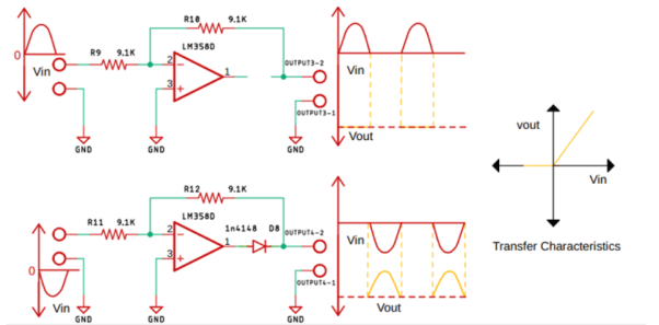
Fig. When positive and negative half cycle of input signal is applied to Op-amp
Q24) Explain peak detector?
A24)
Peak detector circuits are used to determine the peak (maximum) value of an input signal. It stores the peak value of input voltages for infinite time duration until it comes to reset condition.
The peak detector circuit utilizes its property of following the highest value of an input signal and storing it.
Rectifier circuits usually provide an output in proportion to the average value of the input. However, some application requires measurement of the peak value of the signal. Thus, peak detectors are used. Usually, the peak of non-sinusoidal waveforms is measured using a peak detector.

The peak of the input waveform is followed and stored in terms of voltage in the capacitor. If the circuit detects a higher peak, the new peak value is stored in the capacitor until it is discharged.
The capacitor employed in the circuit is charged through the diode by the applied input signal. The small voltage drop across the diode is ignored and the capacitor is charged up to the highest peak of the applied input signal.
Let us consider initially the capacitor is charged to voltage Vc. The diode employed in the circuit gets forward biased when the applied input voltage Vin exceeds the capacitor voltage Vc. Thereby allowing the circuit to behave as a voltage follower. The output voltage follows the applied input voltage until Vin is more than Vc.
As the input voltage Vin reduces below the value of capacitive voltage Vc, it causes the diode to get reverse biased. In such condition, the capacitor retains the value until the input again exceeds the value stored in the capacitor.
Q25) What is monoshot?
A25)
A monostable multivibrator has a “stable” state (say, Vo = 0 V) and a “transient” state (say, Vo = Vhigh). Consider the circuit to be in the stable state in the beginning.
When a certain “event” occurs, it enters the transient state, remains in that state for a time interval T, and then returns to its stable state.
Fig. (a) shows an implementation of the monostable multivibrator circuit using the Schmitt trigger of Figure.
Assume that the circuit is in the stable state in the beginning the capacitor has charged to +V ′ − (−V ′ ) = 2V ′ , the input voltage V− for the Schmitt trigger (with respect to ground) is Vo = −Vm (with Vm = VZ + Von).
And V+ = −Vm R1 R1 + R2 see Figs. (c) and (d). At t = t1, capacitor discharges and VC becomes 0 V, V− changes to −V ′, and the output Vo to +Vm.
When the capacitor starts charging since the input current of the op amp is negligibly small, the charging process can be described by
V−(t) = A e−(t−t1)/τ + B, for t > t1 , where τ = RC.
Using V−(t1) = −V ′ and V (∞) = +V ′, we get A = −2V ′ , B = V ′ ,
i.e., V−(t) = V ′ (1 − 2e −(t−t1)/τ ).
When V− crosses VT H, the output changes to +Vm (at t = t1 + T in Fig. (c).
The capacitor continues to charge, and in about five-time constants, we have once again the original stable state that we started with at t = 0.
To calculate T, we simply substitute V−(t1 + T) = VT H in Eq. and obtain
VT H = V ′ (1 − 2 e −T /τ ) → T = RC × log (2 V ′ /V ′ − VT H ).
Unit - 5
Unit - 5
Linear & Nonlinear applications of op-amp
Q1) Explain the idealised analysis of op-amp circuits?
A1)
An Operational Amplifier is basically a three-terminal device which consists of two high impedance inputs. One of the inputs is called the Inverting Input, marked with a negative or “minus” sign, ( – ). The other input is called the Non-inverting Input, marked with a positive or “plus” sign ( + ).
A third terminal represents the operational amplifiers output port which can both sink and source either a voltage or a current.
In a linear operational amplifier, the output signal is the amplification factor, known as the amplifiers gain ( A ) multiplied by the value of the input signal and depending on the nature of these input and output signals, there can be four different classifications of operational amplifier gain.
- Voltage – Voltage “in” and Voltage “out”
- Current – Current “in” and Current “out”
- Transconductance – Voltage “in” and Current “out”
- Transresistance – Current “in” and Voltage “out”
Q2) Explain the important characteristics of op-amp?
A2)
Open Loop Gain (Avo)
The main function of an operational amplifier is to amplify the input signal and the more open loop gain it has the better. Open-loop gain is the gain of the op-amp without positive or negative feedback and for such an amplifier the gain will be infinite
Input impedance (ZIN)
Input impedance is the ratio of input voltage to input current and is assumed to be infinite to prevent any current flowing from the source supply into the amplifiers input circuitry ( IIN = 0 ). Real op-amps have input leakage currents from a few pico-amps to a few milli-amps.
Output impedance (ZOUT)
The output impedance of the ideal operational amplifier is assumed to be zero acting as a perfect internal voltage source with no internal resistance so that it can supply as much current as necessary to the load.
This internal resistance is effectively in series with the load thereby reducing the output voltage available to the load. Real op-amps have output impedances in the 100-20kΩ range.
Bandwidth (BW)
An ideal operational amplifier has an infinite frequency response and can amplify any frequency signal from DC to the highest AC frequencies, so it is therefore assumed to have an infinite bandwidth.
With real op-amps, the bandwidth is limited by the Gain-Bandwidth product (GB), which is equal to the frequency where the amplifiers gain becomes unity.
Offset Voltage (VIO)
The amplifiers output will be zero when the voltage difference between the inverting and the non-inverting inputs is zero, the same or when both inputs are grounded. Real op-amps have some amount of output offset voltage.
Q3) Explain inverting and non-inverting amplifier?
A3)
Inverting Amplifier
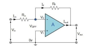
The input signal vi is applied to the inverting input terminal through resistor R1 and non-inverting input terminal is grounded. The feedback from the output of the inverting terminal is provided through the feedback resistor Rf.
Since the input is applied to the inverting terminal vo and vi are opposite in polarity and hence the feedback is negative. Since the non-inverting input terminal is grounded v2=0. Due to virtual short at the input of op-amp the inverting and non-inverting input terminals are at the same potential.
Therefore, v1 = v2 = 0.
Due to high input impedance of Op-amp the current flowing into its inverting input terminal is zero. Therefore, the same current flows through R1 and Rf .
i 1 = i f
But i1 = vi – v1 / R1 = vi/R1
i f = v1 – vo / Rf = -vo/Rf
Vi/R1 = - vo/Rf
Af = vo/vi = -Rf/R1
Af is the closed loop voltage gain or voltage gain with negative feedback.
Non-inverting amplifier
Non- Inverting amplifier is one in which the output is in phase with respect to input that is if you apply a positive voltage, output will be positive. The output is an non -inverted amplified version of input.
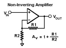
Assuming the op-amp is ideal and applying the concept of virtual short, the voltage at the inverting terminal is equal to non- inverting terminal.
Applying KCL at inverting node we get
Vi -Vo/ R2 + Vo – 0 / R1 = 0
By rearranging the terms, we will get
Voltage gain Av = Vo/ Vi = (1+ Rf/Ri)
Gain of non- inverting amplifier Av= (1+ Rf/Ri).
Q4) Explain differential amplifier?
A4)
The differential amplifier amplifies the difference between two voltages making this type of operational amplifier circuit a Subtractor This type of operational amplifier circuit is commonly known as a Differential Amplifier.

By connecting each input in turn to 0v ground we can use superposition to solve for the output voltage Vout. Then the transfer function for a Differential Amplifier circuit is given as:
I1 = V1-Va/R1 ; I2 = V2-Vb/R2 ; If = Va –(Vout)/R3
Summing Point Va =Vb
Vb = V2(R4/R2+R4)
If V2 =0 then Vout = -V1 (R3/R1)
If V1=0 then Vout = V2(R4/R2+R4)(R1+R3/R1)
Vout = -Vout (a) + Vout(b)
Vout = -V1(R3/R1) + V2(R4/R2+R4)(R1+R3/R1)
When resistors, R1 = R2 and R3 = R4 the above transfer function for the differential amplifier can be simplified to the following expression:
Vout = (V2 -V1)
The output is the difference between the two inputs hence, the op-amp can be used as subtractor.
Q5) Explain instrumentation amplifier?
A5)
The Instrumentation amplifiers consist of three op-amps. In this circuit, a non-inverting amplifier is connected to each input of the differential amplifier.
This instrumentation amplifier provides high input impedance for exact measurement of input data from transducers. The circuit diagram of an instrumentation amplifier is as shown in the figure below.

The op-amps 1 & 2 are non-inverting amplifiers and together form an input stage of the instrumentation amplifier. The op-amp 3 is a difference amplifier that forms the output stage of the instrumentation amplifier.
Working
The output stage of the instrumentation amplifier is a difference amplifier, whose output Vout is the amplified difference of the input signals applied to its input terminals.
If the outputs of op-amp 1 and op-amp 2 are Vo1 and Vo2 respectively, then the output of the difference amplifier is given by,
Vout = (R3/R2)(Vo1-Vo2)
The expressions for Vo1 and Vo2 can be found in terms of the input voltages and resistances.
Consider the input stage of the instrumentation amplifier as shown in the figure below.

The potential at node A is the input voltage V1. Hence the potential at node B is also V1, from the virtual short concept. Thus, the potential at node G is also V1.
The potential at node D is the input voltage V2. Hence the potential at node C is also V2, from the virtual short. Thus, the potential at node H is also V2.
Ideally the current to the input stage op-amps is zero. Therefore, the current I through the resistors R1, Rgain and R1 remains the same.
Applying Ohm’s law between the nodes E and F,
I = (Vo1-Vo2)/(R1+Rgain+R1) ——————— 1
I = (Vo1-Vo2)/(2R1+Rgain)
Since no current is flowing to the input of the op-amps 1 & 2, the current I between the nodes G and H can be given as,
I = (VG-VH)/Rgain = (V1-V2)/Rgain ————————- 2
Equating equations 1 and 2,
(Vo1-Vo2)/(2R1+Rgain) = (V1-V2)/Rgain
(Vo1-Vo2) = (2R1+Rgain)(V1-V2)/Rgain —————— 3
The output of the difference amplifier is given as,
Vout = (R3/R2) (Vo1-Vo2)
Therefore, (Vo1 – Vo2) = (R2/R3)Vout
Substituting (Vo1 – Vo2) value in the equation 3, we get
(R2/R3)Vout = (2R1+Rgain)(V1-V2)/Rgain
i.e. Vout = (R3/R2){(2R1+Rgain)/Rgain}(V1-V2)
The above equation gives the output voltage of an instrumentation amplifier. The overall gain of the amplifier is given by the term (R3/R2){(2R1+Rgain)/Rgain}.
Q6) Write a short note on active filters?
A6)
Active filters are the electronic circuits, which consist of active element like op-amp(s) along with passive elements like resistor(s) and capacitor(s).
Active filters are mainly classified into the following four types based on the band of frequencies that they are allowing and / or rejecting −
- Active Low Pass Filter
- Active High Pass Filter
- Active Band Pass Filter
- Active Band Stop Filter
Q7) Explain P controller?
A7)
P Control
The Output power is directly proportional to control error. The higher the proportion coefficient, the less the output power at the same control error
Proportional control is mainly for fast-response systems with a large transmission coefficient. To adjust the proportional controller first set the maximum proportion coefficient where in the output power decreases to zero.
When the measured value is stabilized, set a specified value and gradually reduce the proportion coefficient and the control error will decrease.
If there are periodic oscillations in the system, the proportion coefficient should be increased so that control error is minimal periodic oscillations decrease to the limit.
Q8) Explain PI control?
A8)
The Output power equals to the sum of proportion and integration coefficients. The higher the proportion coefficient, the less the output power at the same control error. The higher the integration coefficient, the slower the accumulated integration coefficient.
PI control provides zero control error and and is insensitive to interference of the measurement channel. The PI control disadvantage is slow reaction to disturbances.
To adjust the PI controller first set the integration time equal to zero, and the maximum proportion time. Then by decreasing the coefficient of proportionality, achieve periodic oscillations in the system.
Q9) Explain PID control?
A9)
The Output power equals to the sum of three coefficients: proportional, integral and differential. The higher the proportion coefficient, the less the output power at the same control error.
The higher the integration coefficient, the slower the accumulated integration coefficient. The higher the differentiation coefficient, the greater the response of the system to the disturbance.
The PID controller is used in inertial systems with relatively low noise level of the measuring channel.
The advantage of PID is fast warm up time, accurate setpoint temperature control and fast reaction to disturbances.
Q10) Explain lead/lag compensator using op-amp
A10)
Lag compensator
A lag compensator is one which adds a pole to the system and is used to improve the steady state response of the system. A lag compensator provides phase lag negative phase in the frequency response of system.

Using the concept of virtual ground, the op-amp lag compensator can be redrawn as shown in the figure
Using voltage divider principle, the transfer function of the system is
Vo/Vs =(1+s*C*R1)/(1+(R1+R2)*s*C),
Hence the phase added to system is given as
Ω = tan-1(ω*C*R1) – tan-1(ω*C*(R1+R2))
Since R1<R1+R2 and tan-1(x) is increasing function (if a <b, tan-1(a)< tan1(b)) Ω is negative phase lag.
Lead compensator
A lead compensator is one which adds a zero the system and is used to improve the transient response of the system. A lead compensator provides phase lead positive phas) in the frequency response of system

Using the concept of virtual ground, the op-amp lag compensator can be redrawn as shown in the figure
Using voltage divider principle, the transfer function of the system is
Vo/Vs=(1+s*C*R1)/(1+(R1*R2/(R1+R2))*s*C),
Hence the phase added to system is given as
Ω =tan-1(ω*C*R1) -tan-1(ω*C*R1*R2/(R1+R2)).
Since R1 > R1*R2/(R1+R2) Ω is positive(phase lead).
Q11) Explain integrator using op-amp?
A11)

Since the non-inverting input terminal of op-amp is grounded v2=0. Due to virtual short at the input of op-amp the inverting and non-inverting input terminals are at the same potential
Therefore v1=v2=0
Due to high impedance of op-amp the current flowing into its input terminal is zero. Therefore the same current flows through R and C
That is
i1 = if -------------------(1)
Where i1 = vi – v1 /R = vi -/R---------------------(2)
And if = C d/dt[v1 – v0] = -C dv0/dt --------------------(3)
Substituting (2) and (3) in (1) we get
Vi = - C/R dv0/dt ------------------------(4)
Dvo/dt = (-1/RC) vi ---------------------------- (5)
Integrating both sides of eq(5) we get
v0 = - 1/RC  + v0(0) --------------------------(6)
Where v0(0) is the initial voltage on the capacitor at t=0.
Note: v0(o) represents the constant of integration.
From eq(6) we find that the output voltage is proportional to the integral of the input voltage.
Therefore v0 = - 1/RC 
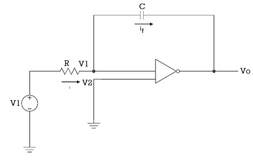
Q12) The integrator circuit as shown in the figure has R = 500K Ω and C=1µF. Find and plot the output voltage for the inputs as shown in the figure.
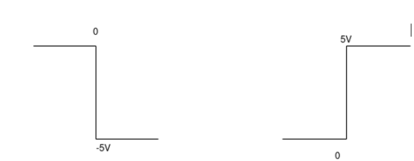
c)vi= 2 sin 4tVd) vi= 4tV
A12)
We know that
v0 = - 1/RC  + v0(0)
Here R= 500K Ω and C = 1µF
1/RC = 1/ 500 x 1000 x 1 x 10-6
= 1/RC = 2
= -2  ; vi =- 5V
= -2 
= 10t V
Which means it is a ramp voltage with positive slope.

When vi=5V
-2  ; vi = 5V
= -2 
= -10t V
Which means it is a ramp voltage with negative slope.

When vi= 2 sin4t V
Vo = -2 
= -4 [-cos 4t] /4 cos 4t

When vi=4t V
Vo = 
= -8 [t2/2]
= - 4V

Q13) Explain the working of regulator?
A13)
By utilizing an op-amp and few other external components, linear voltage regulator is built The same circuit is also a voltage stabilizer, able to stabilize voltage at a grade better than The transistor is used to supply the load with much more current than the op-amp itself could possibly supply.
The D1 diode is a Zener -type diode and it is used for voltage reference.

Fig. Basic op-amp voltage regulator
D1 is biased through Rz. When correctly reserve biased, the Zener diode keeps the voltage across its leads close to the Zener breakdown voltage. The op-amp is used as a linear voltage amplifier.
Due to the high open loop voltage gain of the op-amp the op-amp remains in its linear region, the voltage difference between its inverting (V-) and non-inverting input (V+) is almost equal to zero.
In other words, the voltage at its non-inverting input, in respect to the ground, equals the voltage at its inverting input:
V-=V+ -------(1)
Equation (1) holds true for any op-amp working at its linear region (as an amplifier).
R1 and R2 form a voltage divider, and the voltage (V-) at their connection point is also given by the well- known voltage-divider formula:
V-=VL·R1/(R1+R2) ------ (2)
However, V+ is also equal to the Zener breakdown voltage (Vz), because the non-inverting input of the op-amp is directly connected to the cathode of the Zener diode.
V+=VZ -----------------(3)
After solving (1),(2) and (3), we get:
VL=VZ·(1+R2/R1) --------------(4)
From equation (4), we conclude that VL voltage which is the voltage applied to the load is directly proportional to the Zener voltage.
As long as Zener voltage remains stable, VL also remains stable. Additionally, the voltage applied to the load, can be easily adjusted by adjusting R1, R2 or both. For continues voltage adjustment, R1 and R2 can be replaced by a potentiometer, having its wiper at the non-inverting input of the op-amp, and its other leads at the ground and the VL line, respectively.
Q14) Explain Wein bridge oscillator?
A14)
Wien bridge oscillator is an audio frequency sine wave oscillator of high stability and simplicity. The feedback signal in this circuit is connected to the non-inverting input terminal so that the op-amp is working as a non-inverting amplifier.
The feedback network does not provide any phase shift. The circuit can be viewed as a Wien bridge with a series combination of R1 and C1 in one arm and parallel combination of R2 and C2 in the adjoining arm. Resistors R3 and R4 are connected in the remaining two arms.
The condition of zero phase shift around the circuit is achieved by balancing the bridge. The series and parallel combination of RC network form a lead-lag circuit.
At high frequencies, the reactance of capacitor C1 and C2 approaches zero. This causes C1 and C2 appears short. Here, capacitor C2 shorts the resistor R2. Hence, the output voltage Vo will be zero since output is taken across R2 and C2 combination. So, at high frequencies, circuit acts as a 'lag circuit'.
At low frequencies, both capacitors act as open because capacitor offers very high reactance. Again, output voltage will be zero because the input signal is dropped across the R1 and C1 combination. Here, the circuit acts like a 'lead circuit'.
But at one particular frequency between the two extremes, the output voltage reaches to the maximum value. At this frequency only, resistance value becomes equal to capacitive reactance and gives maximum output. Hence, this frequency is known as oscillating frequency (f).


Consider the feedback circuit, on applying voltage divider rule
Vf(s) = Vo(s) x Zp(s)/ Zp(s) + Zs(s)
Zs(s) = R1 + 1/sC1 and Zp(s) = R2|| 1/sC2
Let R1=R2=R and C1=C2=C . On solving
β = Vf(s)/ Vo(s) = RsC /(RsC) 2 + 3RsC + 1 ---------------------------(1)
Since the op-amp is operated in the non-inverting configuration the voltage gain
Av = Vo(s)/ Vf(s) = 1 + R3/R4 -------------------(2)
Applying the condition for sustained oscillations, = Av β =1
RsC /(RsC) 2 + 3RsC + 1. 1 + R3/R4
S=jw
(1 + R3/R4) ( jwRC/ - R2 C2 w2 + 3 jwRC + 1) =1
Jw RC (1 + R3/R4)= (- R2 C2 w2 + 3 jwRC + 1)
Jw[(1 + R3/R4)RC – 3RC] = 1- R2 C2 w2
To obtain the frequency of oscillation equate the real part to zero
1 - R2 C2 w2 = 0
w = 1/RC
f = 1/ 2 π RC
To obtain the condition for gain at the frequency of oscillation equate the imaginary part to zero.
Jw[(1 + R3/R4)RC – 3RC] = 0
jw[(1 + R3/R4)RC= jw3RC
[(1 + R3/R4) =3
R3/R4 =2
Therefore R3 = 2 R4 is the required condition.
Q15) Explain phase shift oscillator?
A15)
Phase Shift oscillator

In an RC Oscillator circuit, the input is shifted 180o through the feedback circuit returning the signal out-of-phase and 180o again through an inverting amplifier stage to produces the required positive feedback.
This then gives us “180o + 180o = 360o” of phase shift which is effectively the same as 0o, thereby giving us the required positive feedback.
In other words, the total phase shift of the feedback loop should be “0” or any multiple of 360o to obtain the same effect.

The circuit on the left shows a single resistor-capacitor network whose output voltage “leads” the input voltage by some angle less than 90o.
In a pure or ideal single-pole RC network. It would produce a maximum phase shift of exactly 90o, and because 180o of phase shift is required for oscillation, at least two single-poles networks must be used within an RC oscillator design.
However, in reality it is difficult to obtain exactly 90o of phase shift for each RC stage so we must therefore use more RC stages cascaded together to obtain the required value at the oscillation frequency.
The amount of actual phase shift in the circuit depends upon the values of the resistor (R) and the capacitor (C), at the chosen frequency of oscillations with the phase angle ( φ ) being given as:
Xc = 1/2π fc R=R
Z = [ R 2 + Xc 2 ] ½
Ø = tan -1 Xc /R
Q16) Explain analog to digital converter?
A16)
Analog to digital converter samples the analog signal on each falling or rising edge of sample clock. In each cycle, the ADC gets of the analog signal, measures and converts it into a digital value. The ADC converts the output data into a series of digital values by approximates the signal with fixed precision.
In ADCs, two factors determine the accuracy of the digital value that captures the original analog signal. These are quantization level or bit rate and sampling rate.
The figure depicts how analog to digital conversion takes place. Bit rate decides the resolution of digitized output
The figure displays 3-bit ADC is used for converting analog signal.

Assume that one volt signal has to be converted from digital by using 3-bit ADC as shown below. Therefore, a total of 2^3=8 divisions are available for producing 1V output. This results 1/8=0.125V is called as minimum change or quantization level represented for each division as 000 for 0V, 001 for 0.125, and likewise upto 111 for 1V. If we increase the bit rates like 6, 8, 12, 14, 16, etc. we will get a better precision of the signal. Thus, bit rate or quantization gives the smallest output change in the analog signal value that results from a change in the digital representation.
Q17) Explain hysteresis comparator?
A17)
A hysteresis comparator is operated by applying positive feedback to the comparator. The potential difference between High and Low output voltages and the feedback resistor are adjusted to change the voltage that is taken as a comparison reference to the input voltage for +IN terminal. The width of variation in the reference voltage is the hysteresis width. In this circuit the signal to -IN terminal and the output is inverted.
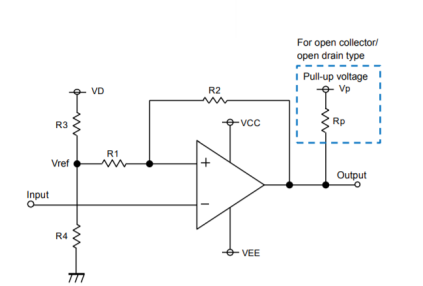
Q18) Explain its operation with hysteresis?
A18)
Operation with hysteresis:
Since a margin is provided between the High-to-Low and Low-to-High thresholds, no chattering occurs in the output even when a signal is input at a voltage near the threshold voltages.
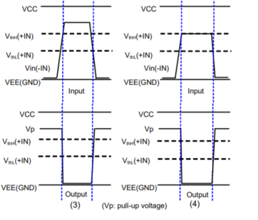
When the input signal (-IN) is applied at a voltage sufficiently higher than VthH(+IN) and VthL(+IN), the output is varied according to Vref as a threshold.
When the input signal (-IN) is applied at a voltage equivalent to VthH(+IN) or above, no chattering occurs since the output will not respond unless the input falls below the threshold at VthL(+IN).
VthL is the voltage switching from Low to High.
VthH is the voltage switching from High to Low.
Q19) Explain zero crossing detector?
A19)
An op-amp detector that has the ability to detect the change from positive to negative or negative to a positive level of a sinusoidal waveform is known as a zero- crossing detector.
It is also known to be a square wave generator as the applied input signal is converted into a square wave by the zero -crossing detector.

Here, the input signal Vi is provided to the inverting terminal of the op-amp while the non-inverting terminal is grounded by making use of two resistors R1 and R2.
It detects the point where the input signal crosses zero of the reference voltage level. For every crossing, the saturation level of the output signal changes from one to another.
The reference level is set at 0 and applied at the non-inverting terminal of the op-amp. The sine wave applied at the inverting terminal of the op-amp is compared with the reference level each time the phase of the wave changes either from positive to negative or negative to positive.
Firstly, when positive half of the sinusoidal signal appears at the input. Then the op-amp comparator compares the reference voltage level with the peak level of the applied signal.
Vo = Vref – Vi ---------------------------------------(1)
And we know the reference level is 0, thus
Vo = 0 – ( + Vsat) ----------------------------------------(2)
Therefore, Vo = - Vsat ---------------------------------(3)
During the negative half of the signal, thus the peak will have a negative polarity.
Again
Vo = Vref – Vi ---------------------------------------------(4)
Thus,
Vo = 0 - ( - Vsat) --------------------------------------------------(5)
So, we get
Vo = + Vsat ---------------------------------------------(6)
In this way, the zero -crossing detector detects the change in the level of the applied signal.
Zero crossing detector is also known to be a square wave generator. As the output of the window comparator is nothing but a square wave.

V0 for the positive half of the applied signal is – Vsat,
This is the reason why we have achieved negative half of the square wave at the output when positive half of the sinusoidal signal is applied. While V0 for the negative half of the sinusoidal signal is + Vsat,
Q20) Explain square wave generator?
A20)
Square wave generator
The square wave generator is based on a uA741 opamp (IC1). Resistor R1 and capacitor C1 determines the frequency of the square wave. Resistor R2 and R3 forms a voltage divider setup which feedbacks a fixed fraction of the output to the non-inverting input of the IC.
- Initially, when power is not applied the voltage across the capacitor C1 is 0. When the power supply is switched ON, the C1 starts charging through the resistor R1 and the output of the op-amp will be high.
- A fraction of this high voltage is fed back to the non- inverting pin by the resistor network R2, R3. When the voltage across the charging capacitor is increased to a point the voltage at the inverting pin is higher than the non-inverting pin, the output of the op-amp swings to negative saturation (-Vcc).
- The capacitor quickly discharges through R1 and starts charging in the negative direction again through R1.
- Fraction of the negative high output (-Vcc) is fed back to the non-inverting pin by the feedback network R2, R3. When the voltage across the capacitor has become so negative that the voltage at the inverting pin is less than the voltage at the non-inverting pin, the output of the op-amp swings back to the positive saturation.
- Now the capacitor discharges trough R1 and starts charging in positive direction. This cycle is repeated over time and the result is a square wave swinging between +Vcc and -Vcc at the output of the op-amp.
If the values of R2 and R3 are made equal, then the frequency of the square wave can be expressed using the following equation
F = 1/(2.1976 R1C1)
Q21) Explain triangular wave generator?
A21)
The op-amp IC used in this stage is also uA741 (IC2). Resistor R5 in conjunction with R4 sets the gain of the integrator and resistor R5 in conjunction with C2 sets the bandwidth. The square wave signal is applied to the inverting input of the op-amp through the input resistor R4. The op-amp integrator part of the circuit is shown in the figure below.

After this initial “kick” the capacitor starts charging and it creates an opposition to the input current flowing through the input resistor R4. The negative feedback compels the op-amp to produce a voltage at its out so that it maintains the virtual ground at the inverting input.
Since the capacitor is charging its impedance Xc keeps increasing and the gain Xc2/R4 also keeps increasing. This results in a ramp at the output of the op-amp that increases in a rate proportional to the RC time constant (T=R4C2) and this ramp increases in amplitude until the capacitor is fully charged.
When the input to the integrator (square wave) falls to the negative peak the capacitor quickly discharges through the input resistor R4 and starts charging in the opposite polarity.
Now the conditions are reversed, and the output of the op-amp will be a ramp that is going to the negative side at a rate proportional to the R4R2 time constant. This cycle is repeated, and the result will be a triangular waveform at the output of the op-amp integrator.
Q22) Explain precision rectifier?
A22)
A rectifier is a circuit that converts alternating current (AC) to Direct current (DC). An alternating current always changes its direction over time, but the direct current flows continuously in one direction.
In a typical rectifier circuit, we use diodes to rectify AC to DC. But this rectification method can only be used if the input voltage to the circuit is greater than the forward voltage of the diode which is typically 0.7V.
The precision rectifier is another rectifier that converts AC to DC, but in a precision rectifier we use an op-amp to compensate for the voltage drop across the diode, that is why we are not losing the 0.6V or 0.7V voltage drop across the diode, also the circuit can be constructed to have some gain at the output of the amplifier as well.
Q23) Explain half-wave precision rectifier?
A23)

Fig. Half wave precision rectifier circuit
The input and output waveform of the precision rectifier circuit, which is exactly equal to the input. That's because we are taking the feedback from the output of the diode and the op-amp compensates for any voltage drop across the diode. So, the diode behaves like an ideal diode.

Fig. When positive and negative half cycle of input signal is applied to Op-amp
Q24) Explain peak detector?
A24)
Peak detector circuits are used to determine the peak (maximum) value of an input signal. It stores the peak value of input voltages for infinite time duration until it comes to reset condition.
The peak detector circuit utilizes its property of following the highest value of an input signal and storing it.
Rectifier circuits usually provide an output in proportion to the average value of the input. However, some application requires measurement of the peak value of the signal. Thus, peak detectors are used. Usually, the peak of non-sinusoidal waveforms is measured using a peak detector.

The peak of the input waveform is followed and stored in terms of voltage in the capacitor. If the circuit detects a higher peak, the new peak value is stored in the capacitor until it is discharged.
The capacitor employed in the circuit is charged through the diode by the applied input signal. The small voltage drop across the diode is ignored and the capacitor is charged up to the highest peak of the applied input signal.
Let us consider initially the capacitor is charged to voltage Vc. The diode employed in the circuit gets forward biased when the applied input voltage Vin exceeds the capacitor voltage Vc. Thereby allowing the circuit to behave as a voltage follower. The output voltage follows the applied input voltage until Vin is more than Vc.
As the input voltage Vin reduces below the value of capacitive voltage Vc, it causes the diode to get reverse biased. In such condition, the capacitor retains the value until the input again exceeds the value stored in the capacitor.
Q25) What is monoshot?
A25)
A monostable multivibrator has a “stable” state (say, Vo = 0 V) and a “transient” state (say, Vo = Vhigh). Consider the circuit to be in the stable state in the beginning.
When a certain “event” occurs, it enters the transient state, remains in that state for a time interval T, and then returns to its stable state.
Fig. (a) shows an implementation of the monostable multivibrator circuit using the Schmitt trigger of Figure.
Assume that the circuit is in the stable state in the beginning the capacitor has charged to +V ′ − (−V ′ ) = 2V ′ , the input voltage V− for the Schmitt trigger (with respect to ground) is Vo = −Vm (with Vm = VZ + Von).
And V+ = −Vm R1 R1 + R2 see Figs. (c) and (d). At t = t1, capacitor discharges and VC becomes 0 V, V− changes to −V ′, and the output Vo to +Vm.
When the capacitor starts charging since the input current of the op amp is negligibly small, the charging process can be described by
V−(t) = A e−(t−t1)/τ + B, for t > t1 , where τ = RC.
Using V−(t1) = −V ′ and V (∞) = +V ′, we get A = −2V ′ , B = V ′ ,
i.e., V−(t) = V ′ (1 − 2e −(t−t1)/τ ).
When V− crosses VT H, the output changes to +Vm (at t = t1 + T in Fig. (c).
The capacitor continues to charge, and in about five-time constants, we have once again the original stable state that we started with at t = 0.
To calculate T, we simply substitute V−(t1 + T) = VT H in Eq. and obtain
VT H = V ′ (1 − 2 e −T /τ ) → T = RC × log (2 V ′ /V ′ − VT H ).