Unit - 1
Binary Codes and Boolean algebra
Q1) Explain universal gates in detail.
A1)
NAND gate
It is a digital circuit which has two or more inputs and single output and it is the inversion of logical AND gate.
The truth table of 2-input NAND gate is:
A | B | Y = (A.B)’ |
0 | 0 | 1 |
0 | 1 | 1 |
1 | 0 | 1 |
1 | 1 | 0 |
Here A, B are the inputs and Y is the output of two input NAND gate. When both inputs are ‘1’, then the output, Y is ‘0’. If at least one of the input is zero, then the output, Y is ‘1’. This is just the inverse of AND operation.
The image shows the symbol of NAND gate:

Fig.: NAND gate
NAND gate works same as AND gate followed by an inverter.
Timing Diagram:

NOR gate
It is a digital circuit that has two or more inputs and a single output which is the inversion of logical OR of all inputs.
The truth table of 2-input NOR gate is:
A | B | Y = (A+B)’ |
0 | 0 | 1 |
0 | 1 | 0 |
1 | 0 | 0 |
1 | 1 | 0 |
Here A and B are the two inputs and Y is the output. If both inputs are ‘0’, then the output is ‘1’. If any one of the input is ‘1’, then the output is ‘0’. This is exactly opposite to two input OR gate operation.
The symbol of NOR gate is:

Fig.: NOR gate
NOR gate works exactly same as that of OR gate followed by an inverter.
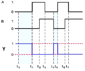
Timing Diagram:
Q2) Explain EX-OR gate and Ex-NOR gate.
A2)
Ex-OR gate
It stands for Exclusive-OR gate. Its function varies when the inputs have even number of ones.
The truth table of 2-input Ex-OR gate is:
A | B | Y = A⊕B |
0 | 0 | 0 |
0 | 1 | 1 |
1 | 0 | 1 |
1 | 1 | 0 |
Here A, B are the inputs and Y is the output of two input Ex-OR gate. The output (Y) is zero instead of one when both the inputs are one.
Therefore, the output of Ex-OR gate is ‘1’, when only one of the two inputs is ‘1’. And it is zero, when both inputs are same.
The symbol of Ex-OR gate is as follows:
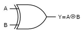
Fig.: XOR gate
It is similar to that of OR gate with an exception for few combination(s) of inputs. Hence, the output is also known as an odd function.
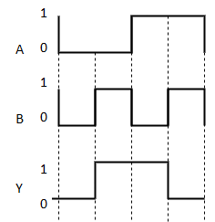
Timing Diagram:
Ex-NOR gate
It stands for Exclusive-NOR gate. Its function is same as that of NOR gate except when the inputs having even number of ones.
The truth table of 2-input Ex-NOR gate is:
A | B | Y = A⊙B |
0 | 0 | 1 |
0 | 1 | 0 |
1 | 0 | 0 |
1 | 1 | 1 |
Here A, B are the inputs and Y is the output. It is same as Ex-NOR gate with the only modification in the fourth row. The output is 1 instead of 0, when both the inputs are one.
Hence the output of Ex-NOR gate is ‘1’, when both inputs are same and 0, when both the inputs are different.
The symbol of Ex-NOR gate is:

Fig.: XNOR gate
It is similar to NOR gate except for few combination(s) of inputs. Here the output is ‘1’, when even number of 1 is present at the inputs. Hence is also called as an even function.
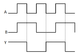
Timing Diagram:

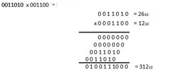
Q3) Multiply 0011010 001100
A3)

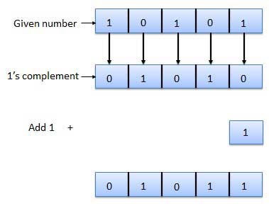
Q4) Find 2’s complement for 10101.
A4)

Q5) Convert (11101)2 to BCD.
A5)
Step 1 − Convert to Decimal
Binary Number − 111012
Its Decimal Equivalent −
Step | Binary Number | Decimal Number |
Step 1 | 111002 | ((1 × 24) + (1 × 23) + (1 × 22) + (0 × 21) + (0 × 20))10 |
Step 2 | 111002 | (16 + 8 + 4 + 0 + 0)10 |
Step 3 | 111002 | 2810 |
Binary Number − 111002 = Decimal Number − 2810
Step 2 -- Convert to BCD
Decimal Number − 2810
Its BCD Equivalent:
Step | Decimal Number | Conversion |
Step 1 | 2810 | 00102 10002 |
Step 2 | 2810 | 00101000BCD |
Result
(11100)2 = (00101000)BCD
Q6) Convert (1000)BCD to Excess-3.
A6)
Step 1 − Convert to decimal
(1000)BCD = 810
Step 2 − Add 3 to decimal
(8)10 + (3)10 = (11)10
Step 3 − Convert to Excess-3
(11)10 = (1011)2
Result
(1000)BCD = (1011)XS-3
Q7) Explain TTL.
A7)
1) Transistor-transistor logic (TTL) is a class of integrated circuits that maintains logic states and switches with the help of bipolar transistors.
2) It inputs rise to the logic "1" if left unconnected. It is one of the reasons that integrated circuits are widely used, as they are cheap, reliable and faster than RTL and DTL.
3) TTL makes use of transistors with multiple emitters in gates having multiple inputs.
4) The family of TTL is as follows:
- Standard TTL
It is used for 3.3-volt power supplies and memory interfacing.
- Fast TTL
It has faster switching than (6ns) but significantly higher power dissipation (22 mW).
- Schottky TTL
It uses Schottky diode clamps at gate inputs to prevent charge storage and improve switching time.
- Low power Schottky TTL
It is used for high resistance values of low-power TTL and the Schottky diodes provide a good combination of speed (9.5ns) and reduce power consumption (2 mW) too.
- Low power TTL
It is traded switching speed (33ns) for a reduction in power consumption (1 mW).
- Advanced Schottky TTL
It speeds up the low-to-high transition of TTL.
Advantages
- It is relatively easy in interfacing different circuits and produce complex logic functions.
- It has good noise margins as well as guaranteed voltage levels.
- It has good fan-in and is largely immune to damage from static electricity discharges
Disadvantages
- It has limited speed, low frequency, very noisy, high power consumption at higher frequencies.

Fig. TTL
Q8) Explain CMOS.
A8)
1) The MOSFET (metal-oxide-semiconductor field-effect transistor) are of two types : PMOS (p-type MOS) and NMOS (n-type MOS).
2) A new type of MOSFET logic is made combining both the PMOS and NMOS processes and is called as complementary MOS (CMOS).
3) CMOS stands for “Complementary Metal Oxide Semiconductor”.
4) It is one of the most popular technology in the chip design industry and is used today to form integrated circuits or various applications.
5) Computer memories, CPUs and cell phones make use of this technology due to various advantages. This technology uses both P and N channel semiconductor devices.
CMOS Applications
- Computer memories, CPUs
- Microprocessor designs
- Flash memory chip designing
- Used to design application specific integrated circuits (ASICs)
Advantages
- The power dissipation is very small.
- Greater number of IC’s can be integrated on a single chip.

Fig. CMOS
Q9) What are alpha numeric codes? Explain.
A9)
A binary digit or bit can be represented by two symbols as '0' or '1'.
This is not sufficient for communication between two computers as we need many more symbols for communication.
These symbols are representing 26 alphabetic characters with capital and small letters, numbers from 0 to 9, punctuation marks and other symbols.
These alphanumeric codes represent numbers and alphabetic characters.
Most of them also represent other characters like symbol and various instructions necessary for conveying information.
The code at least represents 10 digits and 26 letters of alphabet i.e. total 36 items.
The following three types of alphanumeric codes are commonly used for the data representation.
- American Standard Code for Information Interchange (ASCII).
- Extended Binary Coded Decimal Interchange Code (EBCDIC).
- Five bit Baudot Code.
Unit - 1
Unit - 1
Unit - 1
Binary Codes and Boolean algebra
Q1) Explain universal gates in detail.
A1)
NAND gate
It is a digital circuit which has two or more inputs and single output and it is the inversion of logical AND gate.
The truth table of 2-input NAND gate is:
A | B | Y = (A.B)’ |
0 | 0 | 1 |
0 | 1 | 1 |
1 | 0 | 1 |
1 | 1 | 0 |
Here A, B are the inputs and Y is the output of two input NAND gate. When both inputs are ‘1’, then the output, Y is ‘0’. If at least one of the input is zero, then the output, Y is ‘1’. This is just the inverse of AND operation.
The image shows the symbol of NAND gate:

Fig.: NAND gate
NAND gate works same as AND gate followed by an inverter.
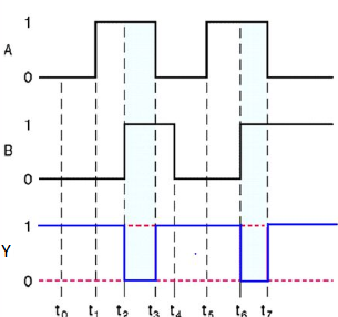
Timing Diagram:
NOR gate
It is a digital circuit that has two or more inputs and a single output which is the inversion of logical OR of all inputs.
The truth table of 2-input NOR gate is:
A | B | Y = (A+B)’ |
0 | 0 | 1 |
0 | 1 | 0 |
1 | 0 | 0 |
1 | 1 | 0 |
Here A and B are the two inputs and Y is the output. If both inputs are ‘0’, then the output is ‘1’. If any one of the input is ‘1’, then the output is ‘0’. This is exactly opposite to two input OR gate operation.
The symbol of NOR gate is:

Fig.: NOR gate
NOR gate works exactly same as that of OR gate followed by an inverter.
Timing Diagram:

Q2) Explain EX-OR gate and Ex-NOR gate.
A2)
Ex-OR gate
It stands for Exclusive-OR gate. Its function varies when the inputs have even number of ones.
The truth table of 2-input Ex-OR gate is:
A | B | Y = A⊕B |
0 | 0 | 0 |
0 | 1 | 1 |
1 | 0 | 1 |
1 | 1 | 0 |
Here A, B are the inputs and Y is the output of two input Ex-OR gate. The output (Y) is zero instead of one when both the inputs are one.
Therefore, the output of Ex-OR gate is ‘1’, when only one of the two inputs is ‘1’. And it is zero, when both inputs are same.
The symbol of Ex-OR gate is as follows:

Fig.: XOR gate
It is similar to that of OR gate with an exception for few combination(s) of inputs. Hence, the output is also known as an odd function.
Timing Diagram:

Ex-NOR gate
It stands for Exclusive-NOR gate. Its function is same as that of NOR gate except when the inputs having even number of ones.
The truth table of 2-input Ex-NOR gate is:
A | B | Y = A⊙B |
0 | 0 | 1 |
0 | 1 | 0 |
1 | 0 | 0 |
1 | 1 | 1 |
Here A, B are the inputs and Y is the output. It is same as Ex-NOR gate with the only modification in the fourth row. The output is 1 instead of 0, when both the inputs are one.
Hence the output of Ex-NOR gate is ‘1’, when both inputs are same and 0, when both the inputs are different.
The symbol of Ex-NOR gate is:
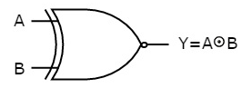
Fig.: XNOR gate
It is similar to NOR gate except for few combination(s) of inputs. Here the output is ‘1’, when even number of 1 is present at the inputs. Hence is also called as an even function.
Timing Diagram:
Q3) Multiply 0011010 001100
A3)
Q4) Find 2’s complement for 10101.
A4)
Q5) Convert (11101)2 to BCD.
A5)
Step 1 − Convert to Decimal
Binary Number − 111012
Its Decimal Equivalent −
Step | Binary Number | Decimal Number |
Step 1 | 111002 | ((1 × 24) + (1 × 23) + (1 × 22) + (0 × 21) + (0 × 20))10 |
Step 2 | 111002 | (16 + 8 + 4 + 0 + 0)10 |
Step 3 | 111002 | 2810 |
Binary Number − 111002 = Decimal Number − 2810
Step 2 -- Convert to BCD
Decimal Number − 2810
Its BCD Equivalent:
Step | Decimal Number | Conversion |
Step 1 | 2810 | 00102 10002 |
Step 2 | 2810 | 00101000BCD |
Result
(11100)2 = (00101000)BCD
Q6) Convert (1000)BCD to Excess-3.
A6)
Step 1 − Convert to decimal
(1000)BCD = 810
Step 2 − Add 3 to decimal
(8)10 + (3)10 = (11)10
Step 3 − Convert to Excess-3
(11)10 = (1011)2
Result
(1000)BCD = (1011)XS-3
Q7) Explain TTL.
A7)
1) Transistor-transistor logic (TTL) is a class of integrated circuits that maintains logic states and switches with the help of bipolar transistors.
2) It inputs rise to the logic "1" if left unconnected. It is one of the reasons that integrated circuits are widely used, as they are cheap, reliable and faster than RTL and DTL.
3) TTL makes use of transistors with multiple emitters in gates having multiple inputs.
4) The family of TTL is as follows:
- Standard TTL
It is used for 3.3-volt power supplies and memory interfacing.
- Fast TTL
It has faster switching than (6ns) but significantly higher power dissipation (22 mW).
- Schottky TTL
It uses Schottky diode clamps at gate inputs to prevent charge storage and improve switching time.
- Low power Schottky TTL
It is used for high resistance values of low-power TTL and the Schottky diodes provide a good combination of speed (9.5ns) and reduce power consumption (2 mW) too.
- Low power TTL
It is traded switching speed (33ns) for a reduction in power consumption (1 mW).
- Advanced Schottky TTL
It speeds up the low-to-high transition of TTL.
Advantages
- It is relatively easy in interfacing different circuits and produce complex logic functions.
- It has good noise margins as well as guaranteed voltage levels.
- It has good fan-in and is largely immune to damage from static electricity discharges
Disadvantages
- It has limited speed, low frequency, very noisy, high power consumption at higher frequencies.
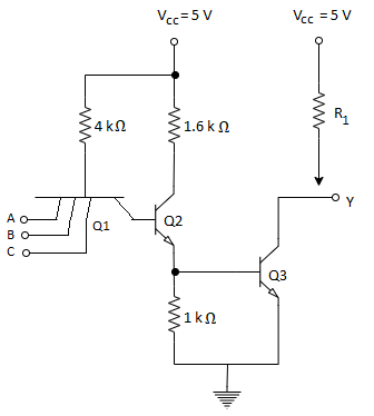
Fig. TTL
Q8) Explain CMOS.
A8)
1) The MOSFET (metal-oxide-semiconductor field-effect transistor) are of two types : PMOS (p-type MOS) and NMOS (n-type MOS).
2) A new type of MOSFET logic is made combining both the PMOS and NMOS processes and is called as complementary MOS (CMOS).
3) CMOS stands for “Complementary Metal Oxide Semiconductor”.
4) It is one of the most popular technology in the chip design industry and is used today to form integrated circuits or various applications.
5) Computer memories, CPUs and cell phones make use of this technology due to various advantages. This technology uses both P and N channel semiconductor devices.
CMOS Applications
- Computer memories, CPUs
- Microprocessor designs
- Flash memory chip designing
- Used to design application specific integrated circuits (ASICs)
Advantages
- The power dissipation is very small.
- Greater number of IC’s can be integrated on a single chip.
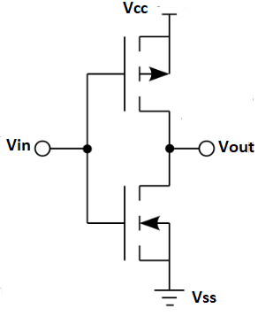
Fig. CMOS
Q9) What are alpha numeric codes? Explain.
A9)
A binary digit or bit can be represented by two symbols as '0' or '1'.
This is not sufficient for communication between two computers as we need many more symbols for communication.
These symbols are representing 26 alphabetic characters with capital and small letters, numbers from 0 to 9, punctuation marks and other symbols.
These alphanumeric codes represent numbers and alphabetic characters.
Most of them also represent other characters like symbol and various instructions necessary for conveying information.
The code at least represents 10 digits and 26 letters of alphabet i.e. total 36 items.
The following three types of alphanumeric codes are commonly used for the data representation.
- American Standard Code for Information Interchange (ASCII).
- Extended Binary Coded Decimal Interchange Code (EBCDIC).
- Five bit Baudot Code.