Unit - 1
Introduction
Q1) Draw and explain block diagram of digital communication.
A1)
The elements which form a digital communication system is represented by the following block diagram for the ease of understanding.
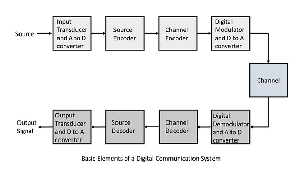
Following are the sections of the digital communication system.
Source
The source can be an analog signal.
Example: A Sound signal
Input Transducer
This is a transducer which takes a physical input and converts it to an electrical signal. This block also consists of an analog to digital converter where a digital signal is needed for further processes.
A digital signal is generally represented by a binary sequence.
Source Encoder
The source encoder compresses the data into minimum number of bits. This process helps in effective utilization of the bandwidth. It removes the redundant bits unnecessary excess bits, i.e. ,zeroes.
Channel Encoder
The channel encoder, does the coding for error correction. During the transmission of the signal, due to the noise in the channel, the signal may get altered and hence to avoid this, the channel encoder adds some redundant bits to the transmitted data. These are the error correcting bits.
Digital Modulator
The signal to be transmitted is modulated here by a carrier. The signal is also converted to analog from the digital sequence, in order to make it travel through the channel or medium.
Channel
The channel or a medium, allows the analog signal to transmit from the transmitter end to the receiver end.
Digital Demodulator
This is the first step at the receiver end. The received signal is demodulated as well as converted again from analog to digital. The signal gets reconstructed here.
Channel Decoder
The channel decoder, after detecting the sequence, does some error corrections. The distortions which might occur during the transmission, are corrected by adding some redundant bits. This addition of bits helps in the complete recovery of the original signal.
Source Decoder
The resultant signal is once again digitized by sampling and quantizing so that the pure digital output is obtained without the loss of information. The source decoder recreates the source output.
Output Transducer
This is the last block which converts the signal into the original physical form, which was at the input of the transmitter. It converts the electrical signal into physical output.
Output Signal
This is the output which is produced after the whole process.
Q2) Compare analog and digital communication.
A2)
PARAMETERS | ANALOG COMMUNICATION | DIGITAL COMMUNICATION |
Definition | Analog Communication is the technology which uses Analog signal for the transmission of information. | Digital Communication is the technology which uses digital signal for the transmission of information. |
Noise and Distortion | Get affected by Noise | Immune from Noise and Distortion |
Error Probability | Error Probability is high due to parallax. | Error Probability is low |
Hardware | Hardware is complicated and less flexible than digital system. | Hardware is flexible and less complicated than Analog system. |
Cost | Low Cost | High Cost |
Bandwidth Requirement | Low bandwidth requirement | High bandwidth Requirement |
Power Requirement | High power is required | Low Power Requirement |
Portability | Less Portable as the components are heavy | More portable due to compact equipments. |
Modulation Used | Amplitude and Angle Modulation | Pulse coded Modulation or PCM, DPCM etc. |
Representation of Signal | Analog signal can be represented by sine wave. | Digital signal is represented by square wave. |
Signal Values | Consists of continuous values | Consists of discrete values |
Example of Signal | Analog signal comprises of voice, sound etc. | Digital signals are used in computers |
Q3) State and explain sampling theorem.
A3)
The sampling theorem, which is also called as Nyquist theorem, delivers the theory of sufficient sample rate in terms of bandwidth for the class of functions that are bandlimited.
The sampling theorem states that, “a signal can be exactly reproduced if it is sampled at the rate fs which is greater than twice the maximum frequency W.”
Let us consider a band-limited signal, i.e., a signal whose value is non-zero between some –W and W Hertz.
Such a signal is represented as x(f)=0 for ∣f∣>W
For the continuous-time signal x (t), the band-limited signal in frequency domain, can be represented as shown in the following figure.
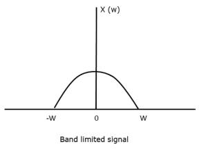
If the signal x(t) is sampled above the Nyquist rate, the original signal can be recovered, and if it is sampled below the Nyquist rate, the signal cannot be recovered.
The following figure explains a signal, if sampled at a higher rate than 2w in the frequency domain.
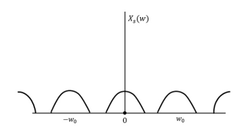
The above figure shows the Fourier transform of a signal xs (t).
If fs<2W
The resultant pattern will look like the following figure.
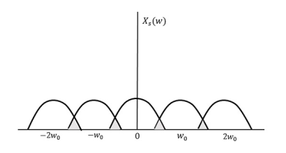
Here, the over-lapping of information is done, which leads to mixing up and loss of information. This unwanted phenomenon of over-lapping is called as Aliasing.
Q4) Draw and explain basic elements of PCM.
A4)
The transmitter section comprises of Sampling, Quantizing and Encoding. The low pass filter prior to sampling prevents aliasing of the message signal.
The basic operations in the receiver section are regeneration of impaired signals, decoding, and reconstruction of the quantized pulse train.
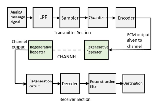
Low Pass Filter
This filter eliminates the high frequency components present in the input analog signal to avoid aliasing of the message signal.
Sampler
It helps to collect the sample data at instantaneous values of message signal, so as to reconstruct the original signal. The sampling rate must be in accordance with the sampling theorem.
Quantizer
It reduces excessive bits and confines the data. It reduces the redundant bits and compresses the value of the sampled output.
Encoder
The digitization of analog signal is done by the encoder. It designates each quantized level by a binary code. Encoding minimizes the bandwidth used.
Regenerative Repeater
It increases the signal strength. The output of the channel also has one regenerative repeater circuit, to compensate the signal loss and reconstruct the signal, and also to increase its strength.
Decoder
The decoder circuit decodes the pulse coded waveform to reproduce the original signal. This circuit acts as the demodulator.
Reconstruction Filter
After the digital-to-analog conversion is done by the regenerative circuit and the decoder, a low-pass filter is employed, called as the reconstruction filter to get back the original signal.
Hence, the Pulse Code Modulator circuit digitizes the given analog signal, codes it and samples it, and then transmits it in an analog form. This whole process is repeated in a reverse pattern to obtain the original signal.
Q5) Explain adaptive delta modulation.
A5)
In digital modulation, we have come across certain problem of determining the step-size, which influences the quality of the output wave.
A larger step-size is needed in the steep slope of modulating signal and a smaller step size is needed where the message has a small slope. The minute details get missed in the process. So, it would be better if we can control the adjustment of step-size, according to our requirement in order to obtain the sampling in a desired fashion. This is the concept of Adaptive Delta Modulation.
Following is the block diagram of Adaptive delta modulator.
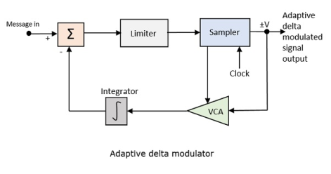
The gain of the voltage controlled amplifier is adjusted by the output signal from the sampler. The amplifier gain determines the step-size and both are proportional.
ADM quantizes the difference between the value of the current sample and the predicted value of the next sample. It uses a variable step height to predict the next values, for the faithful reproduction of the fast varying values.
Q6) Explain delta sigma modulation.
A6)
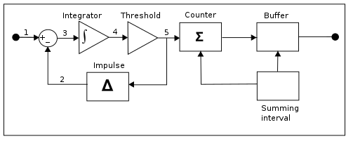
- Delta-sigma (ΔΣ; or sigma-delta, ΣΔ) modulation is a method for encoding analog signals into digital signals as found in an analog-to-digital converter (ADC).
- It is used to convert high bit-count, low-frequency digital signals into lower bit-count, higher-frequency digital signals as part of the process to convert digital signals into analog as part of a digital-to-analog converter (DAC).
- In this, accuracy of the modulation is improved by passing the digital output through a 1-bit DAC and adding (sigma) the resulting analog signal to the input signal, thereby reducing the error introduced by the delta modulation.
- Both ADCs and DACs can employ delta-sigma modulation.
- A delta-sigma ADC first encodes an analog signal using high-frequency delta-sigma modulation, and then applies a digital filter to form a higher-resolution but lower sample-frequency digital output.
- A delta-sigma DAC encodes a high-resolution digital input signal into a lower-resolution but higher sample-frequency signal that is mapped to voltages, and then smoothed with an analog filter.
- In both cases, the temporary use of a lower-resolution signal simplifies circuit design and improves efficiency.
- Primarily because of its cost efficiency and reduced circuit complexity, it is used in modern electronic components such as DACs, ADCs, frequency synthesizers, switched-mode power supplies and motor controllers.
Q7) Explain DPCM in detail.
A7)
DPCM Transmitter
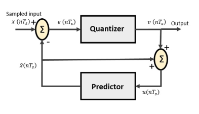
The DPCM Transmitter consists of Quantizer and Predictor with two summer circuits.
Following is the block diagram of DPCM transmitter.
The signals at each point are named as −
- x(nTs) is the sampled input
- xˆ(nTs) is the predicted sample
- e(nTs) is the difference of sampled input and predicted output, often called as prediction error
- v(nTs) is the quantized output
- u(nTs) is the predictor input which is actually the summer output of the predictor output and the quantizer output
The predictor produces the assumed samples from the previous outputs of the transmitter circuit. The input to this predictor is the quantized versions of the input signal x(nTs).
Quantizer Output is represented as −
v(nTs)=Q[e(nTs)]
=e(nTs)+q(nTs)
Where q (nTs) is the quantization error
Predictor input is the sum of quantizer output and predictor output,
u(nTs)= +v(nTs)
u(nTs)= +e(nTs)+q(nTs)
u(nTs)=x(nTs)+q(nTs)
The same predictor circuit is used in the decoder to reconstruct the original input.
DPCM Receiver
The block diagram of DPCM Receiver consists of a decoder, a predictor, and a summer circuit. Following is the diagram of DPCM Receiver.
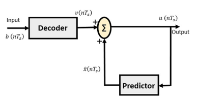
The notation of the signals is the same as the previous ones. In the absence of noise, the encoded receiver input will be the same as the encoded transmitter output.
As mentioned before, the predictor assumes a value, based on the previous outputs. The input given to the decoder is processed and that output is summed up with the output of the predictor, to obtain a better output.
Q8) What is companding? Explain various techniques.
A8)
It is a combination of Compressing and Expanding, which means that it does both. This is a non-linear technique used in PCM which compresses the data at the transmitter and expands the same data at the receiver. The effects of noise and crosstalk are reduced by using this technique.
There are two types of Companding techniques. They are −
A-law Companding Technique
- Uniform quantization is achieved at A = 1, where the characteristic curve is linear and no compression is done.
- A-law has mid-rise at the origin. Hence, it contains a non-zero value.
- A-law companding is used for PCM telephone systems.
µ-law Companding Technique
- Uniform quantization is achieved at µ = 0, where the characteristic curve is linear and no compression is done.
- µ-law has mid-tread at the origin. Hence, it contains a zero value.
- µ-law companding is used for speech and music signals.
µ-law is used in North America and Japan.
Q9) Define aliasing.
A9)
Aliasing can be referred to as “the phenomenon of a high-frequency component in the spectrum of a signal, taking on the identity of a low-frequency component in the spectrum of its sampled version.”