Unit – 3
8051 serial Communication
Q1) Explain the interrupt structure of 8051?
A1) An interrupt is an event that occurs randomly in the flow of continuity. 8051 architecture handles 5 interrupt sources,
- Two are internal that is the Timer Interrupts
- Two are external and
- A serial interrupt.

Interrupt structure
Q2) Explain the SFR associated with interrupt structure?
A2)
Interrupt Enable (IE)Register
This register can be used to enable or disable interrupts programmatically. This register is an SFR. The address is A8H. This byte is bit addressable. So it can be programmed by the user.
Bit Address | AF
| AE | AD | AC | AB | AA | A9 | A8 |
Bit Details | EA | X | X | ES | ET1 | EX1 | ET0 | EX0 |
IE Register
Bit Details | High Value(1) | Low Value(0) |
EA | Least significant 5 bits can decide enable or disable these five interrupts | Disable all five interrupts . It just ignores the rest five bits |
ES | Enable Serial Port Interrupt | Disable Serial Port Interrupt |
ET1 | Enable Timer1 Interrupt | Disable Timer1 Interrupt |
EX1 | Enable external interrupt1 | Disable external interrupt1 |
ET0 | Enable Timer0 interrupt | Disable Timer0 Interrupt |
EX0 | Enable external interrupt 0 | Disable external interrupt 0 |
External Interrupt
The external interrupts of 8051 are INT0and. INT1 These interrupts can be programmed to either edge-triggered or level triggered. The TCON register can be used top rogram external interrupts to edge or level triggered. The TCON isTimer Control. TCON is another bit addressable SFR. Here the address is 88H.
Bit Address | 8F | 8E | 8D | 8C | 8B | 8A | 89 | 88 |
Bit Details | TF1 | TR1 | TF0 | TR0 | IE1 | IT1 | IE0 | IT0 |
Bit Details | High Value(1) | Low Value(0) |
IT0 | Set INT0 as negative edge triggered input | Set INT0 as active low level triggered input. |
IT1 | Set INT1 as negative edge triggered input | Set INT1 as active low level triggered input. |
IE0 | This will be 1. When INT0 is activated as level triggered | This will be 0 when INT0 is activated as edge triggered |
IE1 | This will be 1. When INT1 is activated as level triggered | This will be 0 when INT1 is activated as edge triggered |
TR0 | Set Timer0 as run mode | Set Timer0 as stop mode. |
TR1 | Set Timer1 as run mode | Set Timer1 as stop mode |
TF0 | High when Timer0 overflow occurs | After resetting the timer 0 this will also be changed to 0 state |
TF1 | High when Timer1 overflow occurs | After resetting the timer T1 this will also be changed to 0 state |
Serial Port Interrupt
The serial ports can be used either Transmitting mode or reception mode. The interrupt status for the Transmission is provided by TI, and status for Reception is provided by RI. These are two bits of SCON(Serial Control). This is also a bit addressable SFR. The address is98H
Bit Address | 9F | 9E | 9D | 9C | 9B | 9A | 99 | 98 | ||
Bit Details | SM0 | SM1 | SM2 | REN | TB8 | RB8 | TI | RI | ||
Bit Details | Description | |||||||||
SM0 | This is Serial Port Mode0 shift register | |||||||||
SM1 | This is Serial Port Mode 1 (8-bit UAR + variable) | |||||||||
SM2 | Enable multiprocessor communication in the mode 2 or 3 | |||||||||
REN | Set or reset by the software to enable or disable the Reception | |||||||||
TB8 | It indicates the 9th bit that will be transmitted in mode 2 or 3. It can be set or reset by software | |||||||||
RB8 | In mode 2 or 3 the 9th bit was received in mode 1. | |||||||||
TI | The transmission interrupt flag . It can be set by hardware | |||||||||
RI | The receiver interrupt flag . It can be set by hardware | |||||||||
Q3) Explain the Programming External Hardware Interrupts in C?
A3)
The external interrupts are the interrupts received from the (external) devices interfaced with the microcontroller. They are received at INTx pins of the controller.
These can be level triggered or edge triggered.
In level triggered, interrupt is enabled for a low at INTx pin; while in case of edge triggering, interrupt is enabled for a high to low transition at INTx pin. The edge or level trigger is decided by the TCON register.
The TCON register has following bits:
TCON:

Setting the IT0 and IT1 bits make the external interrupt 0 and 1 edge triggered respectively. By default these bits are cleared and so external interrupt is level triggered.
Following are the steps for using external interrupt:
1. Enable external interrupt by configuring IE register.
2. Write routine for external interrupt. The interrupt number is 0 for EX0 and 2 for EX1 respectively.
Q4) What are the two types of external interrupts?
A4)
//Level trigger external interrupt
Void main()
{
IE = 0x81;
While(1);
}
Void ISR_ex0(void) interrupt 0
{
<body of interrupt>
}
Example code
//Edge trigger external interrupt
Void main()
{
IE = 0x84;
IT1 = 1;
While(1);
}
Void ISR_ex1(void) interrupt 2
{
<body of interrupt>
}
Q5) What is ADC?
A5)
ADC0808/0809 is a monolithic CMOS device which has 28 pin and gives 8-bit value in output and 8- channel ADC input pins (IN0-IN7). I
It has resolution of 8 so it can encode the analog data into one of the 256 levels (28).
This device has three channel address line namely: ADDA, ADDB and ADDC for selecting channel.
Q6) Explain Pin diagram of ADC0808?
A6)

ADC 0808 Pin
ADC0808/0809 requires a clock pulse for conversion. This can be provided by using oscillator or by using microcontroller.
Select the input channel using address lines, like the input line IN0 by keeping all three address lines (ADDA, ADDB,ADDC) low.
Suppose IN2 is selected the keep ADDA and ADDB low and ADDC high.
ADC Channel name | ADDC Pin | ADDB Pin | ADDA Pin |
IN0 | Low | Low | Low |
IN1 | Low | Low | High |
IN2 | Low | High | Low |
IN3 | Low | High | High |
IN4 | High | Low | Low |
IN5 | High | Low | High |
IN6 | High | High | Low |
IN7 | High | High | High |
Q7) Explain the interfacing of ADC with 8051?
A7)
First the microcontroller provides a 500 KHz clock signal to ADC0808 because the Timer 0 interrupt as ADC requires clock signal to operate.
Then the microcontroller sends a LOW to HIGH level signal to ALE pin (active-high pin) of ADC0808 to enable the latch in the address.
By applying HIGH to LOW Level signal to SC (Start Conversion), ADC starts analog to digital conversion. And then wait for the EOC (End of Conversion) pin to go LOW.
When EOC goes LOW, it means analog to digital conversion has been completed and data is ready to use.
After this, microcontroller enables the output line by applying a HIGH to LOW signal to OE pin of ADC0808.
ADC0808 gives ratio metric conversion output at its output pins.
Radiometric conversion is given by
Vin/(Vfs – Vz) = Dx / (Dmax – Dmin)
Where:
Vin is input voltage for conversion
Vfs is full scale voltage
Vz is zero voltage
Dx is data point being measured
Dmax is maximum data limit
Dmin is minimum data limit.
Interfacing Diagram:

Interfacing 8051 with ADC0808
Q8) Explain the program for interfacing 8051 with ADC?
A8)
SOC EQU P2.6
EOC EQU P2.5
OE EQU P2.4
ALE EQU P2.3
ADDR_C EQU P2.2
ADDR_B EQU P2.1
ADDR_A EQU P2.0
ORG 0000H
MOV P1, #0FFH
SETB P2.5
CLR SOC
CLR OE
CLR ALE
AGAIN: CLR ADDR_C
CLR ADDR_B
CLR ADDR_A
SETB SOC
SET ALE
ACALL DELAY
CLR SOC
CLR ALE
BACK: JB EOC BACK
HERE: JNB EOC HERE
SETB OE
MOV A,P1
ACALL CONVERSION
ACALL DISPLAY
AGAIN: SJMP AGAIN
Q9) What is SOC and EOC?
A9)
SOC [Start of conversion]:
When High to low signal is appears to this pin of ADC, ADC then starts conversion

SOC
EOC [End of conversion]:
ADC sends this high EOC signal to Micro-Controller to indicate completion of conversion.
Q10) Explain output enable?
A10)
When a high signal is applied to this pin, the output latch of ADC get enables and the converted data is then available to Micro-Controller.
The reference voltage determines the range of analog input voltage.
For example: - If reference voltage is 5V then analog voltage range is from 0V-5V. If the reference voltage is 2.56V then the Analog signal range is from 0V-2.56V.
The frequency of clock signal applied determines the conversion speed.
Q11) Explain TMOD register.
A11)
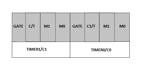
TMOD is an 8-bit register for selecting timer or counter and mode of timers. The lower 4-bits are used for control operation of timer 0 or counter0. The remaining 4-bits for control operation of timer1 or counter1.This register is present in SFR register and the address for SFR register is 89th.

Timer Mode Control
Gate: If the gate bit is set to ‘0’, then we can start and stop the “software” timer in the same way. If the gate is set to ‘1’, then we can perform hardware timer.
C/T: If the C/T bit is ‘1’, then it is acting as a counter mode, and similarly when set C+
=/T bit is ‘0’; it is acting as a timer mode.
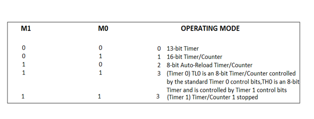
Mode select bits: The M1 and M0 are mode select bits, which are used to select the timer operations. There are four modes to operate the timers.
Mode 0: This is a 13-bit mode that means the timer operation completes with “8192” pulses.
Mode 1: This is a16-bit mode, which means the timer operation completes with maximum clock pulses that “65535”.
Mode 2: This mode is an 8-bit auto reload mode, which means the timer operation completes with only “256” clock pulses.
Mode 3: This mode is a split-timer mode, which means the loading values in T0 and automatically starts the T1.

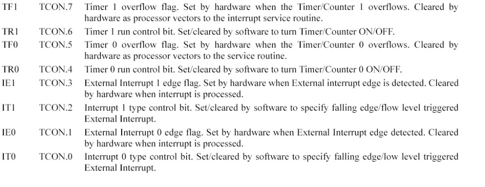
Q12) Explain TCON register.
A12)


Q13) Program to transfer letter “D” serially at 9800baud, continuously
A13)
MOV TMOD, #20H; timer 1, mode 2(auto reload)
MOV TH1, #-3; 9600 baud rate
MOV SCON, #50H; 8-bit, 1 stop,
REN enabled
SETB TR1; start timer 1
AGAIN: MOV SBUF, #”D”; letter “D” to transfer
HERE: JNB TI, HERE; wait for the last bit
CLR TI; clear TI for next char
SJMP AGAIN; keep sending A
Steps to receive data serially:
1. Set baud rate by loading TMOD register with the value 20H, this indicating timer 1 in mode 2 (8-bit auto-reload) to set baud rate
2. The TH1 is loaded with proper values to set baud rate
3. The SCON register is loaded with the value 50H, indicating serial mode 1, where an 8- bit data is framed with start and stop bits
4. TR1 is set to 1 to start timer 1
5. RI is cleared by CLR RI instruction
6. The RI flag bit is monitored with the use of instruction JNB RI, xx to see if an entire character has been received yet
7. When RI is raised, SBUF has the byte; its contents are moved into a safe place
8. To receive next character, go to step 5
Q14) Program to receive bytes of data serially, and put them in P2, set the baud rate at 9600, 8-bit data, and 1 stop bit.
A14)
MOV TMOD, #20H; timer 1, mode 2(auto reload)
MOV TH1, #-3; 9600 baud rate MOV SCON, #50H; 8-bit, 1 stop,
REN enabled SETB TR1; start timer 1
HERE: JNB RI, HERE; wait for char to come in
MOV A, SBUF; saving incoming byte in A
MOV P2, A; send to port 1
CLR RI; get ready to receive next byte
SJMP HERE; keep getting data