Unit - 5
Basic concept of PIC microcontroller
Q1) Compare microprocessor and microcontroller?
A1)
| Microprocessor | Microcontroller |
System | It is the heart of the computer system, | It is the heart of an embedded system. |
Contains | It contains CPU, general purpose registers, stack pointers, program counters, clock timing and interrupt circuits. | It contains the circuitry of microprocessor and has built-in ROM, RAM, I/O devices, timers and counters. |
Data memory | It has many instructions to move data between memory and CPU | It has one or two instructions to move data between memory and CPU. |
Circuit | It is large | It is small |
Cost | Cost of the entire system increases | Cost of the entire system is low. |
Bit instructions | It has one- or two-bit handling instructions. | It has many bit handling instructions |
Register numbers | It has less number of registers; hence the operations are memory based. | It has more number of registers; hence the programs are easier to write. |
Storage | It is based on Von Neumann architecture, where the program and data are stored in the same memory module. | It is based on the Harvard architecture, where the program memory and data memory are stored in separate module |
Time | Access time for memory and I/O devices is more. | Less access time for built-in memory and I/O devices. |
Hardware | It requires more hardware | It requires less hardware. |
Q2) List comparison between the PIC family?
A2)
PIC Family | No. Of Pins | Flash ROM | RAM | Timers | I/O Pins | ADC input channels | Additional features |
PIC10CXX | 6 | 896 Bytes | 64 Bytes | 2 | 4 | 2 Channels (8 -bit Digital Result) | PWM module |
PIC12CXX | 8 | 3.5 KB | 128-256 Bytes | 2 | 6 | 3 Channels (8 -bit Digital Result) | USART, PWM module |
PIC16FXX | 14-40 | 7 to 28 KB | 512 Bytes to 2 KB | 4 | 12 | 4 Channels (10 -bit Digital Result) | WDT, Data E, USART, 12C, SPI-EEPROM, PWM module |
PIC18FXX | 40-100 | 2 MB | 32 to 128 KB | 4 | 33-72 | 12 Channels (10 -bit Digital Result) | USB, 12-bit ADC, CAN, I2C, SPI Bus, USART, PWM module |
Q3) Compare the RISC and CISC processor?
A3)
No. | RISC | CISC |
1. | Simple instructions taking one cycle | Complex instructions taking multiple cycles |
2. | Very few instructions refer memory | Most of instructions may refer memory |
3. | Instructions are executed by hardware | Instructions are executed by microprogram |
4. | Fixed format instructions | Variable format instructions |
5. | Few instructions | Many instructions |
6. | Few addressing mode, and most instructions have register to register addressing mode | Many addressing modes |
7. | Complexed addressing modes are synthesized in software. | Supports complex addressing modes |
8. | Multiple register sets | Single register set |
9. | Highly pipelined | Not pipelined or less pipelined |
10. | Complexity is in the compiler | Complexity is in the microprogram |
11. | Conditional jump can be based on a bit anywhere in memory. | Conditional jump is usually based on status register bit. |
Q4) List all the features of PIC microcontroller?
A4)
- This has high performance RISC CPU.
- 40-pin PDIP, high performance, enhanced Flash Microcontroller with CAN.
- The Operating speed ranges between 40 MHz up to 10 MIPS.
- The Operating voltage ranges 4.2 to 5.5 V.
- ROM of size 2M bytes
- RAM between 256 bytes to 4096 bytes.
- On-chip program ROM in form of flash memory.
- Data EEPROM
- 8 x 8 Single cycle Hardware Multiplier
- 16-bit wide instructions, 8-bit wide data path.
- 75 instructions.
- ADC and USART PROTOCOL for PC communication.
- I/O port between 16 to 72 pins and I/O port register are bit and port accessible.
- SPI PROTOCOL and I2C PROTOCOL for memory communication.
- PIC 18F458 has two-stage pipeline.
- Interrupt capability with Priority levels.
- Linear program memory addressing upto 2 Mbytes
Q5) Write short note on MCU?
A5)
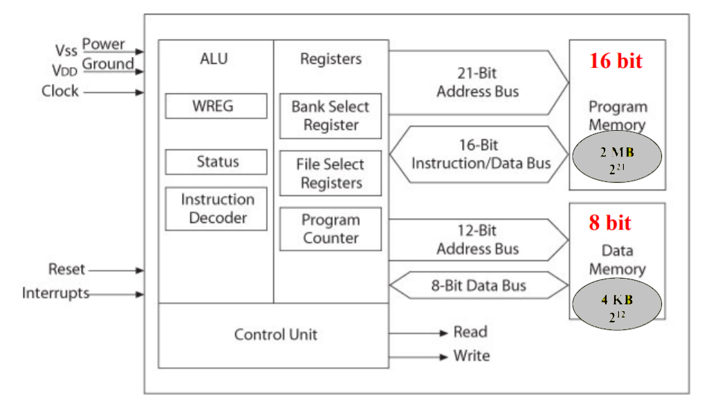
Fig. MCU and Memory
Includes Arithmetic Logic Unit (ALU), Registers, and Control Unit and Arithmetic Logic Unit (ALU)
- Performs logical and arithmetic functions
- WREG – working register (acts as an accumulator) – used to perform arithmetic or logical functions
- Status register that stores flags – indicates the status of the operation done by ALU
- Instruction decoder (ID)– when the instruction is fetched it goes into the ID to be interpreted – tell the processor what to do.
Registers – hold memory address
Bank Select Register (BSR)
4-bit register used in direct addressing the data memory.
File Select Registers (FSRs)
16-bit registers used as memory pointers in indirect addressing data memory n Program Counter (PC)
21-bit register that holds the program memory address while executing programs
Control unit- Provides timing and control signals to various Read and Write operations
Q6) Explain the data memory map of PIC 18 device?
A6)
Data Memory:
- PIC-18 has 4KB Data Memory.
- The data memory is divided into banks and each bank is 256 bytes.
- It consists of GPRs, SFRs referred as Data Registers.
- General purpose registers are used to hold dynamic data.
- SFRs are used to control the operation of Peripheral functions. Only one bank is active at a time.
- Access bank consists of lowest 96bytes and highest 160 bytes of data memory space.
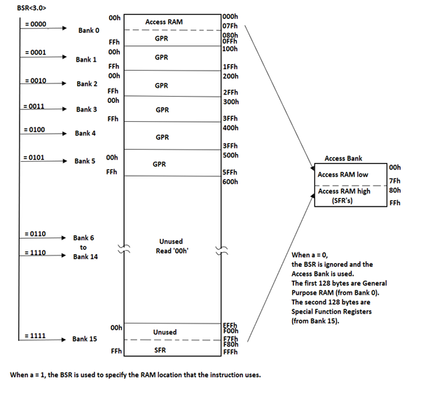
Figure. Data Memory map for PIC-18 Device.
Q7) Explain the program memory organisation of PIC-18?
A7)
Program Memory Organization:
- The program counter is 21-bit long which enables the user program to access up to 2MB program memory.
- After Power on it starts to execute the instruction from address 0
- The location 0x08 is reserved for high-priority ISR
- The location 0x18 is reserved for low-priority ISR.
- Upto 128KB of Program Memory is inside the MCU chip.
- Rest of the program memory is located outside the MCU chip.
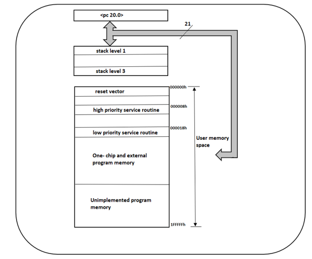
Figure. Program Memory Organization for PIC-18 device.
Q8) What are the banks of RAM explain in detail?
A8)
Four banks of Registers/RAM.
- The register/RAM in bank 0 at address between 0x000 and 0x07F
- The register/RAM in bank 1 at address between 0x080 and 0x0FF
- The register/RAM in bank 2 at address between 0x100 and 0x17F
- The register/RAM in bank 3 is at address between 0x180 and 0x1FF.
A byte at an address 0x25 accessed directly by using direct address 0x25 in the instruction. It is considered at bank 0 as 0x25 falls in bank 0 address space.
Direct Address
- A byte at an address 0x85 can be accessed by 7-bit direct address = 0x05 of Bank1
- Bank 1 base address is 0x80 and 0x85–0x80 = 0x05
Bank Pairs
- Four banks form two pairs of banks of Registers/RAM
- The register/RAM in lower bank pair is at address between 0x000 and 0x0FF
- A Bank pair needs 8-bit to access.
- The register/RAM in upper bank pair is at address between 0x100 and 0x1FF
- Bank-pair 0 address is 0x000 and 1 address is 0x100.
Register/RAM Bank Pair access
- By 8-bit address
- Bank pair is as per IRP bit
- 8-bit address is used when using indirect address for a register/RAM
- This address plus the bank-pair base address generates 9-bit address of a register/internal RAM
- Bank pair base address is as per IRP
RAM/File Register Select Register (FSR)
- FSR is used for indirect addressing in the instruction
- FSR of 8-bits
- It provides the 8-bit address of RAM/register in register file
- That address is in a bank-pair
- Bank pair is as per IRP bit in the STATUS.
IRP (indirect register-bank pair) bit
- Indirect address has 8-bits.
- These bits are taken from either lower pair of banks 0 or 1 or upper pair of banks 2 or 3
- Bit 7 in STATUS, when = 1, then upper bank-pair used
- When = 0 then lower bank pair used.
RP1-RP0 (register- pair higher bank register pair lower bank) bits
- Direct address has taken from 7-bits in the instruction
- They are taken for either bank 0 or 1 or 2 or 3.
- Bit 6-5 in STATUS, when = 11, then higher bank 3. When = 10, then bank 2. When = 01, then bank 1. When = 00, then bank 0.
Higher addresses Mirroring in all four banks
- Higher addresses 0x70-0x7F in a bank are also mirrored.
- When 0x70-0x7F is accessed, then it also means access to 0xF0H-0xFFH, 0x170-0x17F and 0x1F0-0x1FF.
- Frequently used variables are stored at these sixteen addresses by the programmer
Q9) Why we need reset operation in microcontrollers?
A9)
Reset keeps the microcontroller into known condition. For microcontroller to function properly it must be reset which means all the registers would be placed in starting position. It can be used to when trying out a device as interrupt in program execution.
For proper operation MCLR pin must be connected via resistor to positive supply. The resistor value varies between 5 and 10K. The function of the resistor is to keep certain line on logical one as preventive called as pull- up resistor.
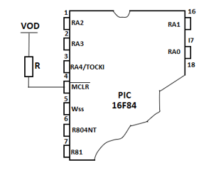
Figure. Reset
Q10) What are watch dog time. Explain its waveform and hardware too?
A10)
Watchdog timer is a hardware microcontroller. It is basically used to take out a system from an infinite loop and resets the system. Watchdog makes the embedded systems more reliable as it works as a safety mechanism.
Watchdog is a type of counter. It is an up counter which means that it counts from zero and reaches to some values. As soon the watchdog timer reaches some value its hardware generates a watchdog reset. Then the system resets this count value to zero in order to avoid system reset. The watchdog timer is loaded with some values which are based on its timeout time. The system needs to reset the counter before timeout.
Watchdog Timer Hardware
The figure below is of watchdog time hardware with input as clock. With every clock the internal counter increments. Then the comparator will compare this value with the loaded count value. Then if the comparator finds that count value matches the watchdog hardware generates and resets it.
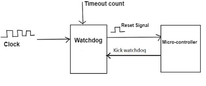
Fig. Watch dog timer
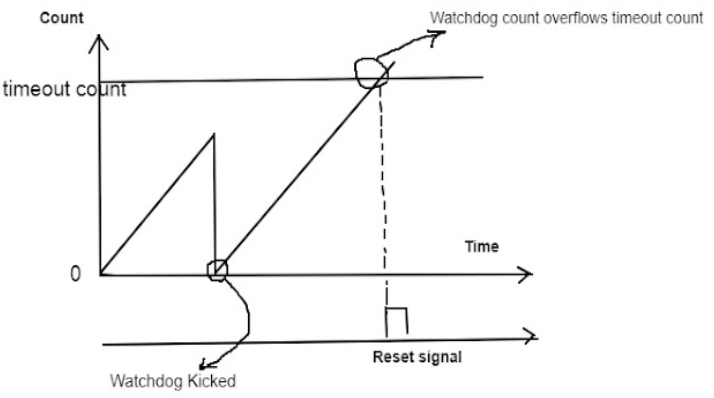
Fig. Timing Diagram
Watchdog in Microcontroller
The internal watchdog of the MSP430 family is used either as a simple timer or as a watchdog that ensures system integrity. The watchdog function is enabled after power-on reset or system reset. In case of any difficulties after start-up of MSP430, the watchdog will reset the system as often as it is needed for it to start successfully.
A system running with MCLK = 3 MHz uses the watchdog for supervision of three functions.
Power Fail — by checking the 60 Hz AC line.
Function 1 — A check is made if the software reaches this background part regularly
Function 3 — A check is made if this interrupt handler is called regularly.
Each supervised function sets a dedicated bit in RAM byte WDB in intervals less than 10.66 ms (power-up value of the watchdog with MCLK = 3 MHz) if everything is functioning normally.
The main loop checks this byte (WDB) and resets the watchdog ONLY if all three bits are set (07h). If one of the functions fails, the watchdog is not reset and will therefore reset the system.
Q11) Explain about the configuration registers?
A11)
- Oscillators are used for timing generation. PIC microcontroller consists of external oscillators like RC oscillators or crystal oscillators.
- The crystal oscillator is connected between two oscillator pins. The value of the capacitor connected to every pin decides the mode of operation of the oscillator.
- In case of RC oscillators, the value of the resistor & capacitor determines the clock frequency and the range of clock frequency is 30KHz to 4MHz.
- In calculating software delays in pic microcontroller, the instruction execution time is determined by external clock either in oscillator or resonator.
The PIC18FXX2 operates in eight oscillator modes differently. The user can program three configuration bits (FOSC2, FOSC1, and FOSC0) and select one of these eight modes:
1. LP Low Power Crystal
2. XT Crystal/Resonator
3. HS High Speed Crystal/Resonator
4. HS + PLL High Speed Crystal/Resonator with PLL enabled
5. RC External Resistor/Capacitor
6. RCIO External Resistor/Capacitor with I/O pin enabled
7. EC External Clock
8. ECIO External Clock with I/O pin enable
Q12) How lowest current consumption can be achieved in microcontrollers?
A12)
In sleep or power down mode PIC microcontroller is placed in its lowest current consumption state. The device goes to sleep mode by executing SLEEP instruction. The device oscillator is turned off, so no system clocks are occurring in the device.
In order to minimize the power consumption in sleep mode the output ports must be sourcing or sinking the current before going to sleep mode.
Several events make the device wake up from sleep mode:
- Any device reset.
- Watch dog timer Wake-up
- Peripheral module which can set its interrupt flag while in sleep.
- Configuration bit settings
Every single bit in this register controls a specific feature, combined in this register to control all the settings (configurations), Hence they are often called the “Configuration Bits” referred as “Fuses” sometimes.
It allows the programmer to adjust to certain conditions in order to determine the operation modes of microcontroller. This state of configuration bits determines the mode in which device operates when powered.
These configuration bits are mapped to the program memory location which can be accessed at the time of programming.
Q13) What are the peripheral supports for PIC 18?
A13)
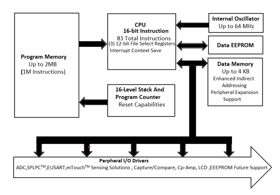
Figure. Peripherals
The PIC18 family combines maximum level of performance and integration for flexible use of 8-bit architecture.
- Internal Oscillator Up to 64 MHz.
- Flash Program Memory Up to 128 kB.
- Data EEPROM Up to 1 kB.
- SRAM Up to 8 kB.
- 32 Level Stack
- Hardware Stack Overflow and Underflow Reset Capabilities
- Vectored Interrupt Capability (VIC)
- Direct Access Memory (DAM) Controllers
- 12-bit ADC with Computation (ADC2), up to 43 channels
- Memory Access Partition (MAP)
- Device Information Area (DIA)
- Windowed Watch Dog Timer (WWDT)
- Three Complementary Waveform Generator (CWG)
- Four Configurable Logic Cell (CLC)
- Peripheral Pin Select (PPS)
- Two Comparators
- Zero Cross Detect (ZCD)
- Temperature Indicator On-chip
- Data Signal Modulator (DSM)
- 5-bit DAC
- Capacitive Voltage Divider (CVD)
- Up to four 10-bit PWMs
- Communication: UART, SPI, I2C, CAN, USB, Ethernet, LCD
- Extreme Low-Power (XLP)
Available in 18- to 100-pin Package
Q14) Write arithmetic and logical group of instructions?
A14)
- Arithmetic Instructions
ADDLW 8-bit; Add 8-bit number to WREG
ADDLW 0x32; Add 32H to WREG
ADDWF F, d, a; Add WREG to File (Data) Reg
Save result in W if d=0
Save result in F if d=1
ADDWF 0x20, 1; Add WREG to REG20 and save result in REG20
ADDWF 0X20,0; Add WREG to REG20 and save result in WREG
ADDWFC F, d, a; Add WREG to File Reg with carry and save result in W or F
SUBLW; Subtract WREG from literal
SUBWF F, d, a; Subtract WREG from File Reg
SUBWFB; Subtract WREG from File Reg with borrow
INCF; Increment File Reg
DECF; Decrement File Reg
COMF ; Complement File Reg
NEGF; Take two’s complement.
MULLW 8-bit; Multiply 8-bit and WREG save in PRODH -PRODL
MULWF F, a; Multiply WREG and File Reg save result in PRODH-PRODL
DAW; Decimal adjust WREG for BCD operations.
2. Logic Instructions:
ANDLW; AND literal with WREG
ANDWF F, d, a
IORLW 8-bit dats; Inclusive OR literal with WREG
IORWF F, d, a
XORLW 8-bit; Ex-clusive OR literal with WREG.
XORWF F, d, a
Q15) Write the branch control and call and return instructions?
A15)
1. Branch Instructions
- BC n; Branch if C flag = 1 within + or – 64 Words
- BNC n; Branch if C flag = 0 within + or – 64 Words (NO CARRY)
- BZ n; Branch if Z flag = 1 within + or – 64 Words
- BNZ n; Branch if Z flag = 0 within + or – 64 Words
- BN n; Branch if N flag = 1 within + or – 64 Words
- BNN n; Branch if N flag = 0 within + or – 64 Words
- BOV n; Branch if OV flag = 1 within + or – 64 Words
- BNOV n; Branch if OV flag = 0 within + or – 64 Words
- GOTO Address: Branch to 20-bit address unconditionally
2. Call and Return Instructions
- RCALL nn; Call subroutine within +or – 512 words
- CALL 20-bit, s; Call subroutine; If s = 1, save W, STATUS, and BSR
- RETURN, s; Return subroutine o; If s = 1, retrieve W, STATUS, and BSR
- RETFIE, s; Return from interrupt o; If s = 1, retrieve W, STATUS, and BSR
Q16) Mention all the components of PIC18 with the help of block diagram?
A16)

Figure. Architecture of PIC controller
The microcontroller architecture consists of CPU, I/O ports, memory organization, A/D converter, timers/counters, interrupts, serial communication, oscillator and CCP module
CPU (Central Processing Unit)
The PIC microcontroller CPU consists of the Arithmetic and Logic Unit, Memory Unit, Control Unit, accumulator and so on.
Arithmetic logic unit are mainly used for arithmetic operations and logical decisions. After processing, for storing the instructions memory is used. To control the internal and external peripherals, control unit is used to connect to CPU and accumulator is used for storing results.
Memory Organization
The memory module consists of RAM, ROM and STACK.
Random Access Memory (RAM)
RAM is an unstable memory used to store data temporarily in its registers. The registers of RAM are classified into Special Function Registers (SFR) and General-Purpose Registers (GPR).
- General Purpose Registers (GPR)
These registers are used for general purpose only.
- Special Function Registers
They are mainly used for special purposes only. These registers perform according to the functions assigned to them,
The STATUS register cannot be used for storing data, these registers are used for showing the operation or status of the program.

Figure. Memory Organization
Read Only Memory (ROM)
Read only memory is a stable memory used to store the data permanently. In PIC microcontroller ROM stores the instructions or programs. The microcontroller acts according to the program.
The ROM is also called as program memory, here the user writes the program and saves it permanently and executed by CPU. The microcontroller’s performance depends on the instruction executed by the CPU.
Electrically Erasable Programmable Read Only Memory (EEPROM)
Normally in ROM, we write the program only once and cannot use it multiple times. But, in EEPROM you can program the ROM multiple times.
Flash Memory
Flash memory also known as programmable read only memory (PROM) can read, write and erase the program thousands of times. PIC microcontroller uses this type of ROM.
Stack
When an interrupt occurs, first the PIC microcontroller must execute the interrupt and the existing process address that is being executed and store it in the stack. After completing the execution of the interrupt, the microcontroller calls the process with the help of address, which is stored in the stack and executes the process.
BUS
BUS is used for transfer and receive of data from one peripheral to another. It is classified into two types that is address and data bus.
Data Bus: It is used to transfer or receive the data.
Address Bus: Address bus transmits the memory address from peripherals to CPU. I/O pins are used to interface with external peripheral. UART and USART are serial communication protocols used for interfacing serial devices like GSM, GPS, Bluetooth, IR, and so on.

Figure. BUS