Unit 4
- Explain the construction of FET?
Unit 4
- Explain the construction of FET?
The semiconductor is the basis of all FETs. Depending on the channel we are using, i.e. N-channel or P-channel, the semiconductor specimen will be used. If we are designing N-channel JFETs, then the channel will be of an N-type semiconductor. And in the middle of the opposite phases of the specimen will be diffused with the P-type semiconductor.

The P-type semiconductor bar will act as a gate terminal. The opposite ends of the P-type semiconductor will be connected together to form a common gate terminal. Thus, there will be two P-N junctions on either side of the gate, and that will be termed as source and drain terminal.
Components of FETs
- Channel: This is the area in which majority charge carriers flow. When the majority charge carriers are entered in FET, then with the help of this channel only they flow from source to drain.
- Source: Source is the terminal through which the majority charge carriers are introduced in the FET.
- Drain: Drain is the collecting terminal in which the majority charge carriers enter and thus contribute in the conduction procedure.
- Gate: Gate terminal is formed by diffusion of a type of semiconductor with another type of semiconductor. It basically creates high impurity region which controls the flow of carrier from source to drain.
2. Explain the operation of FET?
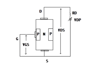
Gate are always reverse biased hence the gate current IG is practically zero. The source terminals is always connected to the end of the drain supply which provides necessary carrier ,in N-channel JFET source terminal is connected to the neagative end of the drain voltage source. The electrons flow from source to drain through the channel from D to S is started.
The current ID increases as Vdsincreases from zero on ward. This relationship between VDS and ID continuous till VDS reaches certain value called Pinch off
When VDS is equal to zero and VGS is decreased from zero the gate reverse bias increases , as the negative Vgs increases a stage reaches where two dip lections touch other in this condition the channel is said to be cut-off.
3. Explain the parameters of JFET?
At a fixed drain voltage, the drain current (ID) of a JFET depends on the gate to source voltage (VGS). If the gate to source voltage decreases from zero in n channel JFET, the drain current also gets decreased accordingly. The relation between gate to source voltage and drain current is given below.
ID = IDSS [ 1 – VGS/ VGS(off)] 2
After a certain gate to source voltage (VGS), the drain current ID becomes zero. This voltage is known as Cut Off Gate Voltage (VGS(off)).
When the gate terminal is grounded (VGS = 0) and positive drain to source voltage (VDS) is being increased slowly in case of n channel JFET, the drain current gets increased linearly. But after pinch-off voltage (Vp), the drain current would not be increased further and gets a constant value. This is the maximum drain current that can flow through the channel when the gate terminal is in ground potential. This current is fixed for a JFET and this is called shorted gated drain current and generally denoted by IDSS.
Transconductance is the ratio of change in drain current (δID) to change in the gate to source voltage (δVGS) at a constant drain to source voltage (VDS = Constant).
Gm = ∂ ID/ ∂ VGS at constant VDS
This value is maximum at VGS = 0. This is denoted by gmo. This maximum value (gmo) is specified in a JFET data sheet. The transconductance at any other value of gate to source voltage (gm) can be determined as follows. The expression of drain current (ID) is
ID = IDSS [ 1 – VGS/ VGS(off)] 2
Dynamic Output Resistance
This is the ratio of change of drain to source voltage (δVDS) to the change of drain current (δID) at a constant gate to source voltage (VGS = Constant). The ratio is
rd = ∂ VDS / ∂ ID at constant VGS
Denoted as rd.
The amplification factor is defined as the ratio of change of drain voltage (δVDS) to change of gate voltage (δVGS) at a constant drain current (ID = Constant).
μ=∂ VDS / ∂ VGS at constant ID
There is a relation between transconductance (gm) and dynamic output resistance (rd) and that can be established in the following way.
μ=∂ VDS / ∂ VGS = μ=∂ VDS / ∂ ID x ∂ ID / ∂ VGS
μ = rd x gm
4. Explain JFET as a switch?
FET can be used as a switch by operating it in two regions, they are cutoff and saturation region. When the VGS is zero the FET operates in saturation region and maximum current flows through it. Hence it is like a fully switched ON condition. Similarly, when the VGS applied is more negative than the pinch off voltage, FET operates in cutoff region and doesn’t allow any current flow through the device. Hence FET is in fully OFF condition.
FET Used as a Shunt Switch
- When the VGS applied is zero the FET is turned ON by operating in saturation region and its resistance is very small nearly 100 ohms. The output voltage across the across the FET is VOUT= Vin * {RDS/ (RD + RDS (ON))}. Since the resistance RD is very large, the output voltage is approximately considered as zero.
- When we apply the negative voltage which is equal to the pinch off voltage at the gate, FET operates in the cutoff region and acts as a high resistance device and the output voltage is equal to the input voltage.

FET Used as a Series Switch
In this circuit FET acts as a series switch. It acts as a closed switch if the control voltage is zero and open switch if control voltage is negative. When the FET is ON, the input signal will appear at the output and when it is OFF the output is zero.
5. Explain the construction of MOSFET?
The MOSFET can function in two ways
- Depletion Mode
- Enhancement Mode
Depletion Mode:
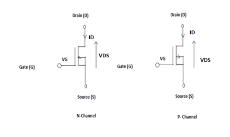 Depletion mode
When there is no voltage on the gate, the channel displays maximum conductance. As the voltage on the gate is either positive or negative, the channel conductivity decreases.
Enhancement Mode
When there is no voltage on the gate the device does not conduct. More is the voltage on the gate, the better the device can conduct.

Enhancement mode
6. Explain the working of MOSFET?
- The working of MOSFET depends upon the MOS capacitor. The MOS capacitor forms main part of MOSFET. The semiconductor surface at the below oxide layer is located between the source and drain terminal
- It can be inverted from p-type to n-type by applying a positive or negative gate voltage respectively. When we apply the positive gate voltage the holes present under the oxide layer with a repulsive force and holes are pushed downward with the substrate.
- The depletion region populated by the bound negative charges which are associated with the acceptor atoms. The electrons reach channel is formed.
- The positive voltage also attracts electrons from the n+ source and drain regions into the channel.
- Now, if a voltage is applied between the drain and source, the current flows freely between the source and drain and the gate voltage controls the electrons in the channel. Instead of positive voltage if we apply negative voltage, a hole channel will be formed under the oxide layer.

MOSFET construction
P-channel MOSFET
- The P- Channel MOSFET has a P- Channel region between source and drain. It is a four terminal device such as gate, drain, source, body. The drain and source are heavily doped p+ region and the body or substrate is n-type.
- The flow of current is positively charged holes. When we apply the negative gate voltage, the electrons present under the oxide layer are pushed downward into the substrate with a repulsive force.
- The depletion region populated by the bound positive charges which are associated with the donor atoms. The negative gate voltage also attracts holes from p+ source and drain region into the channel region.

Enhanced mode

Depletion mode
P-channel MOSFET
N- Channel MOSFET:
- The N-Channel MOSFET has a N- channel region between source and drain It is a four terminal device such as gate, drain , source , body. This type of MOSFET the drain and source are heavily doped n+ region and the substrate or body is P- type. The current flows due to the negatively charged electrons.
- When we apply the positive gate voltage the holes present under the oxide layer pushed downward into the substrate with a repulsive force. The depletion region is populated by the bound negative charges which are associated with the acceptor atoms. The electrons reach channel is formed.
- The positive voltage also attracts electrons from the n+ source and drain regions into the channel. Now, if a voltage is applied between the drain and source the current flows freely between the source and drain and the gate voltage controls the electrons in the channel.
- Instead of positive voltage if we apply negative voltage a hole channel will be formed under the oxide layer.
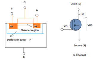
Enhancement mode
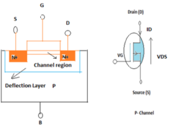
Depletion mode N channel MOSFET
7. Compare JFET ,BJT and MOSFET?

8. Explain PMOS circuit?
PMOS Logic
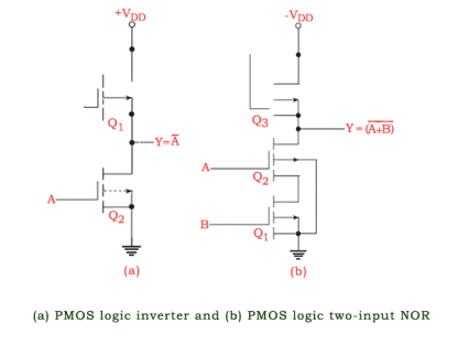
The PMOS logic family uses P-channel MOSFETS. Figure (a) shows an inverter circuit using PMOS logic .MOSFET Q1 acts as an active load for the MOSFET switch Q2.
For the circuit shown,GND and −VDD respectively represent a logic ‘1’ and a logic ‘0’ for a positive logic system.
When the input is grounded (i.e. logic ‘1’), Q2 remains in cut-off and −VDD appears at the output through the conducting Q1.
When the input is at −VDD or near −VDD, Q2 conducts and the output goes to near-zero potential (i.e. logic ‘1’). Figure (b) shows a PMOS logic based two-input NOR gate.
In the logic arrangement of Fig.(b), the output goes to logic ‘1’ state (i.e. ground potential) only when both Q1 and Q2 are conducting.
This is possible only when both the inputs are in logic ‘0’ state. For all other possible input combinations, the output is in logic ‘0’ state, because, with either Q1 or Q2 nonconducting, the output is nearly −VDD through the conducting Q3. The circuit of Fig.(b) thus behaves like a two-input NOR gate in positive logic.
9. Explain CMOS circuit?
CMOS:
For NMOS transistors, if the input is a 1 the switch is on, otherwise it is off.
On the other hand, for the PMOS, if the input is 0 the transistor is on, otherwise the transistor is off.
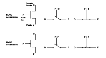
Here is a graphical representation of these facts: When a circuit contains both NMOS and PMOS transistors we say it is implemented in CMOS (Complementary MOS) .
Understanding the basics of transistors, we can now design a simple NOR gate.

Next figure shows the implementation in transistors of the NOR gate and how it works for different inputs (1 and 0). On the left there is the implementation, on the right the behavior.
The symbol VDD is the source voltage (or the logic 1), GND is the ground (or the logical 0).
To implement the rest of logical gates we analyze first the behavior of the transistors when connected in a “series” fashion or in a “parallel” way.
If we connect two NMOS transistors in series, we get the behaviour shown in next figure (the triangle in the bottom is a graphical representation of GND)

Next figure shows the behavior of the PMOSes when connected in series. (The horizontal line on top of the first transistor is a graphical representation of VDD).

10. Explain CMOS as a switch?
- CMOS as Switch.

CMOS circuits are constructed in such a way that all PMOS transistors must have either an input from the voltage source or from another PMOS transistor.
All NMOS transistors must have either an input from ground or from another NMOS transistor.