Unit - 2
Principles of scalable performance
Q1) What are performance metrics and measures?
A1) Performance metrics are a way to assess the quality of a computer design. To begin, it is critical to understand the metrics. Speed, capacity, cost, and energy consumption are the most likely factors of real-world performance measures. The world weighs these four variables in relation to a specific application or necessity before deciding on a computer. Among these four criteria, there is a trade-off. The performance of the CPU is the most important of the four. The term "capacity" refers to the amount of data that may be stored on a disk or in memory.
In a real-world scenario, a company wanting to purchase a computer(s) freezes the specifications based on its application expectations. The possibilities are then weighed and assessed. A common man's request may not be as detailed because off-the-shelf systems often meet his requirements in terms of capabilities, and so cost may be the primary consideration. In this chapter, we'll look at how computers function in terms of design.
The performance of a computer is determined by the system's constituent subsystems, which include software. Each subsystem's performance can be measured and fine-tuned. As a result, performance can be measured in terms of:
● CPU performance for Scientific application, Vector processing, Business application, etc. – Instructions per Second
● Graphics performance – Rendering - Pixels per second
● I/O Performance – Transactions Per Second
● Internet performance and more – bandwidth utilization in Mbps or Gbps
Both CPU and I/O performance are influenced by memory size, speed, and bandwidth. While CPU performance is almost assumed in any operating setting, in a Transaction processing environment, I/O performance is crucial.
System Performance Measurement
Performance, Execution Time, and Thruput are the three metrics for any system performance measure.
Total time taken for execution of a program = CPU Time + I/O Time + Others (like Queuing time etc.)
In general, the time it takes to run a program (whether it's a standard or an application program) is used as a proxy for system performance. This is known as "execution time."
Performance = 1/Execution Time
Thruput is the amount of work completed in a given amount of time.
CPU Time
CPU Time refers to the amount of time the CPU was occupied executing the program in question, i.e., the amount of time the program used the CPU to execute the instructions. Any program, we know, is transformed into a set of machine instructions that the CPU can execute. The more instructions in a program, the longer it takes the CPU to complete it. This is why, in addition to the target application software, we require a standard program to evaluate a system or CPU. Benchmark Program is the name given to such a standard program.
CPU Time in seconds (TCPU) = Number of Instructions in the program / average number of instructions executed per second by the CPU. OR
Number of Instructions in the program x Average clock cycles per instructions x time per clock cycle. This is written in the following rhythm.

Time per clock cycle = 1/ CPU clock frequency.
The most well-known CPU speed is y Ghz, which stands for CPU clock frequency.
Q2) Explain speedup performance laws?
A2) It was first presented at the AFIPS Spring Joint Computer Conference in 1967, and is named after computer scientist Gene Amdahl (an IBM and Amdahl corporation computer architect). Amdahl's argument is another name for it. It is a formula that calculates the theoretical increase in latency of task execution at a certain workload that may be predicted from a system with enhanced resources. In other words, it's a formula for determining the maximum increase that can be achieved by simply enhancing a single component of a system. It's commonly used in parallel computing to estimate the theoretical speedup when many processors are used.
Speedup
Speedup can be defined as the ratio of execution time for the entire task without using the enhancement to execution time for the entire task using the enhancement, or as the ratio of execution time for the entire task using the enhancement to execution time for the entire task without using the enhancement.
Amdahl’s Law
Remember that the speed up factor informs us of the relative advantage obtained when moving a task from a sequential to a parallel computer, and that performance does not scale linearly with the number of processors. Amdahl's law was derived in 1967 as a result of the above-mentioned saturation. According to Amdahl's law, a program has two sorts of operations: complete sequential operations that must be performed in a specific order and complete parallel operations that can be completed on numerous processors.
Consider the problem P, which requires the use of a parallel computer to solve. Amdahl's law states that there are two types of operations. As a result, the task will include both sequential and parallel procedures. We already know that solving a problem with a sequential machine and a sequential algorithm takes T (1) time. The time it takes to compute a sequential operation is a fraction of the total (α ≤ 1) execution time, i.e., T (1), while the time it takes to compute parallel operations is (1- α). As a result, S (N) can be calculated as follows:


Dividing by T (1)

Keep in mind that the value of is between 0 and 1. Let's try some different numbers of and see how the speed up factor changes as the number of processors grows. We discover that when the value of α: increases, the S(N) decreases.
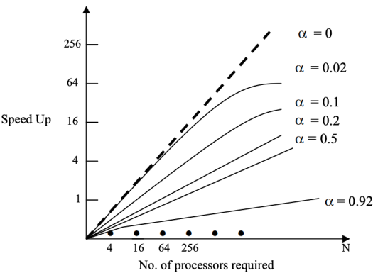
Fig 1: Speed-up vs. Number of Processors
In a parallel computer, the graph in Figure clearly shows that there is a bottleneck created by sequential operations. Even though the number of sequential operations is increased, the speed up factor S (N) decreases as the number of processors increases.
For a fixed value of N, say 500, the sequential fraction can be compared to the speed up factor S(N). The effect of Amdahl's law on the speed up factor is depicted in this diagram.
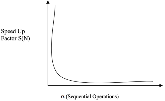
Fig 2: S (n) vs. α (Graph is not to scale)
The following are the results of Amdahl's law analysis:
1) In order to improve the performance of parallel computers, customized compilers must be designed with the goal of reducing the amount of sequential operations associated with the fraction.
2) Parallel computer makers were discouraged from producing large-scale devices with millions of processors.
Amdahl's law has one fundamental flaw that has been uncovered. The workload or problem size is always fixed, according to Amdahl's law, and the number of sequential operations is mostly constant. That is, it is assumed that the number of sequential and parallel processes is always distributed evenly. This scenario as depicted in the figure, as well as the ratio of sequential to parallel operations, are unaffected by the size of the problem.
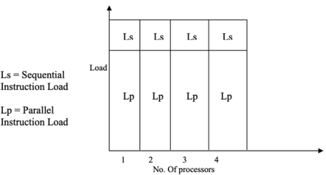
Fig 3: Fixed load for Amdahl’s Law
However, the number of simultaneous operations practically grows in proportion to the magnitude of the problem. The execution time will decrease when the number of processors is raised since the load is expected to be fixed according to Amdahl's law. Figure depicts the situation. This is an overview of how the processes work.
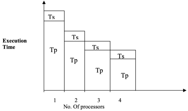
Fig 4: Execution Time decreases for Amdahl’s Law
Gustafson’s Law
For applications where response time is crucial, Amdahl's law is ideal. On the other hand, many applications necessitate a high level of accuracy in the generated output. The current situation has resulted in a significant boost in computing capability due to the addition of more processors to a parallel computer. As a result, the problem's magnitude can be expanded, i.e., the workload can be increased.
What is the mechanism behind this? Gustafson's Law removed the fixed-size constraint and intended to circumvent the sequential bottleneck found by Amdahl's Law by employing the concept of constant execution time. Gustafson examines this situation, which does not assume a fixed workload. As a result, Gustafson's Law posits that as the number of processors increases, the workload will increase significantly, but the overall execution time will remain constant, as shown in Figures a and b.
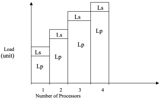
Fig 5a: Parallel Load Increases for Gustafson’s Law
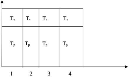
Fig 6b: Fixed Execution Time for Gustafson’s Law
According to Gustafson's Law, if a problem's number of parallel operations grows large enough, sequential operations will no longer be a bottleneck.
An example can be used to explain the statement of Gustafson's law. Consider a problem, P, that requires the use of a parallel computer to solve. Let Ts be the time taken to complete consecutive operations, which is deemed constant.
On a parallel computer with N processors, Tp (N, L) is the time it takes to run the parallel operations with L as the total load. T = Ts + Tp is the total time required to locate the answer to the problem. As a result, S (N) can be calculated as follows:


Tp (1, L) = N* Tp (N, L), i.e., the time it takes to execute parallel operations with a load of L on one processor is equal to N multiplied by the time it takes to perform parallel operations with a load of N on one processor. If for a given problem, is the fraction of sequential load, then

Substituting  we get,


Let us now write the whole S(N) equation in the form X. We obtain,


Let us now enter some values of and compute the speed up factor for rising values of, i.e., the sequential factor of work load for a fixed number of processors, say N. Figure depicts a pictorial representation of Gustafson's Law's effect on the speed up factor. As the value of grows, the speed up factor increases, as shown in the graph. The overhead induced by inter-processor communication is the reason of this drop.
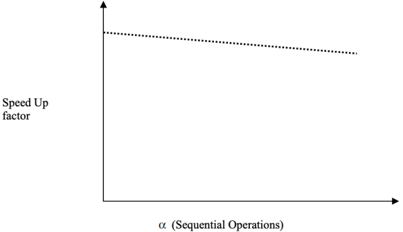
Fig 7: S (N) vs. α (Graph is not to scale)
Q3) What is RISC?
A3) A computer with a reduced instruction set (RIS) employs only simple commands that can be broken down into many instructions to perform low-level operations in a single CLK cycle, as the name suggests.
The RISC microprocessor stands for Reduced Instruction Set Computer, and its design offers a set of highly tailored instructions. The major purpose of this is to reduce the time it takes to execute instructions by restricting and optimizing the amount of commands used. Each command cycle thus employs a single clock cycle, with each clock cycle including three parameters: fetch, decode, and execute.
The type of processor is mostly used to combine numerous tough commands into a single, simpler command. The architecture of a RISC processor necessitates a large number of transistors, yet significantly minimizes instruction execution time. PowerPC, SUN's SPARC, RISC-V, Microchip PIC processors, and other RISC processors are some of the greatest examples.
Architecture
"Reduced Instruction Set Computer" is the abbreviation for "Reduced Instruction Set Computer." It's a fast-acting CPU design approach based on simple orders.
This is a condensed or simplified set of instructions. Every instruction is expected to complete extremely modest tasks here. The instruction sets of this machine are modest and straightforward, which aid in the compilation of more sophisticated commands. Each instruction is around the same length, and they're strung together to do complex tasks in a single operation. The majority of commands are executed in a single machine cycle. Pipelining is a critical technique for increasing the speed of RISC devices.
Q4) Write the characteristics of RISC?
A4) The following are some of the properties of RISC.
● The architecture of the pipeline.
● The number of instructions is both limited and decreasing.
● Memory access is granted to instructions such as load and store.
● There are fewer modes for addressing.
● The format of instruction can be reduced and is uniform.
Q5) Write the advantages of RISC?
A5) The following are some of the benefits of the RISC CPU.
● Because of the simple and restricted number of instructions, this processor performs well.
● This processor's design incorporates many transistors to save manufacturing costs.
● Because of its simplicity, the RISC processor allows instructions to use open space on a microprocessor.
● Because of this, it is incredibly basic when compared to other processors; it may complete its duty in a single clock cycle.
Q6) Write the disadvantages of RISC?
A6) The following are some of the drawbacks of a CISC CPU.
● Because the next commands may rely on the previous instruction for their implementation inside a cycle, the performance of this processor may differ depending on the executed code.
● Compilers and programmers regularly employ the complicated instruction.
● These processors require very fast memory to keep track of various instructions that use a large amount of cache memory to respond to commands in a short amount of time.
Q7) Write about CISC?
A7) It is a Complex Instruction Set Computer that was developed by Intel Corporation. This processor has a large number of instructions ranging from simple to complicated. These instructions are specified at the assembly language level, which means that they take longer to execute.
As the name suggests, a complex instruction set computer is one in which single instructions can execute many low-level tasks such as load from memory, arithmetic operation, and memory store, or are achieved by multi-step processes or addressing modes in single instructions.
As a result, this processor reduces the amount of instructions in each program while ignoring the number of cycles per instruction. It emphasizes the importance of publicly assembling complex instructions within the hardware, as hardware is always compared to software. CISC chips, on the other hand, are slower than RISC chips, but they use smaller instructions than RISC chips. AMD, VAX, System/360, and Intel x86 are some of the best examples of CISC processors.
Architecture
"Complex Instruction Set Computer" is the abbreviation for "Complex Instruction Set Computer." It's a CPU design strategy based on single commands capable of performing multi-step processes.
Small applications run on CISC computers. It has a large number of compound instructions to execute, which takes a lengthy time. A single set of instructions is safeguarded in this way in multiple steps; each instruction set contains over 300 individual instructions. The maximum number of machine cycles required to complete an instruction is two to 10. Instruction pipelining is difficult to implement in CISC.
Q8) Write the characteristics of CISC?
A8) The following are the main properties of the RISC processor.
● When compared to a single clock cycle, CISC may take longer to run the code.
● For basic compilation and complicated data structures, CISC offers high-level languages.
● It is collected using a larger number of addressing nodes and fewer registers, usually between 5 and 20.
● Less instruction is required while writing an application.
● Because the code is so brief, it only requires a little amount of RAM.
● It emphasizes hardware instructions when designing since it is faster to design than software.
● When compared to a single word, instructions are larger.
● It allows for easy assembly language programming.
Q9) Write the advantages of CISC?
A9) The following are some of the benefits of CISC.
● This processor will develop a mechanism for managing power consumption that adjusts clock speed and voltage.
● The compiler in the CISC processor requires a minimal amount of effort to convert a program or statement from high-level to assembly language, which is otherwise machine language.
● Different low-level jobs can be used to execute a single instruction.
● Because the code is brief, it doesn't take up a lot of memory.
● To execute the same instruction as RISC, CISC uses a smaller instruction set.
● On any CISC, the instruction can be stored in RAM.
Q10) Write the Disadvantages of CISC?
A10) The following are some of CISC's drawbacks.
● The CISC's existing guidelines are 20 percent within a program event.
● When compared to RISC processors, CISC processors execute every instruction cycle on every program relatively slowly.
● When compared to RISC, this processor uses a higher number of transistors.
● The CISC's pipeline execution will make it tough to use.
● Because of the slow clock, the machine's performance suffers.
Q11) What do you mean by super scalar?
A11) A superscalar processor is designed to create an execution cost for an individual sequential program that is greater than one instruction per clock cycle. Superscalar processor design refers to a set of techniques that allow a computer's central processing unit (CPU) to handle more than one instruction per cycle while running a single sequential program.
A superscalar architecture is made up of parallel execution units that may run instructions in parallel. This parallel architecture was initially implemented in RISC processors, which implement computing using short and simple instructions.
RISC processors have typically outperformed CISC processors running at the same megahertz due to their superscalar efficiency.
The superscalar instruction issue is the primary function of superscalar processing. Higher issue rates result in faster processor execution, but they also increase the limiting effect of control and data dependencies on processor design.
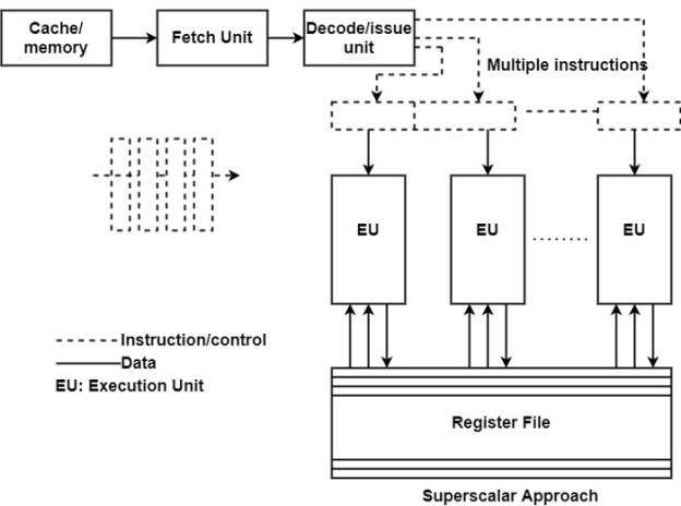
Fig 8: Superscalar processor
Q12) What is VLIW architecture?
A12) VLIW is an acronym for "Very Long Instruction Word." It's a type of instruction set architecture designed to maximize the performance of instruction-level parallelism (ILP).
CPU processors allow applications to specify which instructions should be executed in order, but VLIW processors allow programs to specify which instructions should be executed in parallel. This design is intended to allow for greater implementation without the complexity that some other designs entail.
Superscalar processors are strongly related with VLIW architectures. Both aim to speed up computing by taking advantage of instruction-level parallelism. Both have a nearly identical execution basis, with several execution units (EUs) controlling in simultaneously and either a unified register file for all data types or separate (split) register files for FX and FP data, as illustrated in the diagram.
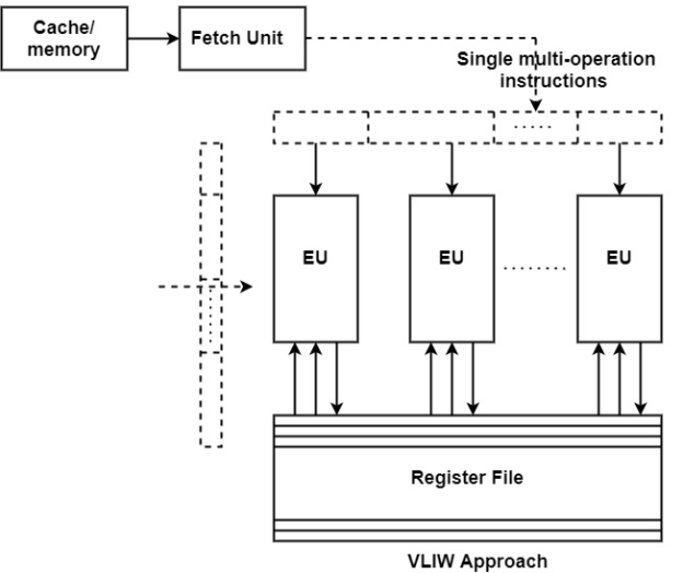
Fig 9: VLIW architecture
Q13) Write the difference between super scalar and VLIW architecture?
A13) Difference between super scalar and VLIW architecture
VLIW architecture | Superscalar processor |
A single multi-operation instruction is sent to the VLIW Architecture. | Except for a usual sequential flow of instructions, a superscalar processor can issue many instructions. |
To indicate what each execution unit should perform, the VLIW technique requires very large instruction words. | The superscalar processor receives sequential streams, which are decoded, and then issued multiple instructions to multiple execution units by the issues unit. The instruction unit of superscalar can send out 2 to 6 instructions every cycle. |
VLIW architecture processors demand code that is devoid of dependencies. | Dependency-free code is not expected to deal with dependencies utilizing specific hardware on superscalar processors. |
VLIW is a simpler version. | VLIW architecture is more sophisticated than superscalar processors with the same degree of parallelism. |
For static scheduling, VLIW is used. | For dynamic scheduling, Superscalar is employed. |
Q14) Explain cache memory organization?
A14) A cache memory is a quick random access memory where the computer hardware caches copies of data and instructions loaded from the main memory that are currently being used by applications. Because of the faster but more expensive implementation method used, the cache has a much lower access time than the main memory. The cache has a finite volume, which is due to the limitations of the technology used. If information fetched to the cache memory is utilized again, the access time to it will be substantially lower than if it were stored in the main memory, allowing the program to run faster.
The locality of data access seen during program execution results in the time efficiency of utilizing cache memories. We may see time and spatial localization here:
Time locality - The term "time locality" refers to the tendency for programs to reuse the same instructions and data over and over again over time intervals that are close together.
Space locality - The tendency to keep instructions and data utilized in a program under neighboring locations in the main memory across small spans of time is known as space locality.
Because of these locales, the information stored into the cache memory is reused multiple times, resulting in a significant reduction in program execution time. Cache is a multi-level memory that can be implemented.
Caches are frequently divided into two tiers in modern systems. A cache memory was installed outside a CPU in previous computer models (in separate integrated circuits than the processor itself). It was accessed through the processor's external system bus. The first level of cache memory in today's computers is built into the same integrated circuit as the processor.
It considerably improves the processor's cache cooperation. The second level of cache memory is also located in the integrated circuit of some microprocessors. The first level cache memory ranges in size from a few thousand to several tens of thousands of bytes. The volume of the second level cache memory is several hundred thousand bytes. A cache memory is maintained by a cache controller, which is a particular CPU subsystem.
If a computer system has a cache memory, the processor hardware sends the address to the cache memory first before accessing a main memory address to gather data or instructions. The cache control unit determines whether the requested data is stored in the cache. If this is the case, we get a "hit," and the requested data is retrieved from the cache. The steps involved in a read with a hit are depicted in the diagram below.
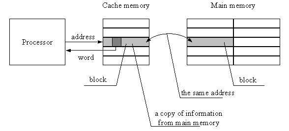
Fig 10: Implementation in cache memory on hit
We have a "miss" if the requested information is not in the cache, and the necessary information is fetched from the main memory to the cache and then to the requesting processor unit. The data is replicated in the cache as a larger block of a defined volume, rather than as individual words. A portion of the address of the block's beginning is always copied into the cache along with the information block. Following that, this portion of the address is read out during the identification of the correct information block. On "miss," the actions in a cache memory are shown below.

Fig 11: Implementation in cache memory on miss
The cache memory can be coupled to the processor and main memory in a variety of ways:
● As a separate subsystem linked to the system bus that connects the processor to the main memory,
● As a subsystem that sits in the middle of the processor and the main memory,
● Runs parallel with the main memory as a separate subsystem attached to the processor
For mapping information fetched from the main memory to the cache memory, there are three fundamental methods:
● Associative mapping
● Direct mapping
● Set-associative mapping.
Direct Mapping –
The simplest technique, known as direct mapping, maps each block of main memory into only one possible cache line. Or
In Direct mapping, assign each memory block to a specific line in the cache. If a line is previously taken up by a memory block when a new block needs to be loaded, the old block is trashed. An address space is split into two parts index field and a tag field. The cache is used to store the tag field whereas the rest is stored in the main memory. Direct mappings performance is directly proportional to the Hit ratio.
- i = j modulo m
- Where
- i=cache line number
- j= main memory block number
m=number of lines in the cache
For purposes of cache access, each main memory address can be viewed as consisting of three fields. The least significant w bits identify a unique word or byte within a block of main memory. In most contemporary machines, the address is at the byte level. The remaining s bits specify one of the 2s blocks of main memory. The cache logic interprets these s bits as a tag of s-r bits (most significant portion) and a line field of r bits. This latter field identifies one of the m=2r lines of the cache.

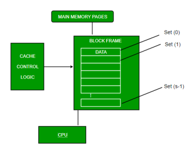
Fig 12: Direct mapping
Associative Mapping –
In this type of mapping, the associative memory is used to store content and addresses of the memory word. Any block can go into any line of the cache. This means that the word id bits are used to identify which word in the block is needed, but the tag becomes all of the remaining bits. This enables the placement of any word at any place in the cache memory. It is considered to be the fastest and the most flexible mapping form.
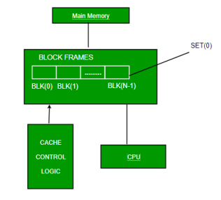
Fig 13: Associative mapping
Set-associative Mapping –
This form of mapping is an enhanced form of direct mapping where the drawbacks of direct mapping are removed. Set associative addresses the problem of possible thrashing in the direct mapping method. It does this by saying that instead of having exactly one line that a block can map to in the cache, we will group a few lines creating a set. Then a block in memory can map to any one of the lines of a specific set. Set-associative mapping allows that each word that is present in the cache can have two or more words in the main memory for the same index address. Set associative cache mapping combines the best of direct and associative cache mapping techniques.
In this case, the cache consists of several sets, each of which consists of several lines. The relationships are
m = v * k
i= j mod v
Where
i=cache set number
j=main memory block number
v=number of sets
m=number of lines in the cache number of sets
k=number of lines in each set

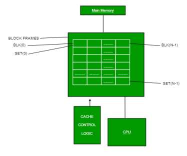
Fig 14: Set associative mapping
Q15) Describe shared memory organizations?
A15) A number of fundamental difficulties must be considered while designing shared memory systems.
Access control, synchronization, protection, and security are among them.
● Which processes have access to which resources is determined by access control.
● Accesses from sharing processes to shared resources are limited by synchronization limitations.
● Protection is a system feature that stops processes from gaining unauthorized access to other processes' resources.
One memory module that may be accessed by two processors is the most basic shared memory system.
Requests come in through the memory module's two ports.
Classification
A shared memory system can be categorized into the following categories depending on the interconnection network:
Uniform Memory Access (UMA)
The physical memory is shared equitably by all processors in this model. All processors have the same amount of time to access all memory words. A private cache memory may be available to each CPU. The same rule applies to peripheral devices.
A symmetric multiprocessor is one in which all of the processors have equal access to all of the peripheral devices. An asymmetric multiprocessor is one in which only one or a few processors have access to external devices.
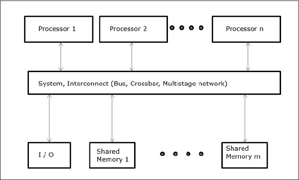
Fig 15: UMA
Non-uniform Memory Access (NUMA)
The access time in a NUMA multiprocessor model varies depending on the memory word's placement. Local memories are used to physically distribute shared memory among all CPUs. All local memories are combined to generate a global address space that can be accessed by all CPUs.
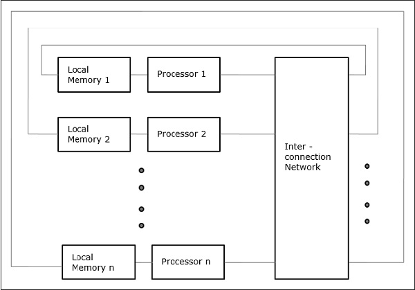
Fig 16: NUMA
Cache Only Memory Architecture (COMA)
A specific case of the NUMA model is the COMA model. All distributed main memories are transformed to cache memories in this step.
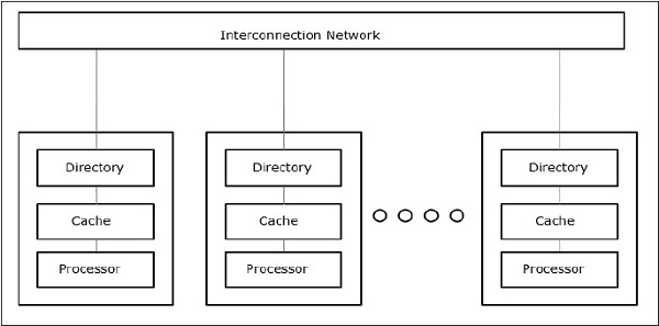
Fig 17: COMA
Q16) Explain memory hierarchy?
A16) A memory unit is an essential component in any digital computer since it is needed for storing programs and data.
Typically, a memory unit can be classified into two categories:
- The memory unit that establishes direct communication with the CPU is called Main Memory. The main memory is often referred to as RAM (Random Access Memory).
- The memory units that provide backup storage are called Auxiliary Memory. For instance, magnetic disks and magnetic tapes are the most commonly used auxiliary memories.
Apart from the basic classifications of a memory unit, the memory hierarchy consists of all of the storage devices available in a computer system ranging from the slow but high-capacity auxiliary memory to relatively faster main memory.
The following image illustrates the components in a typical memory hierarchy.
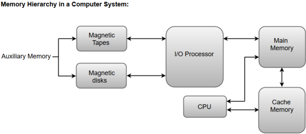
Fig 18: Memory hierarchy in a computer system
Auxiliary Memory
Auxiliary memory is known as the lowest-cost, highest-capacity, and slowest-access storage in a computer system. Auxiliary memory provides storage for programs and data that are kept for long-term storage or when not in immediate use. The most common examples of auxiliary memories are magnetic tapes and magnetic disks.
A magnetic disk is a digital computer memory that uses a magnetization process to write, rewrite and access data. For example, hard drives, zip disks, and floppy disks.
Magnetic tape is a storage medium that allows for data archiving, collection, and backup for different kinds of data.
Main Memory
The main memory in a computer system is often referred to as Random Access Memory (RAM). This memory unit communicates directly with the CPU and with auxiliary memory devices through an I/O processor.
The programs that are not currently required in the main memory are transferred into auxiliary memory to provide space for currently used programs and data.
I/O Processor
The primary function of an I/O Processor is to manage the data transfers between auxiliary memories and the main memory.
Cache Memory
The data or contents of the main memory that are used frequently by the CPU are stored in the cache memory so that the processor can easily access that data in a shorter time. Whenever the CPU requires accessing memory, it first checks the required data into the cache memory. If the data is found in the cache memory, it is read from the fast memory. Otherwise, the CPU moves onto the main memory for the required data.
Q17) What is cache performance?
A17) When the processor needs to read or write a location in the main memory, it first checks for a corresponding entry in the cache.
● If the processor finds that the memory location is in the cache, a cache hit has occurred and data is read from the cache
● If the processor does not find the memory location in the cache, a cache miss has occurred. For a cache miss, the cache allocates a new entry and copies in data from the main memory, then the request is fulfilled from the contents of the cache.
The performance of cache memory is frequently measured in terms of a quantity called the Hit ratio.
Hit ratio = hit / (hit + miss) = no. Of hits/total accesses
We can improve Cache performance using higher cache block size, higher associativity, reduce miss rate, reduce miss penalty, and reduce the time to hit in the cache.
Q18) Describe virtual machine?
A18) Virtual memory is an important idea in computer architecture that allows you to run huge, complex programs on a computer with a limited amount of RAM. Virtual memory allows a computer to juggle the competing needs of numerous programs within a limited quantity of physical memory. A PC with insufficient memory can run the same programs as one with plenty of RAM, but at a slower pace.
Physical vs Virtual Addresses
A computer's RAM is accessed using an address system, which is effectively a set of integers that identify each byte. Because the amount of memory on a computer varies, deciding which applications will run on it can be difficult. Virtual memory tackles this problem by treating each computer as if it had a lot of RAM and treating each software as if it only runs on the PC. For each program, the operating system, such as Microsoft Windows or Apple's OS X, generates a set of virtual addresses. Virtual addresses are translated into physical addresses by the operating system, which dynamically fits applications into RAM as it becomes available.
Paging
Virtual memory divides programs into pages of a predetermined size. The operating system loads all of a program's pages into RAM if the computer has enough physical memory. If not, the OS crams as much as it can into the available space and executes the instructions on those pages. When the computer finishes those pages, it puts the rest of the program into RAM, perhaps overwriting previous pages. Because the operating system handles these elements automatically, the software developer may focus on program functionality rather than memory issues.
Paging file
With virtual memory, the computer saves program pages that haven't been utilized in a while to a paging file on the hard drive. The file preserves the data contained in the pages, and the operating system reloads it when RAM becomes available if the program needs it again. When multiple programs compete for RAM, switching pages to the file can impair a computer's processing performance because it spends more time managing memory and less time doing valuable work. A computer should have enough RAM to handle the demands of multiple programs, reducing the amount of time it spends maintaining its pages.
Multiprogramming
Virtual memory combined with paging allows a computer to run multiple programs at the same time, nearly regardless of the amount of RAM available. This functionality, known as multiprogramming, is an important component of modern PC operating systems since it allows you to run multiple utility programs at the same time as your applications, such as Web browsers, word editors, email, and media players.
Memory protection
A computer without virtual memory can nevertheless run multiple programs at the same time, albeit one program may modify the data in another program, either accidentally or deliberately, if its addresses lead to the wrong program. Because a program never "sees" its physical addresses, virtual memory prevents this problem. The virtual memory manager safeguards data in one program from being tampered with by another.
Q19) Explain cache coherence?
A19) Data inconsistency in a multiprocessor system might arise between adjacent levels or within the same memory hierarchy level.
It is feasible to have numerous copies of any one instruction operand in a shared memory multiprocessor with a distinct cache memory for each processor: one in the main memory and one in each cache memory. When one copy of an operand is altered, all of the operand's other copies must be changed as well.
Cache coherence in computer architecture refers to the consistency of shared resource data that is stored in various local caches. When clients in a system keep caches of a shared memory resource, incoherent data can cause issues, which is especially true with CPUs in a multiprocessing system.
Consider the following scenario: both clients have a cached copy of a certain memory block from a previous read. If the client on the bottom updates/changes that memory block, the client on top may be left with an invalid memory cache without being notified of the change. Cache coherence aims to resolve such conflicts by keeping a consistent view of data values across several caches.
Mechanisms
Snooping and directory-based techniques are the two most popular strategies for maintaining coherency, each with its own set of benefits and cons. Because all transactions are a request/response observed by all computers, snooping-based protocols tend to be faster if appropriate bandwidth is available.
The disadvantage is that snooping cannot be scaled. Every request must be broadcast to all nodes in a system, which means the size of the (logical or physical) bus and the bandwidth it delivers must expand as the system grows. Directories, on the other hand, have greater latency (with a three-hop request/forward/respond cycle) but require far less bandwidth because messages are sent one-to-one rather than broadcast. As a result, this type of cache coherence is used in many bigger systems (>64 CPUs).
Snoopy
Snoopy protocols use a bus-based memory scheme to provide data consistency between cache and shared memory. Cache consistency is maintained using write-invalidate and write-update policies.
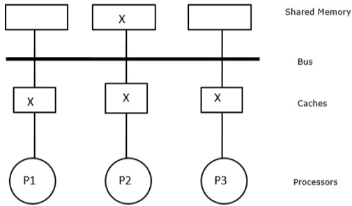
Fig 19: Consistent copies of block x are in shared memory and three processor caches
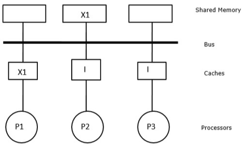
Fig 20: After a write invalidate operation by p1
We have three processors P1, P2, and P3 in this scenario, each with a consistent copy of data element 'X' in their local cache memory and shared memory (Figure-a). The write-invalidate protocol is used by processor P1 to store X1 in its cache memory. As a result, the bus invalidates all other copies. The letter 'I' stands for it (Figure-b). Invalidated blocks are also referred to as filthy blocks, as they should not be used. The write-update protocol uses the bus to update all cache copies. By using write back cache, the memory copy is also updated (Fig).
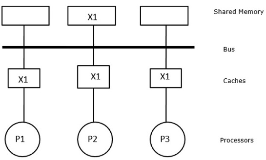
Fig 21: After a write update operation by p1
Directory-Based
The snoopy cache protocols must be adjusted to fit the network capabilities when using a multistage network to build a big multiprocessor with hundreds of processors. Because broadcasting is expensive in a multi-stage network, consistency commands are only issued to caches that have a copy of the block. This is why directory-based protocols for network-connected multiprocessors were created.
In a directory-based protocols system, data that has to be exchanged is stored in a central directory that keeps the caches in sync. The directory here serves as a filter, allowing the processors to request permission to load an element from primary memory into cache memory. If an entry is modified, the directory either updates it or invalidates the entries in other caches.
Q20) Write the difference between UMA and NUMA?
A20) Difference between UMA and NUMA
Sr. No. | Key | UMA | NUMA |
1 | Definition | UMA stands for Uniform Memory Access. | NUMA stands for Non Uniform Memory Access. |
2 | Memory Controller | UMA has single memory controller. | NUMA has multiple memory controllers. |
3 | Memory Access | UMA memory access is slow. | NUMA memory access is faster than UMA memory. |
4 | Bandwidth | UMA has limited bandwidth. | NUMA has more bandwidth than UMA. |
5 | Suitability | UMA is used in general purpose and time-sharing applications. | NUMA is used in real time and time critical applications. |
6 | Memory Access time | UMA has equal memory access time. | NUMA has varying memory access time. |
7 | Bus types | 3 types of Buses supported: Single, Multiple and Crossbar. | 2 types of Buses supported: Tree, hierarchical. |