Unit - 2
AM & FM Receivers
Q1) A sinusoidally modulated ordinary AM waveform is shown below.
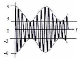
(a) Determine the modulation index. (b) Calculate the transmission efficiency. (c) Determine the amplitude of the carrier which must be added to attain a modulation index of 0.3.
A1)
(a) Using 
(b) 
(c) Using  the new required carrier amplitude
So, the amplitude of the carrier should be added by 4 to achieve the 0,3 modulation index.
Q2) The efficiency μ of a single-tone AM signal is defined as the percentage of the total power carried by the sidebands, that is: where Psig is the power carried by the sidebands and Pt is the total power of the AM signal. (a) Find μ for AM modulation index ma=0.5. (b) Show that for a single-tone AM, μmax is 33.3% at ma =1.
A2)
 carrier power
 sideband power
Thus 
(a) for 
(b)  occurs at
Q3) The output signal from an AM modulator is: s(t) = 5cos(1800π t) + 20cos (2000π t) + 5cos (2200π t)
(a) Determine the modulation index.
(b) Determine the ratio of the power in the sidebands to the power in the carrier.
A3)
(a) 

Thus modulation index is 0.5
(b) Carrier power=200
Sideband power =25
Sideband power to carrier power ratio=0.125
Q4) Assume that the transmitter circuitry limits the modulated output signal to a certain peak voltage value, say X volts. By employing this transmitter, show that the sideband power of a DSB-SC signal with a peak voltage of X is four times that of an AM (DSB-LC) signal having the same peak voltage and 100% modulation index, and is half that of a SSB-SC signal having the same peak voltage
A4)
(1) DSB-SC: s(t)=Ax(t) cos 
Peak voltage=

(2) DSB-LC: s(t)=A[1+x(t)] cos 
Peak voltage=

(3)SSB-SC: s(t)=Ax(t) cos 
Peak voltage=

Hence the sideband power of a DSB-SC signal is four times that of an AM(DSB-LC) signa and is half(or one-quarter( that of a SSB-BC signal.
Q5) A single-tone modulating wave m(t) =Amcos(2π fmt) is used to generate the VSB modulated wave: s(t)=α AmAccos[2π (fc + fm) t] + AmAc(1-α)cos[2π (fc - fm) t], where α is a constant (α ≤ 1), Ac is the amplitude of carrier, and fc is the frequency of carrier.
(a) Express s(t) in the form of I(t)cos(2πfc t)+ Q(t)sin(2πfc t), where I(t) and Q(t) are called the in-phase and quadrature components.
(b) What is the value of the constant α for which s(t) reduces to a DSB-SC modulated wave?
(c) What are the values of the constant α for which s(t) reduces to a SSB modulated wave?
(d) The VSB wave s(t), plus a carrier Ac cos(2πfc t), is passed through an envelope detector. Determine the distortion produced
A5)
(a) Expanding s(t) we get

(b)Because 
When  the VSB is reduced to DSB-SC.
(c) When  the VSB is reduced to DSB-SC.
(d) the output from envelope detector:


Q6) A radio receiver used in the AM system is shown below. The mixer translates the carrier frequency fc to a fixed IF of 455kHz by using a local oscillator of frequency fLO. The broadcast-band frequencies range from 540kHz to 1600kHz.
(a) Determine the range of tuning that must be provided in the local oscillator
(i) when fLO is higher than fc (superheterodyne receiver) and
(ii) when fLO is lower than fc.
(b) Based on the results obtained in (a), explain why the usual AM radio receiver uses a superheterodyne system.
A6)
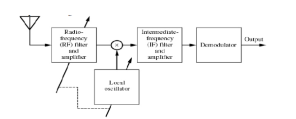
(a) when  the required tuning range of the local oscillator is 995kHz – 2055kHz.
When  the required tuning range of the local oscillator is 45kHz – 1145kHz.
(b) The frequency ratio, that is the ratio of the highest  to the lowest
  is 2.07 for
  and 13.47 for
  (superheterodyne) is preferred.
Q7) A particular version of AM stereo uses quadrature multiplexing. Specifically, the carrier Ac cos(2π fc t) is used to modulate the sum signal m1(t) = Vo + mL(t) + mR(t) where Vo is a DC offset included for the purpose of transmitting the carrier component, mL(t) is the left-hand audio signal, and mR(t) is the right-hand audio signal. The quadrature carrier Acsin(2π fc t) is used to modulate the difference signal m2(t) = mL(t) - mR(t)
(a) Show that an envelope detector may be used to recover the sum mL(t) + mR(t) from the quadrature-multiplexed signal. How would you minimize the signal distortion produced by the envelope detector?
(b) Show that a synchronous/coherent detector can recover the difference signal, mL(t) -mR(t). (c) How are the desired mL(t) and mR(t) finally obtained?
A7)
The transmitted signal is

(a) The envelope detection output:

If we choose a large value of 
(b) Multiply s(t) by  and followed by a low-pass filter
  is obtained.
(c) With the known values of  and
and  . It is easy to get
  and
and  .
.
Q8) A normalized sinusoidal signal a(t) has a bandwidth of 5,000 Hz and its average power is 0.5W. The carrier Acos2πfct has an average power of 50W. Determine the bandwidth and the average power of the modulated signal if the following analog modulation scheme is employed:
(a) single-side band modulation with suppressed carrier modulation (SSBSC), which is generated by phase-shift method with the given carrier;
(b) double-side band with suppressed carrier modulation (DSB-SC);
(c) AM or double-side band with large carrier (DSB-LC) with a modulation index of 0.8.
A8)
As the average power of the carrier is
 so the A=10

Bandwidth is 5000Hz
b) DSB-SC:


Bandwidth is 10000Hz
c) AM or DSB-LC:


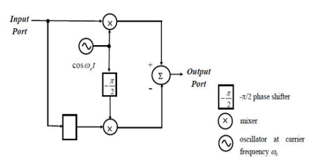
Q9) Consider the following circuit:
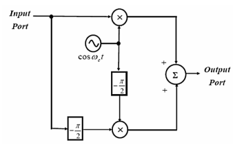
(i) An upper-sideband single-sideband (SSB) can be generated by feeding a message signal m(t) into the input port of the above circuit. This is known as phase-shifted method for SSB signal generation. Determine the modulated signal s(t) at the output port.
(ii) Suggest one appropriate modification of the above circuit so that the modified circuit can be used to demodulate the upper-sideband SSB signal obtained in part(b)(i) and retrieve the message signal m(t). Prove and verify your modified circuit as an upper-sideband SSB signal demodulator.
A9)


Q10) Consider the following circuit with an input signal, v(t), an amplifier with gain K, a sinusoidal carrier signal at ωc, and two nonlinear devices:
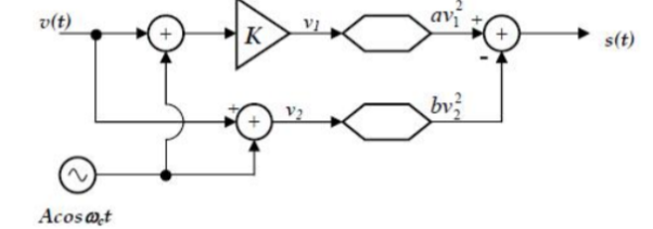
(a) Express the output signal s(t) in terms of v(t), A, K, cos (ωct), a and b. (b) Determine the choice of the gain K so that the above circuit performs as a DSB-SC modulator without output filtering.
A10)
(a) 

(b)  (assume ab>0)
Q11) Explain the demodulation technique for DSBFC?
A11) Square Law Detector
It can be used to detect modulated signals of small magnitude, so that the operating point may be chosen in the non-linear portion of the V-I characteristic of diode. A DC supply voltage is used to get a fixed operating point in the non-linear region of diode characteristics. The output diode current is hence given by the non-linear expression:
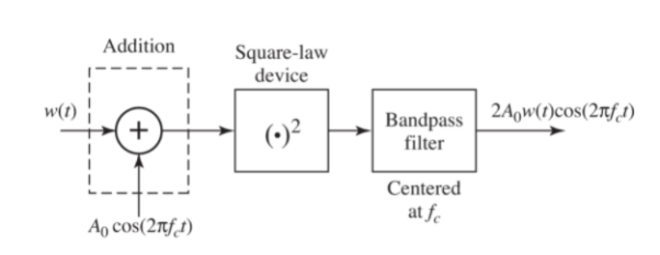
i = a v(t) +bv2(t)
v(t)= [A+ x(t)cos(2πfct)]
This current will have terms at baseband frequencies as well as spectral components at higher frequencies. The low pass filter comprised of the RC circuit is designed to have cut-off frequency as the highest modulating frequency of the band limited baseband signal. It will allow only the baseband frequency range, so the output of the filter will be the demodulated baseband signal.
Envelope Detection
This method is used in most of the commercial AM radio receivers.
An envelope detector is as shown below.
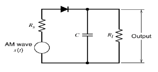
- During the positive half cycles of the input signals, the diode D is forward biased and the capacitor C charges up rapidly to the peak of the input signal.
- When the input signal falls below this value, the diode becomes reverse biased and the capacitor C discharges through the load resistor RL.
- The discharge process continues until the next positive half cycle.
- When the input signal becomes greater than the voltage across the capacitor, the diode conducts again and the process is repeated.
- The charge time constant (rf+Rs)C must be short compared with the carrier period, the capacitor charges rapidly and there by follows the applied voltage up to the positive peak when the diode is conducting.
That is the charging time constant shall satisfy the condition,
(rf + Rs) C << 1/ fc
On the other hand the discharging time constant RLC must be long enough to ensure that the capacitor discharges slowly through the load resistor RL between the positive peaks of the carrier wave .
The discharge time constant shall satisfy the condition
1/fc << RL C << 1/W
Where ‘W’ is band width of the message signal. The result is that the capacitor voltage or detector output is nearly the same as the envelope of AM wave.
Q12) What is coherent or synchronous detector. Explain quadrature null effect?
A12) The process of extracting an original message signal from DSBSC wave is known as detection or demodulation of DSBSC.
Coherent Detector
Here, the same carrier signal used for generating DSBSC signal is used to detect the message signal. Hence, this process of detection is called as coherent or synchronous detection. Consider the following diagram of the coherent detector.
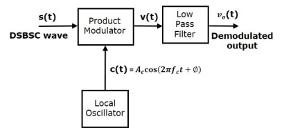
In this process, the message signal is extracted from DSBSC wave by multiplying it with a carrier, which has the same frequency and the phase of the carrier used in DSBSC modulation. The resulting signal is then passed through a Low Pass Filter. Output of this filter is the desired message signal.
Let the DSBSC wave be
s(t) = Ac cos(2πfct) m(t) ------- (1)
The output of the local oscillator is
c(t)=Ac cos(2πfct+ϕ) -------(2)
Where, ϕ is the phase difference between the local oscillator signal and the carrier signal, which is used for DSBSC modulation.
From the figure, we can write the output of product modulator as
v(t)=s(t)c(t) -----------------(3)
v(t)=Ac cos(2πfct) m(t) Ac cos(2πfct+ϕ) --------------(4)
=Ac2 / 2 cos(2πfct)cos(2πfct+ϕ)m(t) -----------------(5)
=Ac2/2[cos(4πfct+ϕ)+cosϕ]m(t) ----------------- (6)
v(t)=Ac2/2 cosϕm(t)+Ac2/2cos(4πfct+ϕ)m(t) ----------------(7)
In the above equation, the first term is the scaled version of the message signal. It can be extracted by passing the above signal through a low pass filter.
Therefore, the output of low pass filter is
v0t=Ac2/2cosϕ m(t) ------------- (8)
The demodulated signal amplitude will be maximum, when ϕ=0.
That’s why the local oscillator signal and the carrier signal should be in phase, i.e., there should not be any phase difference between these two signals.
The demodulated signal amplitude will be zero, when ϕ=±900 This effect is called as quadrature null effect.
Q13) The Noise Density at the output terminals of an arbitrary amplifier with a gain factor of 100 and is 7×10-19 Watts/Hz. What is the Noise Temperature (Te) of this system?
A13)
The Noise Density at the output is given by:
No = G k Tout -----------------(1)
Where:
Tout = To + Te
K = 1.3806 x 10 -23
T0 = 290 0
Te = No/Gk – To
Te =217 0 Kelvin.
Friss Formula
The available noise power at the output of the amplifier 1 is
Pno1 = F1 G1 kTo Bn --------------(1) and this is available to amplifier 2.
Amplifier 2 has noise of its own (F2-1) kTo Bn of its own at its input , hence total available noise power at the input of amplifier 2 is given by
Pni2 = F1 G1 kTo Bn + + (F2-1) kTo Bn ------------------------(2)
Now since the noise of amplifier2 is represented by its equivalent input source , the amplifier itself can be regarded noiseless and of available power gain G2 so that the available noise output of amplifier 2 is
Pno2 = G2 Pni2
= G2 ( F1G1 kTo Bn + (F2-1) kTo Bn)) -----------------------(3)

The overall available power of the two amplifiers in cascade is
G = G1 G2 -----------(4)
Let the overall noise factor be F then output noise power can also be expressed as
Pno = FG kTo Bn ---------------------(5)
Equating the two equations for output noise (1) and (2)
F1G1 kToBn + (F2-1) kTo Bn = FG kToBn---------------------(6)
F1G1 + (F2-1) = FG -----------------------(7)
F1G1 + (F2-1) = FG -----------------------------(8)
F= F1G1/G + (F2-1) /G ------------------------------------(9)
Where G = G1G2 -------------------(10)
F = F1 + (F2-1)/G ------------------------------------(11)
By making G1 large, the noise contribution of the second stage can be made negligible and F1 must also be small so that the noise contribution of the first amplifier is low.
The argument is easily extended for additional amplifiers to give
F = F1 + (F2-1)/G1 + (F3-1)/G1G2.
This is known as Friss Formula.
Q14) What is noise figure and noise temperature?
A14)
Noise Figure
- The Noise figure is the amount of noise power added by the electronic circuit at the receiver to the thermal noise power from the input of the receiver.
- The thermal noise at the input to the receiver passes through the demodulator.
- This noise present in the receiver channel cannot be removed.
- The noise figure of circuits in the receiver such as amplifiers and mixers, adds additional noise to the receive channel.
- This raises the noise floor at the demodulator.
Noise Temperature
Noise Temperature provides a way to describe how much noise a system adds to a signal.
To know the total noise performance of the system, calculate an equivalent temperature (Te) that would yield the same noise power at the output via additional thermal noise.
It is important to realize that the noise temperature of a component describes the additional noise that the component inserts onto a signal before it is amplified, as shown in the figure below.
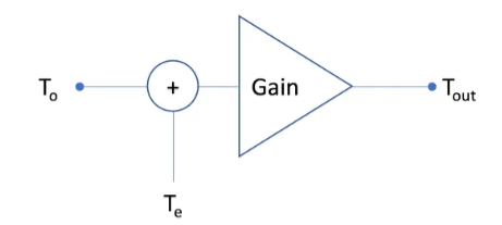
- The reason we use Noise Temperature is because it allows us an easy way to combine the effects of an antenna and a receiver together.
- Antennas are responsible for receiving signals and passing them to a radio receiver where they can be amplified and demodulated.
- Antennas also receive noise from the environment as they are in as part of the received signal.
- Antenna Temperature defines the mount of noise that can be measured at an antenna’s terminals.
Q15) What is noise? Explain types of noise?
A15) A signal may be contaminated along the path by noise. Noise may be defined as any unwanted introduction of energy into the desired signal.
In radio receivers noise may produce hiss in the loud speaker output. Hence noise is random and unpredictable.
Noise is produced in both external and internal to the system.
External noise includes
Atmospheric noise (lightining)
Galatic noise(thermal radiation)
Industrial noise (from motors, ignition)
We can minimize or eliminate external noise by proper system design.
Internal noise is generated inside the system.It is resulted due to random motion of charged particles in resistors, conductors and electronic devices.
With proper design it can be minimized but never can be eliminated.
Types of Noise
- White Noise
- Thermal noise
- Shot noise
- Partition noise
- Low frequency or flicker noise
- Burst noise
- Avalanche noise
- White Noise
One of the important random processes is the white noise process. Noises in many practical situations are approximated by the white noise process.
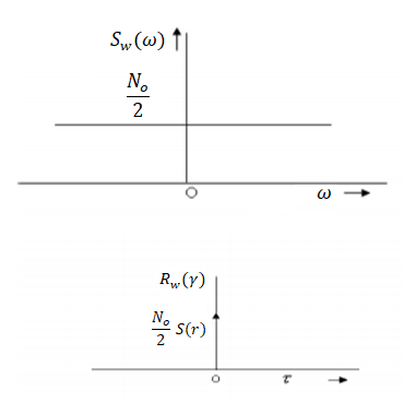
White noise plays an important role in modelling of WSS signals. A white noise process W(t) is a random process that has constant power spectral density at all frequencies.
Thus
S w(w) = N0/2 ----------------(1) - ∞<w<∞
Where No is real constant and called the intensity of the white noise. The corresponding autocorrelation is given by
Rw( = N/2
= N/2  (
( where
where  (
( is the Dirac delta.
The average power of white noise
P wg = E W 2 = 1/2π dw -> ∞
The autocorrelation function and the PSD of white noise process is shown in Figure.
- Thermal Noise
Thermal noise is the electronic noise generated by thermal agitation of charge carriers inside an electrical conductor in equilibrium, which happens regardless of any applied voltage.
Movement of electrons will form kinetic energy in the conductor related to temperature in the conductor.
When the temperature increases the movement of electrons increases and current flows through the conductor.
Current flows due to free electrons which create noise voltage n(t).
Noise voltage is influenced by temperature hence it is called thermal noise.
Calculate the thermal noise power available from any resistor at room temperature (290K) for a bandwidth of 1Mhz . Calculate also the corresponding noise voltage given that R = 50 Ω.
Pn = 1.38 x 10 -23 x 290 x 10 6
= 4 x 10 -15.
En2 = 4 x 50 x 1.38 x 10 -23 x 290
= 0.895 µ V
- Shot Noise
- Shot noise arises because the current consists of a vast number of discrete charges.
- The continuous flow of these discrete pulses gives rise to almost white noise. There is a cut-off frequency by the time it takes for the electron or other charge carrier to travel through the conductor.
- Unlike thermal noise, this noise is dependent upon the current flowing and has no relationship to the temperature at which the system is operating.
- Shot noise is more apparent in devices such as PN junctions. The electrons are transmitted randomly and independently of each other.
- Partition Noise
When the circuit is to divide in between two or more paths then the noise generated is known as Partition noise. The reason for this generation is random fluctuation in the division.
- Flicker Noise
Flicker noise or modulation noise is the one appearing in transistors operating at low audio frequencies. Flicker noise is proportional to the emitter current and junction temperature. However, this noise is inversely proportional to the frequency.
- Burst Noise
Burst noise consists of step-like transitions suddenly between two or more discrete voltages or current levels.
Each shift in offset voltage or current lasts for millisecond to seconds . It is also known as popcorn noise because of the popping or crackling sound it produces in audio circuits.
- Avalanche Noise
Avalanche noise is the noise produced when a junction diode is operated at the onset of avalanche break down , a semiconductor junction phenomenon in which the carriers having high voltage gradient develop sufficient energy to dislodge additional carriers through physical impact creating ragged current flow.
Q16) Explain the need and working of phase discriminator?
A16) The FOSTER-SEELEY DISCRIMINATOR is also known as the PHASE-SHIFT DISCRIMINATOR. It uses a double-tuned rf transformer to convert frequency variations in the received fm signal to amplitude variations. These amplitude variations are then rectified and filtered to provide a dc output voltage. This voltage varies in both amplitude and polarity as the input signal varies in frequency. A typical discriminator response curve is shown in figure. The output voltage is 0 when the input frequency is equal to the carrier frequency (fr). When the input frequency rises above the center frequency, the output increases in the positive direction. When the input frequency drops below the center frequency, the output increases in the negative direction.
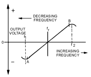
The output of the Foster-Seeley discriminator is affected not only by the input frequency, but also to a certain extent by the input amplitude. Therefore, using limiter stages before the detector is necessary.
Circuit Operation of a Foster-Seeley Discriminator
Figure shows a typical Foster-Seeley discriminator. The collector circuit of the preceding limiter/amplifier circuit (Q1) is shown. The limiter/amplifier circuit is a special amplifier circuit which limits the amplitude of the signal. This limiting keeps interfering noise low by removing excessive amplitude variations from signals. The collector circuit tank consists of C1 and L1. C2 and L2 form the secondary tank circuit. Both tank circuits are tuned to the center frequency of the incoming fm signal.
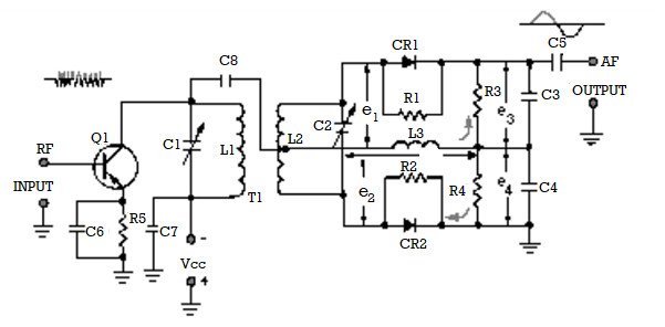

Choke L3 is the dc return path for diode rectifiers CR1 and CR2. R1 and R2 are not always necessary but are usually used when the back (reverse bias) resistance of the two diodes is different. Resistors R3 and R4 are the load resistors and are bypassed by C3 and C4 to remove rf. C5 is the output coupling capacitor.
CIRCUIT OPERATION AT RESONANCE—The operation of the Foster-Seeley discriminator can best be explained using vector diagrams that show phase relationships between the voltages and currents in the circuit. Let's look at the phase relationships when the input frequency is equal to the center frequency of the resonant tank circuit. The input signal applied to the primary tank circuit is shown as vector ep. Since coupling capacitor C8 has negligible reactance at the input frequency, rf choke L3 is effectively in parallel with the primary tank circuit. Also, because L3 is effectively in parallel with the primary tank circuit, input voltage ep also appears across L3. With voltage ep applied to the primary of T1, a voltage is induced in the secondary which causes current to flow in the secondary tank circuit. When the input frequency is equal to the center frequency, the tank is at resonance and acts resistive. Current and voltage are in phase in a resistance circuit, as shown by is and ep. The current flowing in the tank causes voltage drops across each half of the balanced secondary winding of transformer T1. These voltage drops are of equal amplitude and opposite polarity with respect to the center tap of the winding. Because the winding is inductive, the voltage across it is 90 degrees out of phase with the current through it. Because of the center-tap arrangement, the voltages at each end of the secondary winding of T1 are 180 degrees out of phase and are shown as e1 and e2 on the vector diagram. The voltage applied to the anode of CR1 is the vector sum of voltages ep and e1, shown as e 3 on the diagram. Likewise, the voltage applied to the anode of CR2 is the vector sum of voltages ep and e 2, shown as e4 on the diagram. At resonance e3 and e4 are equal, as shown by vectors of the same length. Equal anode voltages on diodes CR1 and CR2 produce equal currents and, with equal load resistors, equal and opposite voltages will be developed across R3 and R4. The output is taken across R3 and R4 and will be 0 at resonance since these voltages are equal and of appositive polarity. The diodes conduct on opposite half cycles of the input waveform and produce a series of dc pulses at the rf rate. This rf ripple is filtered out by capacitors C3 and C4.
OPERATION ABOVE RESONANCE—A phase shift occurs when an input frequency higher than the center frequency is applied to the discriminator circuit and the current and voltage phase relationships change. When a series-tuned circuit operates at a frequency above resonance, the inductive reactance of the coil increases and the capacitive reactance of the capacitor decreases. Above resonance the tank circuit acts like an inductor. Secondary current lags the primary tank voltage, ep. Notice that secondary voltages e 1 and e2 are still 180 degrees out of phase with the current (iS) that produces them. The change to a lagging secondary current rotates the vectors in a clockwise direction. This causes el to become more in phase with ep while e2 is shifted further out of phase with ep. The vector sum of ep and e2 is less than that of ep and e1. Above the center frequency, diode CR1 conducts more than diode CR2. Because of this heavier conduction, the voltage developed across R3 is greater than the voltage developed across R4; the output voltage is positive.
OPERATION BELOW RESONANCE—When the input frequency is lower than the center frequency, the current and voltage phase relationships change. When the tuned circuit is operated at a frequency lower than resonance, the capacitive reactance increases and the inductive reactance decreases. Below resonance the tank acts like a capacitor and the secondary current leads primary tank voltage ep. This change to a leading secondary current rotates the vectors in a counter clockwise direction. From the vector diagram you should see that e2 is brought nearer in phase with ep, while el is shifted further out of phase with ep. The vector sum of ep and e2 is larger than that of e and e1. Diode CR2 conducts more than diode CR1 below the center frequency. The voltage drop across R4 is larger than that across R3 and the output across both is negative.
Q17) What is dual conversion super heterodyne receiver?
A17) Need:
When choosing the intermediate frequency for a superheterodyne radio receiver there is a trade-off to be made between the advantages of using a low frequency IF or a high frequency one as each has its own advantages and disadvantages.
- High frequency IF: For any intermediate frequency within a superhet radio the image response appears at a frequency equal to twice that of the IF away from the wanted one. Making the IF as high as possible enables the image response to be as far away as possible from the wanted signal, making the RF filtering to remove the unwanted response much easier, and much better levels of rejection can be obtained. Accordingly the use of an intermediate frequency with a high frequency provides good image rejection. Some modern HF band communications receivers that cover frequencies up to 30 MHz, may have first IFs of 50 or 60 MHz to ensure a god level of performance.
- Low frequency IF: The advantage of choosing a lower frequency IF is that the filters that provide the adjacent channel rejection are lower in frequency. The use of a low frequency IF enables the performance to be high, while keeping the cost low. Although filters like ceramic filters, crystal filters and the like have improved immeasurably in recent years, costs and performance are still better at lower frequencies. Certainly if 60 MHz IFs are used for the main selectivity, then the filters at these frequencies would not perform as well, and they would be considerably more expensive.
There are two conflicting requirements, which cannot be easily satisfied using a single intermediate frequency. The solution is to use a double conversion super heterodyne topology to provide a means of satisfying both requirements. Sometimes even a triple conversion super het may be used to provide the required performance and flexibility.
Fixed frequency first oscillator:
It was widely used in many amateur radio receivers where a band of 500 kHz was normally tuned to cover a particular band. This form of receiver was able to provide significant improvements in stability performance as well as improved image rejection, although the wideband first IF stage was often open to some direct pick-up.
A switched crystal oscillator in the first conversion would provide a stable first local oscillator used to provide the local oscillator for the first conversion. A band pass filter would be used to provide selectivity and allow a band of frequencies to be passed.
The second local oscillator would allow tuning over the range allowed by the band pass filter. When further coverage is required, the first, crystal controlled oscillator, would need to be switched to the next crystal. In this way continuous coverage can be obtained, with large number of crystals.
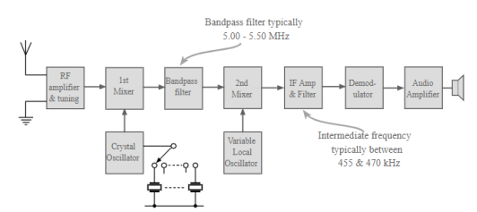
Block diagram of a superheat with crystal controlled first conversion
Apart from providing high levels of image rejection, this concept gave considerably improved levels of frequency stability for receivers of the time.
Tuned first oscillator: This is the most usual form of double conversion superheterodyne receiver. The first conversion uses a variable frequency oscillator which converts the signal to the first IF.
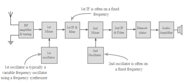
Double conversion superheat using a frequency synthesizer for the first LO
Although little selectivity is generally provided in the first IF, often a filter known as a roofing filter may be used to provide some adjacent channel filtering. This prevents very strong adjacent channel signals from overloading the later stages of the IF.
However the main selectivity is still provided in the lower frequency IF stages.
The first local oscillator would typically be some form of frequency synthesizer as these are widely used and relatively cheap and easy to implement.
They have excellent stability and can be programmed via a microprocessor enabling facilities like keypad frequency entry, tuning controlled via a processor, scanning and much more.
Q18) Define the following terms, Selectivity, sensitivity, fidelity, IFRR, tracking of a super heterodyne receiver?
A18) Sensitivity of a receiver is defined as the ability of the receiver to amplify weak signals received by the receiver. It is the voltage that must be applied at the input terminals of the receiver to achieve a minimum standard output at the output of the receiver. The factors that determine the sensitivity of super heterodyne receiver are –
- Gain of the IF amplifier
- Noise figure of the receiver
- Gain of RF amplifier
Image Frequency Rejection:
In standard broadcast receiver the local oscillator frequency is made higher than the signal frequency by an amount equal to intermediate frequency(IF).
Therefore fo =fs + fi.
When fo and fs are mixed the difference in frequency is equl to fi which is passed and amplified by the IF stage.
If a frequency fsi (fo+fi) ie fsi=fo+2fi appears at the input of the mixer then it will produce the sum and difference of frequencies regardless of the inputs. The term fsi is called the image frequency defined by signal frequency plus twice the intermediate frequency. This is also amplified which results in interference.
The rejection of an image frequency by a single tuned circuit is the ratio of gain at signal frequency to the gain at image frequency. It is given by
α =  Q2
Q2  2 where
  = fsi/fs – fs/fsi
And Q = loaded Q of the tuned circuit.
IFRR:
It is a numerical measure of the ability of a preselector to reject the image frequency.
Mathematically expressed as,
IFRR =( 1+Q2 ρ2 ) 1/2
Where ρ= (fim/fRF) – (fRF/fim)
Q = quality factor of a pre-selector
Once an image frequency has down-converted to IF, it cannot be removed.
In order to reject the image frequency, it has to be blocked prior to the mixer stage. That is the bandwidth of the pre-selector must be sufficiently narrow to prevent image frequency from entering the receiver
Tracking:
The super heterodyne receiver has number of tunable circuits which must be tuned correctly if any given station is to be received. The ganged tuning is employed to do this work which mechanically couples ann tuning circuits so that only one tuning control or dial is required. Usually there are three tuned circuits
Antenna
Mixer tuned.
Local Oscillator tuned.
All these circuits must be tuned to get proper RF input and to get IF frequency at the output of the mixer. The process of tuning circuits to get desired output is called tracking
Selectivity:
- It refers to the ability of a receiver to select the signal of desired frequency. It is obtained by tuning circuits. These are LC circuits tuned to resonate at desired frequency. The Q of these tuned circuits determine the selectivity.
- Selectivity shows the attenuation that the receiver offers at frequencies near to the one to which it is tuned.
- A good receiver isolates the desired signal in RF spectrum. The bandwidth of the tuned circuit is given by
- BW = fr/Q. Where fr is the resonant frequency. To have narrow bandwidth and better selectivity the Q of the tuned circuit must be hugh.
Fidelity:
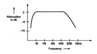
- Fidelity refers to the ability of the receiver to reproduce all the modulating frequencies as shown in figure.
- The fidelity at lower modulating frequencies is determined by the low frequency response of the IF amplifier and the fidelity at higher modulating frequencies which is determined by the high frequency response of the IF amplifier.
- Fidelity is difficult to obtain in AM receiver because good fidelity requires more bandwidth resulting in poor selectivity.
