Unit - 1
INTRODUCTION TO MOS TRANSISTOR
Q1) What is Channel-length modulation? Explain the NMOS or n-type MOS and PMOS?
A1) The current between drain and source terminals is constant and independent of the applied voltage over the terminals. This is not entirely correct. The effective length of the conductive channel is actually modulated by the applied VDS, increasing VDS causes the, depletion region at the drain junction to grow, reducing the length of the effective channel.
NMOS
NMOS is built on a p-type substrate with n-type source and drain diffused on it. Here, the majority carriers are electrons. When a high voltage is applied to the gate, the NMOS conducts and when low voltage is applied to the gate, it does not conduct. NMOS is faster than PMOS, as the carriers are electrons that travel twice as fast as the holes.
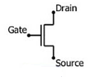
Fig 1 NMOS Symbol
PMOS
P-MOS consists of P-type Source and Drain diffused on an N-type substrate. Here, majority carriers are holes. When a high voltage is applied to the gate, the PMOS does not conduct and when a low voltage is applied, it conducts. These devices are more immune to noise than NMOS devices.
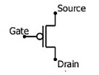
Fig 2 PMOS symbol
Q2) What is Latch – up? How it can be prevented?
A2) Latch up is a condition in which the parasitic components give rise to the establishment of low resistance conducting paths between VDS and VSS with disastrous results. Careful control during fabrication is necessary to avoid this problem.
- An increase in substrate doping levels with a consequent drop in the value of Rpsubs.
- Reducing Rnwell by control of fabrication parameters and ensuring a low contact resistance to VDD.
- By introducing guard rings
Q3) What is body effect in MOSFETs? Or Define body bias effect. Also explain the N channel and p-channel MOSFET?
A3) The threshold voltage VT is not a constant with respect to the voltage difference between the substrate and the source of the MOS transistor. This effect is called the body effect or substrate bias effect.
The most basic element in the design of large- scale integrated circuit is the transistor. The type of transistor available is the Metal-Oxide-Semiconductor Field Effect Transistor (MOSFET). These transistors form as a sandwich'' consisting of semiconductor layer, a slice or wafer, which from a single crystal of silicon; a layer of silicon dioxide and a layer of metal. These layers are patterned in a manner which permits transistors to be formed in the semiconductor material the substrate'.
The diagram showing a typical MOSFET
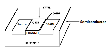
Figure 3. MOS Transistor
The transistor consists of three regions, labelled as the source'', gate'' and the drain''. The area labelled as the gate region forms a sandwich consisting of the underlying substrate material. The electrical charge or current can flow from the source to the drain depending on the charge applied to the gate region. The semiconductor material in the source and drain region are doped'' with a different type of material than in the region under the gate, so NPN or PNP type structure exists between the source and drain region of a MOSFET.
In Figure 4 (a), the source and drain regions are doped with N type material and the substrate doped with P type material. Such a transistor is called an N channel MOSFET.
If they were doped with P type material, and the substrate doped with N type material as in Figure 4 (b), the device would be called a P channel MOSFET.
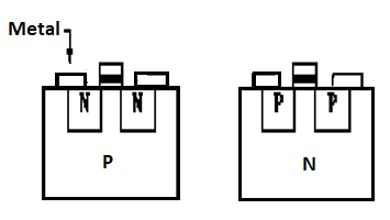
Figure 4(a) N channel MOSFET (b) P channel MOSFET
Q4) Define propagation delay of CMOS Inverter. Draw the CMOS circuit and also write the logic output of the circuit?
A4) The inverter propagation delay (tP) is defined as the average of the low-to-high (tPLH) and the high to low (tPHL) propagation delays:
Tp= tplh+tphl/2
Propagation delays tPLH and tPHL are defined as the times required for output voltage to reach the middle between the low and high logic levels, i.e. 50 % of VDD in our case of CMOS logic.
CMOS
CMOS stands for “Complementary Metal Oxide Semiconductor”.
It is one of the most popular technology in the chip design industry and is used today to form integrated circuits for various applications.
Computer memories, CPUs and cell phones make use of this technology due to various advantages. This technology uses both P and N channel semiconductor devices.
CMOS Applications
- Computer memories, CPUs
- Microprocessor designs
- Flash memory chip designing
- Used to design application specific integrated circuits (ASICs)
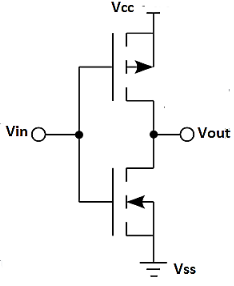
Fig 5 CMOS
The inverter circuit as shown in the figure above. It consists of PMOS and NMOS FET. The input A serves as the gate voltage for both transistors.
The NMOS transistor has an input from Vss (ground) and PMOS transistor has an input from Vdd. The terminal Y is output. When a high voltage (~ Vdd) is given at input terminal (A) of the inverter, the PMOS becomes open circuit and NMOS switched OFF so the output will be pulled down to Vss.
When a low-level voltage (<Vdd, ~0v) applied to the inverter, the NMOS switched OFF and PMOS switched ON. So the output becomes Vdd or the circuit is pulled up to Vdd.
INPUT | LOGIC INPUT | OUTPUT | LOGIC OUTPUT |
0 V | 0 | Vdd | 1 |
Vdd | 1 | 0 v | 0 |
Q5) Draw the DC transfer characteristics of CMOS inverter
A5) The VTC is divided into five regions(1-5) for easy of understanding. The above shown curve is possible when both T1 and T2 are matched for optimum operation. Optimum operation is achieved when Vin = Vdd/2 we get Vout = Vdd/2 . This can be achieved by adjusting width and length of both T1 and T2 as other parameters like mobility, oxide capacitance vary between different technologies.
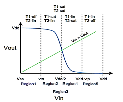
Fig 6 DC Transfer Characteristics
Region-1
In this, the input is in the range of (0,Vtn).
- NMOS is in cutoff as Vgs < Vtn
- PMOS is in linear as Vgsp < Vtp and Vdsp > Vgsp -Vtp.
- Zero current flows from supply voltage and the power dissipation is zero.
Region-2
Here, the input is in the range of (Vtn,Vdd/2).
- NMOS is in saturation as Vgs > Vtn and Vout >Vin – Vtn.
- PMOS is in linear region as Vdsp > Vgsp -Vtp.
- Since both the transistors are conducting some amount of current flows from supply in this region.
Region-3
Here the input voltage is Vdd/2. At this point the output voltage is Vdd/2. Here both the NMOS and PMOS are in saturation and the output drops drastically from Vdd to Vdd/2. At this point a large amount of current flows from the supply.
- NMOS is in saturation as Vgs > Vtn and Vout >Vin - Vtn.
- PMOS is in saturation as Vgsp < Vtp and Vdsp < Vgsp -Vtp.
- Large amount of current is drawn from supply and hence large power dissipation.
Region-4
In this region the input voltage is in the range of (Vdd/2 , Vdd-Vtp). Here the PMOS remains in saturation as Vout < Vin - Vtp and Vgsp < Vtp. But the NMOS moves from saturation to linear region since the drain to source voltage now is less than Vgsn-Vtn.
- NMOS is in linear as Vgs > Vtn and Vout < Vin - Vtn.
- PMOS is in saturation as Vgsp < Vtp and Vdsp < Vgsp -Vtp.
- A medium amount of current is drawn as NMOS is in linear region and power dissipation is low.
Region-5
In this region the input voltage is in the range of (Vdd-Vtp,Vdd). Here the PMOS moves from saturation to cutoff as the Vgsp is so high that Vgsp > Vtp. The NMOS still remains in linear as the drain to source voltage now is less than Vgsn-Vtn.
- NMOS is in linear as Vgs > Vtn and Vout < Vin - Vtn.
- PMOS is in cutoff as Vgsp > Vtp.
- Zero current flows from the supply and hence the power dissipation is zero.
Q6) Explain the circuit of RC delay model using n-MOS and p-MOS?
A6)
- The RC delay model is a metric used in VLSI design to calculate the signal delay between the input voltage and output voltage of the input signal.
- The input signal is a step function. In this case the transistor can be considered as a switch in series with a resistor.
- A unit nMOS transistor is characterized with resistance or effective resistance, R= Vds/Ids
- Let’s consider a k times transistor unit, here the resistor of the single transistor is R/k, k is the constant here. PMOS transistor has a bigger resistance – 2R .
- NMOS transistors are characterized with higher mobility than pMOS transistors. If the transistor is velocity-saturated, its current and resistance does not depend on the channel length.
- Let’s consider a transistor with gate capacitance C. For a k unit cell, gate capacitance of the transistor is kC.
- Diffusion capacitance depends on the size of drain or source, but with the most common approximation it is also C.
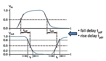
Fig 7 Time Delay
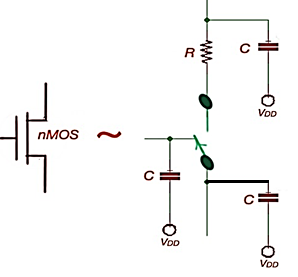
Fig 8 RC Circuit
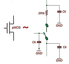
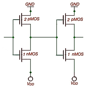
Fig 9: Equivalent RC circuits
Q7) What are the layout design rules?
A7) Design rules are the communication link between the designer specifying requirements and the fabricator who materializes them. Design rules are used to produce workable mask layouts from which the various layers in silicon will be formed or patterned.
The design rules primary address two issues:
1. The geometrical reproduction of features that can be reproduced by the mask making and lithographical process, and
2. The interaction between different layers.
There are primarily two approaches in describing the design rules.
1. Linear scaling is possible only over a limited range of dimensions.
2. Scalable design rules are conservative. This, results in over dimensioned and less dense design.
3. This rule is not used in real life.
1. Scalable Design Rules (e.g. SCMOS, λ-based design rules):
In this approach, all rules are defined in terms of a single parameter λ. The rules are so chosen that a design can be easily ported over a cross section of industrial process, making the layout portable. Scaling can be easily done by simply changing the value of. The key disadvantages of this approach are:
2. Absolute Design Rules (e.g. μ-based design rules): In this approach, the design rules are expressed in absolute dimensions (e.g. 0.75μm) and therefore can exploit the features of a given process to a maximum degree. Here, scaling and porting is more demanding, and has to be performed either manually or using CAD tools. Also, these rules tend to be more complex especially for deep submicron.
The fundamental unity in the definition of a set of design rules is the minimum line width. It stands for the minimum mask dimension that can be safely transferred to the semiconductor material. Even, for the same minimum dimension, design rules tend to differ from company to company, and from process to process. Now, CAD tools allow designs to migrate between compatible processes.
Q8) Describe the equation for source to drain current in the three regions of operation of a MOS transistor and draw the VI characteristics
A8) We have two types of FETs. They are Enhancement mode and depletion mode transistor. Also, we have PMOS and NMOS transistors.
(i) In Enhancement mode transistor channel is going to form after giving a proper positive gate voltage. We have NMOS and PMOS enhancement transistors.
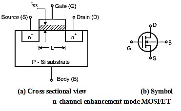
Fig 12 n-channel enhancement type MOSFET
(ii) In Depletion mode transistor channel will be present by the implant. It can be removed by giving a proper negative gate voltage. We have NMOS and PMOS depletion mode transistors
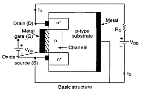
Fig 13 p-channel depletion MOSFET
Three regions of operation of a MOS transistor
a) Vgs > Vt Vds = 0 Since Vgs > Vt and Vds = 0 the channel is formed but no current flows between drain and source.
b) Vgs > Vt Vds < Vgs - Vt This region is called the non-saturation Region or linear region where the drain current increases linearly with Vds. When Vds is increased the drain, side becomes more reverse biased and the channel starts to pinch. This is called as the pinch off point.
c) Vgs > Vt Vds > Vgs - Vt This region is called Saturation Region where the drain current remains almost constant. Even if the Vds is increased more and more, the increased voltage gets dropped in the depletion region leading to a constant current. The typical threshold voltage for an enhancement mode transistor is given by Vt = 0.2 * Vdd.

Curve
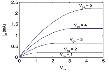
Fig 14 Vds v/s Ids
Q9) What is Elmore delay?
A9) The Elmore delay analysis model estimates the delay from a source (root) to one of the leaf nodes as the sum of the resistance in the path to the ith node multiplied by the capacitance present at the end of the branch.
Most circuits can be represented as an RC circuit with no loops. As we already stated, the Elmore delay estimates the delay from a source (root) to one of the leaf nodes as the sum of the resistance in the path to the ith node multiplied by the capacitance present at the end of the branch. In other words, the propagation delay from a switching source (root) to an ith branch node is given as the product of the capacitance “Ci” of the node with the sum of the resistance from the source to the node, Ris.
Tpd =
Ris = sum of resistance from source to node i
The 2nd order RC equivalent circuit we considered in the RC delay model:
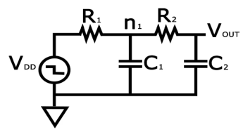
Fig.15 RC Equivalent
The Elmore delay for Vout is given as tpd = R1C1+(R1+ R2) C2, which is similar to the delay expression gotten for the two-time constant (TTC) approximation model we discussed in the last article.
Let's consider a driver—i.e., a gate that charges or discharges a node or, in other words, a gate that is connected to the input of another gate. For our example, we'll look at a driver which is w-times the unit size which is driving an m-identical inverter. The equivalent RC circuit is shown in Figure below
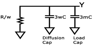
Fig.16 Equivalent Model

From above equation if we denote the fan-out of the drive to be the ratio between the load capacitance (3mc) and the input capacitance (3wc), we get the following:
h=3mc/3wc=m/w
Tpd = (1+h)3RC
Where τ=3RC.
Q10) What is linear delay model?
A10) Normalized delay of a gate can be expressed as the sum of parasitic delay and effort delay. The effort delay depends on the fan-out of the gate, here is a logical effort.
Electrical effort is a situation when a gate is driving identical to itself gates is said to have an electrical effort or fan-out. In case if the load consists of gates different from driving gate, the electrical effort of fan-out can be found by formula, here is the capacitance of the driving gate, and is the capacitance of the load gates that are being driven.
Q11) What is delay in logic gates explain through waveform?
A11) The propagation delay of a logic gate e.g. Inverter is the difference in time (calculated at 50% of input-output transition), when output switches, after application of input.
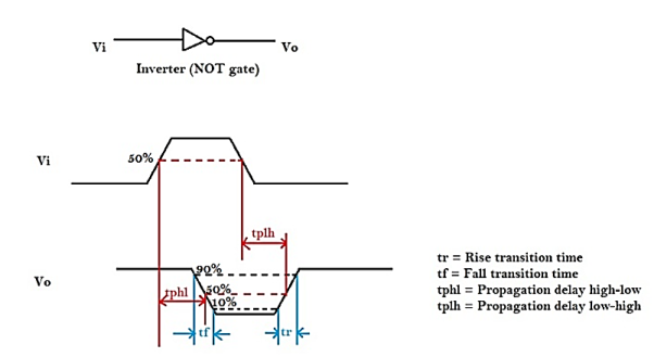
Fig 17 Propagation Delay
In the above figure, there are 4 timing parameters. Rise time (tr) is the time, during transition, when output switches from 10% to 90% of the maximum value. Fall time (tf) is the time, during transition, when output switches from 90% to 10% of the maximum value. Many designs could also prefer 30% to 70% for rise time and 70% to 30% for fall time. It could vary upto different designs.
The propagation delay high to low (tpHL) is the delay when output switches from high-to-low, after input switches from low-to-high. The delay is usually calculated at 50% point of input-output switching, as shown in above figure.
Now, in order to find the propagation delay, we need a model that matches the delay of inverter. As we have seen above, the switching behavior of CMOS inverter could be modeled as a resistance Ron with a capacitor CL, a simple first order analysis of RC network will help us to model the propagation delay.
Q12) How does scaling reduces the design area. What are the various types of scaling?
A12) The reduction in dimension of MOSFET or CMOS which reduces the size of chip is called as scaling. There are many advantages of scaling such as switching speed increases, chip size reduces and power dissipation reduces.
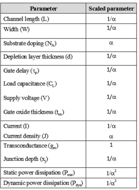
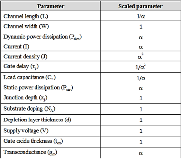
There are three types of scaling as constant voltage, constant field and lateral scaling. In constant voltage scaling, VDD is kept constant, and the process is scaled. For constant field scaling, the device dimensions are scaled by the parameter λ.
Constant Field Scaling:
In constant field scaling the scaled devices are obtained by scaling all dimensions of transistor, device voltages and the doping concentration densities by factor . The effect of scaling is shown in Table below
Constant Voltage Scaling:
In constant voltage scaling the supply voltage VDD is kept constant while the process is scaled. The effect of scaling is shown in Table below.
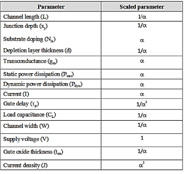
With constant voltage scaling the electric field increases which has led to the development of the lateral double diffused structures.
Lateral Scaling: In lateral scaling only the gate length is scaled. This is also called as the "gate shrinking". The effect of this scaling of parameters is shown in Table below.
Q13) What are stick diagrams taking any example draw one stick diagram?
A13) Another popular method of symbolic design is "Sticks" layout. In this, the designer draws a freehand sketch of a layout, using coloured lines to represent the various process layers such as diffusion, metal and polysilicon. Where, polysilicon crosses diffusion, transistors are created and where metal wires join diffusion or polysilicon, contacts are formed. This notation indicates only the relative positioning of the various design components. The absolute coordinates of these elements are determined automatically by the editor using a compactor.
The compactor translates the design rules into a set of constraints on the component positions, and solve a constrained optimization problem that attempts to minimize the area or cost function. The advantage of this symbolic approach is that the designer does not have to worry about design rules, because the compactor ensures that the final layout is physically correct. The disadvantage of the symbolic approach is that the outcome of the compaction phase is often unpredictable. The resulting layout can be less dense than what is obtained with the manual approach. In addition, it does not show exact placement, transistor sizes, wire lengths, wire widths, tub boundaries.
For example, stick diagram for CMOS Inverter is shown below

Fig 18 Stick Diagram of CMOS inverter
Q14) What are transmission gates show its symbol and circuit diagram?
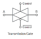
A14) When PMOS and NMOS devices together are connected in parallel then a basic bilateral CMOS switch is created and is known as a “Transmission Gate”. Here, the transmission gate is symmetrical, or bilateral, that is, the input and output are interchangeable. This bilateral operation is shown in the transmission gate symbol below which shows two superimposed triangles pointing in opposite directions to indicate the two signal directions.
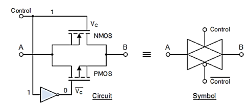
Fig 19 Transmission gate
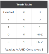
Both MOS transistors are connected back-to-back in parallel with an inverter used between the gate of the NMOS and PMOS to provide the two complementary control voltages. When the input control signal, VC is LOW, both the NMOS and PMOS transistors are cut-off and the switch is open. When VC is high, both devices are biased into conduction and the switch is closed.
When VC = 1, the transmission gate acts as a “closed” switch,
When VC = 0, it operates as a voltage-controlled switch.
The bubble of the symbol indicating the gate of the PMOS FET.
Symbol
Truth Table
Boolean Expression B = A.Control
Q15) How multiple threshold drops can be avoided in pass transistor?
A15)
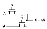
Fig 20 Pass Transistor
A popular and widely-used alternative to complementary CMOS is pass-transistor logic, which attempts to reduce the number of transistors required to implement logic by allowing the primary inputs to drive gate terminals as well as source/drain terminals. This is in contrast to logic families that we have studied so far, which only allow primary inputs to drive the gate terminals of MOSFETS. Pass-transistor gates cannot be cascaded by connecting the output of a pass gate to the gate input of another pass transistor.

Fig 21 Pass transistor output (Drain/Source) terminal should not drive other gate terminals to avoid multiple threshold drops.
Q16) Explain the CMOS inverter logic design?
A16)
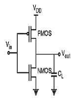
Fig 22: CMOS inverter
- It consists of PMOS and NMOS FET.
- The input A serves as the gate voltage for both transistors.
- The NMOS transistor has an input from Vss (ground) and PMOS transistor has an input from Vdd. The terminal Y is output.
- When a high voltage (~ Vdd) is given at input terminal (A) of the inverter, the PMOS becomes open circuit and NMOS switched OFF so the output will be pulled down to Vss.
- The truth table of inverter is:
A | Y = A’ |
0 | 1 |
1 | 0 |

Fig.23: NOT gate