Unit - 6
Nonlinear applications of op-amp
Q1) Explain hysteresis comparator?
A1)
A hysteresis comparator is operated by applying positive feedback to the comparator. The potential difference between High and Low output voltages and the feedback resistor are adjusted to change the voltage that is taken as a comparison reference to the input voltage for +IN terminal. The width of variation in the reference voltage is the hysteresis width. In this circuit the signal to -IN terminal and the output is inverted.
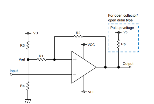
Q2) Explain its operation with hysteresis?
A2)
Operation with hysteresis:
Since a margin is provided between the High-to-Low and Low-to-High thresholds, no chattering occurs in the output even when a signal is input at a voltage near the threshold voltages.
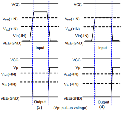
When the input signal (-IN) is applied at a voltage sufficiently higher than VthH(+IN) and VthL(+IN), the output is varied according to Vref as a threshold.
When the input signal (-IN) is applied at a voltage equivalent to VthH(+IN) or above, no chattering occurs since the output will not respond unless the input falls below the threshold at VthL(+IN).
VthL is the voltage switching from Low to High.
VthH is the voltage switching from High to Low.
Q3) Explain zero crossing detector?
A3)
An op-amp detector that has the ability to detect the change from positive to negative or negative to a positive level of a sinusoidal waveform is known as a zero- crossing detector.
It is also known to be a square wave generator as the applied input signal is converted into a square wave by the zero -crossing detector.
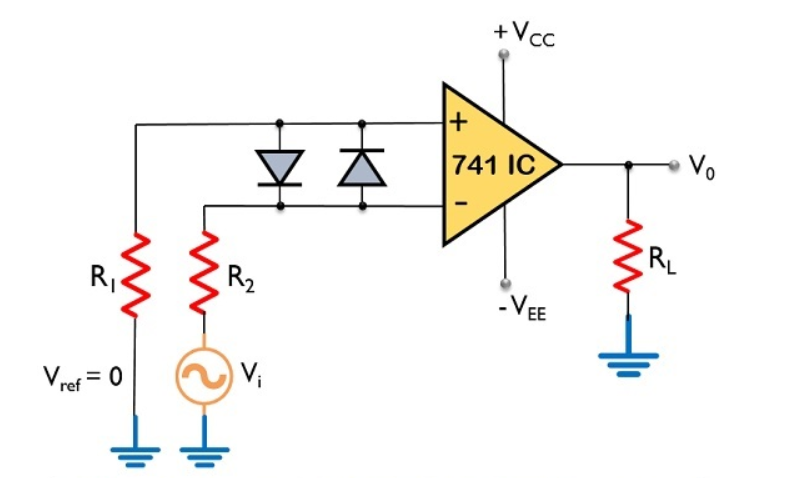
Here, the input signal Vi is provided to the inverting terminal of the op-amp while the non-inverting terminal is grounded by making use of two resistors R1 and R2.
It detects the point where the input signal crosses zero of the reference voltage level. For every crossing, the saturation level of the output signal changes from one to another.
The reference level is set at 0 and applied at the non-inverting terminal of the op-amp. The sine wave applied at the inverting terminal of the op-amp is compared with the reference level each time the phase of the wave changes either from positive to negative or negative to positive.
Firstly, when positive half of the sinusoidal signal appears at the input. Then the op-amp comparator compares the reference voltage level with the peak level of the applied signal.
Vo = Vref – Vi ---------------------------------------(1)
And we know the reference level is 0, thus
Vo = 0 – ( + Vsat) ----------------------------------------(2)
Therefore, Vo = - Vsat ---------------------------------(3)
During the negative half of the signal, thus the peak will have a negative polarity.
Again
Vo = Vref – Vi ---------------------------------------------(4)
Thus,
Vo = 0 - ( - Vsat) --------------------------------------------------(5)
So, we get
Vo = + Vsat ---------------------------------------------(6)
In this way, the zero -crossing detector detects the change in the level of the applied signal.
Zero crossing detector is also known to be a square wave generator. As the output of the window comparator is nothing but a square wave.
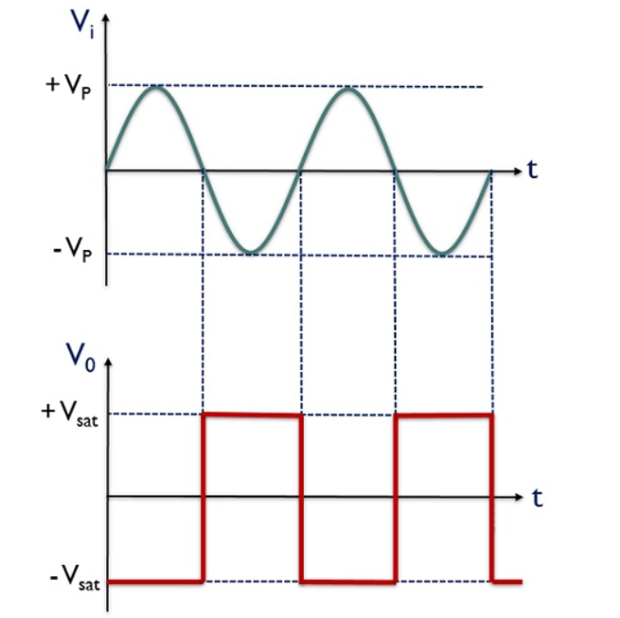
V0 for the positive half of the applied signal is – Vsat,
This is the reason why we have achieved negative half of the square wave at the output when positive half of the sinusoidal signal is applied. While V0 for the negative half of the sinusoidal signal is + Vsat,
Q4) Explain square wave generator?
A4)
Square wave generator
The square wave generator is based on a uA741 opamp (IC1). Resistor R1 and capacitor C1 determines the frequency of the square wave. Resistor R2 and R3 forms a voltage divider setup which feedbacks a fixed fraction of the output to the non-inverting input of the IC.
- Initially, when power is not applied the voltage across the capacitor C1 is 0. When the power supply is switched ON, the C1 starts charging through the resistor R1 and the output of the op-amp will be high.
- A fraction of this high voltage is fed back to the non- inverting pin by the resistor network R2, R3. When the voltage across the charging capacitor is increased to a point the voltage at the inverting pin is higher than the non-inverting pin, the output of the op-amp swings to negative saturation (-Vcc).
- The capacitor quickly discharges through R1 and starts charging in the negative direction again through R1.
- Fraction of the negative high output (-Vcc) is fed back to the non-inverting pin by the feedback network R2, R3. When the voltage across the capacitor has become so negative that the voltage at the inverting pin is less than the voltage at the non-inverting pin, the output of the op-amp swings back to the positive saturation.
- Now the capacitor discharges trough R1 and starts charging in positive direction. This cycle is repeated over time and the result is a square wave swinging between +Vcc and -Vcc at the output of the op-amp.
If the values of R2 and R3 are made equal, then the frequency of the square wave can be expressed using the following equation
F = 1/(2.1976 R1C1)
Q5) Explain triangular wave generator?
A5)
The op-amp IC used in this stage is also uA741 (IC2). Resistor R5 in conjunction with R4 sets the gain of the integrator and resistor R5 in conjunction with C2 sets the bandwidth. The square wave signal is applied to the inverting input of the op-amp through the input resistor R4. The op-amp integrator part of the circuit is shown in the figure below.
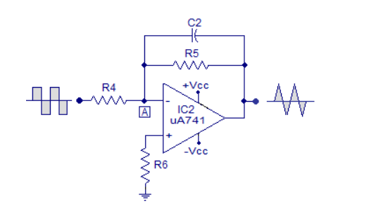
After this initial “kick” the capacitor starts charging and it creates an opposition to the input current flowing through the input resistor R4. The negative feedback compels the op-amp to produce a voltage at its out so that it maintains the virtual ground at the inverting input.
Since the capacitor is charging its impedance Xc keeps increasing and the gain Xc2/R4 also keeps increasing. This results in a ramp at the output of the op-amp that increases in a rate proportional to the RC time constant (T=R4C2) and this ramp increases in amplitude until the capacitor is fully charged.
When the input to the integrator (square wave) falls to the negative peak the capacitor quickly discharges through the input resistor R4 and starts charging in the opposite polarity.
Now the conditions are reversed, and the output of the op-amp will be a ramp that is going to the negative side at a rate proportional to the R4R2 time constant. This cycle is repeated, and the result will be a triangular waveform at the output of the op-amp integrator.
Q6) Explain precision rectifier?
A6)
A rectifier is a circuit that converts alternating current (AC) to Direct current (DC). An alternating current always changes its direction over time, but the direct current flows continuously in one direction.
In a typical rectifier circuit, we use diodes to rectify AC to DC. But this rectification method can only be used if the input voltage to the circuit is greater than the forward voltage of the diode which is typically 0.7V.
The precision rectifier is another rectifier that converts AC to DC, but in a precision rectifier we use an op-amp to compensate for the voltage drop across the diode, that is why we are not losing the 0.6V or 0.7V voltage drop across the diode, also the circuit can be constructed to have some gain at the output of the amplifier as well.
Q7) Explain half-wave precision rectifier?
A7)
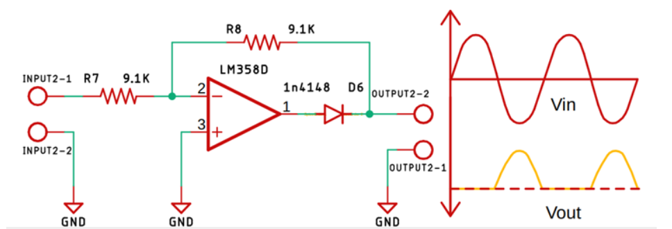
Fig. Half wave precision rectifier circuit
The input and output waveform of the precision rectifier circuit, which is exactly equal to the input. That's because we are taking the feedback from the output of the diode and the op-amp compensates for any voltage drop across the diode. So, the diode behaves like an ideal diode.
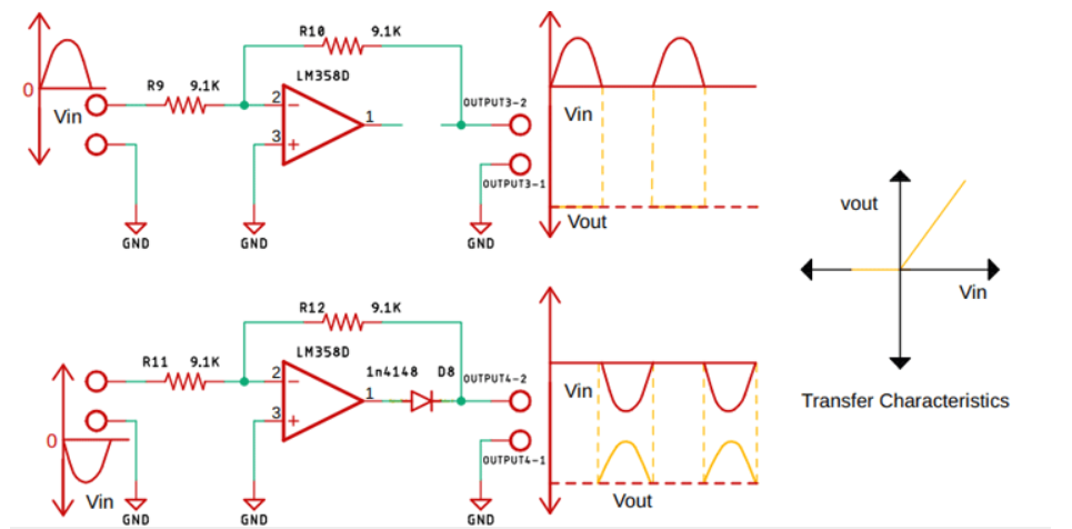
Fig. When positive and negative half cycle of input signal is applied to Op-amp
Q8) Explain peak detector?
A8)
Peak detector circuits are used to determine the peak (maximum) value of an input signal. It stores the peak value of input voltages for infinite time duration until it comes to reset condition.
The peak detector circuit utilizes its property of following the highest value of an input signal and storing it.
Rectifier circuits usually provide an output in proportion to the average value of the input. However, some application requires measurement of the peak value of the signal. Thus, peak detectors are used. Usually, the peak of non-sinusoidal waveforms is measured using a peak detector.
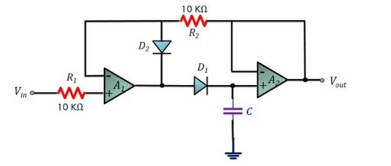
The peak of the input waveform is followed and stored in terms of voltage in the capacitor. If the circuit detects a higher peak, the new peak value is stored in the capacitor until it is discharged.
The capacitor employed in the circuit is charged through the diode by the applied input signal. The small voltage drop across the diode is ignored and the capacitor is charged up to the highest peak of the applied input signal.
Let us consider initially the capacitor is charged to voltage Vc. The diode employed in the circuit gets forward biased when the applied input voltage Vin exceeds the capacitor voltage Vc. Thereby allowing the circuit to behave as a voltage follower. The output voltage follows the applied input voltage until Vin is more than Vc.
As the input voltage Vin reduces below the value of capacitive voltage Vc, it causes the diode to get reverse biased. In such condition, the capacitor retains the value until the input again exceeds the value stored in the capacitor.
Q9) What is monoshot?
A9)
A monostable multivibrator has a “stable” state (say, Vo = 0 V) and a “transient” state (say, Vo = Vhigh). Consider the circuit to be in the stable state in the beginning.
When a certain “event” occurs, it enters the transient state, remains in that state for a time interval T, and then returns to its stable state.
Fig. (a) shows an implementation of the monostable multivibrator circuit using the Schmitt trigger of Figure.
Assume that the circuit is in the stable state in the beginning the capacitor has charged to +V ′ − (−V ′ ) = 2V ′ , the input voltage V− for the Schmitt trigger (with respect to ground) is Vo = −Vm (with Vm = VZ + Von).
And V+ = −Vm R1 R1 + R2 see Figs. (c) and (d). At t = t1, capacitor discharges and VC becomes 0 V, V− changes to −V ′, and the output Vo to +Vm.
When the capacitor starts charging since the input current of the op amp is negligibly small, the charging process can be described by
V−(t) = A e−(t−t1)/τ + B, for t > t1 , where τ = RC.
Using V−(t1) = −V ′ and V (∞) = +V ′, we get A = −2V ′ , B = V ′ ,
i.e., V−(t) = V ′ (1 − 2e −(t−t1)/τ ).
When V− crosses VT H, the output changes to +Vm (at t = t1 + T in Fig. (c).
The capacitor continues to charge, and in about five-time constants, we have once again the original stable state that we started with at t = 0.
To calculate T, we simply substitute V−(t1 + T) = VT H in Eq. and obtain
VT H = V ′ (1 − 2 e −T /τ ) → T = RC × log (2 V ′ /V ′ − VT H ).
Q10) Explain full wave precision rectifier?
A10)
Full wave precision rectifier circuit
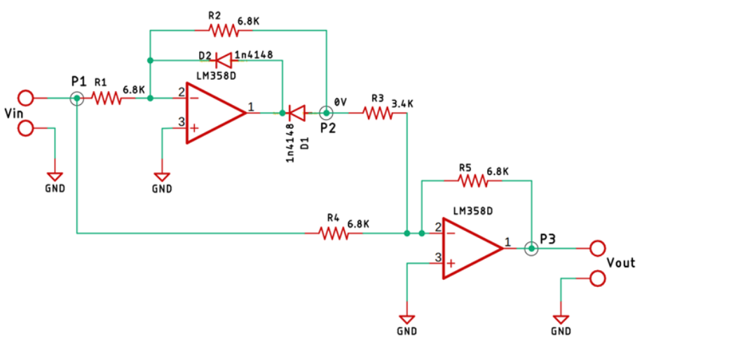
In full wave summing amplifier is added at the output . From the point, P1 to point P2 is the basic precision rectifier circuit and the diode is so configured that we get a negative voltage at the output.
From the point, P2 to point P3 is the summing amplifier, the output from the precision rectifier is fed to the summing amplifier through the resistor R3.
The input from the point P1 is also fed to the summing amplifier with the help of the resistor R4, the resistors R4 and R5 are responsible for setting the gain of the op-amp to 1X.
Since the output from the Point P2 is fed directly to the summing amplifier with the gain of 2X, that means the output voltage will be 2-times the input voltage.
The output is obtained at P3.