Unit - 2
Thyristor Rectifiers
Q1) Draw and explain single phase half wave rectifier with waveform.
A1) Single Phase Half Wave Controlled Rectifier, as the name suggests, is a rectifier circuit which converts AC input into DC output only for positive half cycle of the AC input supply. The word “controlled” means that, we can change the starting point of load current by controlling the firing angle of SCR. Firing of SCR simply means, the SCR turn ON at certain point of time when it is forward biased.
A simple circuit diagram of Single Phase Half Wave Controlled Rectifier is shown in figure below.
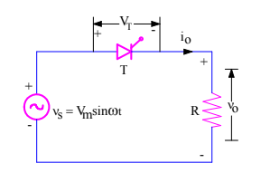
v0 = Load output voltage
i0 = Load current
VT = Voltage across the thyristor T
Following points must be consider for designing controlled rectifier:
a) The important condition is, an SCR will only get turned ON when it is forward biased and fired or gated.
b)SCR will only turn off when current through it reaches below holding current and reverse voltage is applied for a time period more than the SCR turn off time.
Let us assume that thyristor T is fired at a firing angle of α. When wt = α, gate signal will be applied and SCR will start conducting. Refer the following figure.
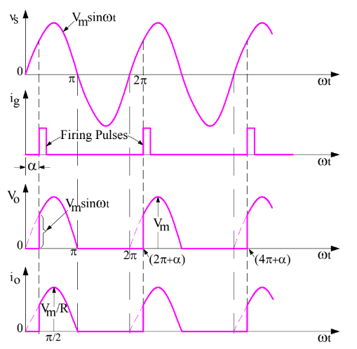
Thyristor T is forward biased for the positive half cycle of supply voltage. The load output voltage is zero till SCR is fired. Once SCR is fired at an angle of α, SCR starts conducting. But as soon as the supply voltage becomes zero at ωt = π, the load current will become zero and after ωt = π, SCR is reversed biased. Thus thyristor T will turn off at ωt = π and will remain in OFF condition till it is fired again at ωt = (2π+α).
A firing angle is defined as,” the angle measured from the instant that gives the largest average output voltage to the instant it is triggered”. As shown in fig, the SCR is fired at ωt =0, 2π, 4 π,etc, the average load (output) voltage is highest so the firing angle should be measured at this instants.
A single phase half wave circuit is one which produces only one pulse of load current during one cycle of source voltage.
Q2) Derive performance parameters for single phase half wave rectifier.
A2) Average voltage V0 across load R for single phase half wave circuit in terms of firing angle α is given by

The maximum value of V0 occurs at α=00,

Average load current ,
For some different types of loads such as electric heater and incandescent lamp, the rms value of load voltage and load current is given as


Power delivered to resistive load = (rms load voltage)* ( rms load current)

Input volt-amperes = (rms source voltage)* (total rms line current)

Input power factor 

Q3) Explain single phase full eave converter with output voltage and current waveforms.
A3) The disadvantages of single phase half wave rectifier or single phase one pulse converter is minimised by single phase full wave or single phase two pulse converters. There are two basic configurations for full wave controlled converters, a) Mid- point converter (uses an input transformer with two windings for each input phase windings) b) A three phase 6 pulse mid- point converters.
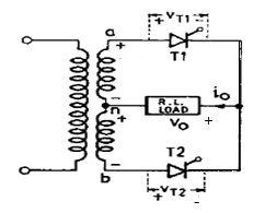
Here SCR T1 and T2 are forward biased during positive and negative half cycles of supply. Suppose T2 is already conducting, after ωt =0, Van is positive, therefore T1 is forward biased, and when fires at α, T1 gets turned ON. At this firing angle α, supply voltage vs =2Vm Sin α , reverse biases T2 which turns OFF T2. Here T1 is called incoming thyristor (SCR) and T2 is outgoing thyristor. When T1 is forward biased, T2 is reversed biased, so load current is also transferred from T2 to T1. This process of turned OFF of SCR (T2) by natural reversible ac supply voltage is called natural commutation or Line commutation.
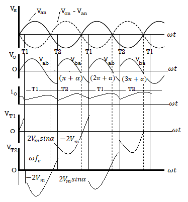
Fig: voltage and current waveforms of single phase full wave converter
The following observation can be made from diagram
(a) For commutation of SCR (T2)) need to be done, the incoming SCR (T1) must be forward biased and T2 should be reversed biased.
(b) When incoming SCR (T1) is turned ON, current is transferred from outgoing SCR (T2) to Incoming SCR (T1).
(c) The circuit turn-OFF time must be greater than SCR turn-OFF time.
Q4) Draw and explain single phase full bridge converter with RLE load with waveforms.
A4)
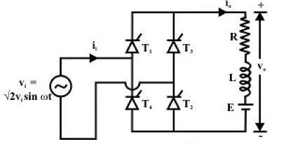
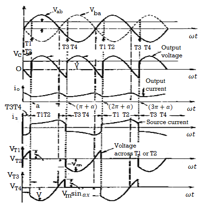
Fig (a) shows the circuit diagram of a single phase fully controlled bridge converter. The single phase fully controlled bridge converter is designed by replacing all the diode of the corresponding uncontrolled converter by thyristors. Thyristors T1 and T2 are fired together while T3 and T4 are fired 180º after T1 and T2. From the circuit diagram, it is clear that for any load current to flow at least one thyristor from the top group (T1, T3) and one thyristor from the bottom group (T2, T4) must conduct. It can also be noted that neither T1T3 nor T2T4 can conduct simultaneously. For example whenever T3 and T4 are in the forward blocking state and a gate pulse is applied to them, they turn ON and at the same time a negative voltage is applied across T1 and T2 commutating them immediately. Similar for T1 and T2. For the same reason T1T4 or T2T3 cannot conduct simultaneously.
Therefore, the only possible conduction modes when the current i0 can flow are T1T2 and T3T4. It is possible that at a given point no one of the thyristors conduct. This situation will typically occur when the load current becomes zero in between the firings of T1T2 and T3T4. Once the load current becomes zero all thyristors remain off. In this mode the load current remains zero. Consequently the converter is said to be operating in the discontinuous conduction mode. It is to be noted that whenever T1 and T2 conducts, the voltage across T3 and T4 becomes –Vi. Therefore T3 and T4 can be fired only when Vi is negative i.e, over the negative half cycle of the input supply voltage. Similarly T1 and T2 can be fired only over the positive half cycle of the input supply. The voltage across the devices when none of the thyristors conduct depends on the off state impedance of each device. Under normal operating condition of the converter the load current may or may not remain zero over some interval of the input voltage cycle. If i0 is always greater than zero then the converter is said to be operating in the continuous conduction mode. In this mode of operation of the converter T1T2 and T3T4 conducts for alternate half cycle of the input supply. However, in the discontinuous conduction mode none of the thyristors conduct over some portion of the input cycle. The load current remains zero during that period.
Q5) Explain 3-phase full wave bridge converter in detail.
A5)
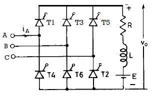
Fig(a): power circuit for 3-phase bridge converter
The 3-phase input supply is connected to terminals A, B, C and the load RLE is connected across the output terminals. This circuit works as 3-phase converter for firing angle delay 00<α ≤ 900 . A 3-phase is preferred where regeneration of power is required. The numbering of SCR’s shown in fig is 1, 3, 5 for positive group and 2, 4, 6 for negative group.
For α= 00 , T1, T2,..T6 behaves like a diodes. This is shown in waveform below in fig(b). Note that for α= 00, T1 is triggered at wt= π/6, T2 at 900, T3 at 1500, and so on. The load voltage waveform is shown in (c).
For α= 600, the conduction sequence of SCR’s T1 to T6 is shown in below fig(d). Here T1 is triggered at wt=300+600=900, T2 at 900+600=1500 and so on. Note that each SCR conducts for 1200 , when T1 is triggered, T5 is turned OFF and T1is turned ON. T6 is already conducting. As T1 is connected to terminal A and T6 is connected to B, the voltage vab appears across load and it varies from 1.5Vm to zero. H ere Vmp is a maximum phase voltage.
When T2 is turned ON, T6 is commutated from negative group and T1 is already conducting. As T1 and T2 are connected to terminal A and C, the voltage vac appears across load. The same sequence is continued for other SCRs.
As both group of SCR’s are fired at an interval of 600, this means that commutation occurs every 600, alternatively in upper and lower group of SCR’s. At any time, two SCR’s, one from positive group and other from negative group, must conduct together for source to energise that load. For ABC phase sequence of 3-phase supply, SCR’s conducts in pairs; T1and T2, T2 and T3 and so on.
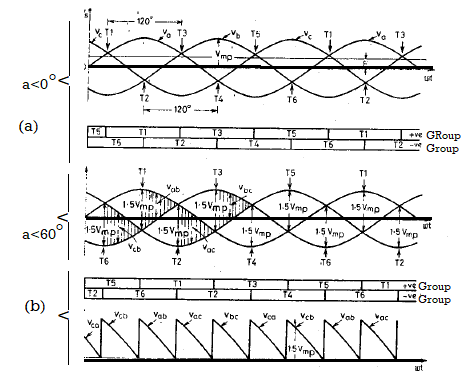
Fig: voltage waveform and conduction of SCR’s in 3-phase converter.
Q6) Derive the expression for average output voltage and source current of 3-phase full wave bridge converter.
A6)
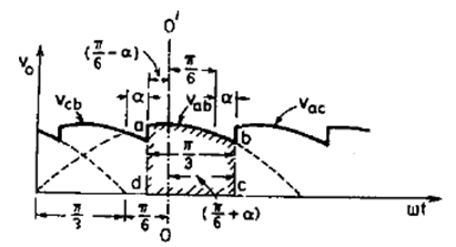
Fig: Output voltage waveform for 3-phase full converter
The average output voltage V0 can be obtained from above output voltage waveform. Note that periodicity of output voltage is π/3 radians. Average value of output voltage is obtained by finding the dashed area abcd over a periodic cycle and then dividing it by the periodic time.
With OO’ as the origin at the maximum value of vab, V0 is given by,


Here, Vm is maximum line voltage.
If sine function is used for the source voltage, then vab= Vm sin wt because vab= 0 at wt=0.


It is observed from fig(b) that source current for phase A i.e. iA(or for any other phase) flows for 1200 for every 1800.therefore in case of output current is assumed at I0, the rms value of source current is

Q7) A three phase fully controlled bridge converter operating from a 3 phase 220 V, 50 Hz supply is used to charge a battery bank with nominal voltage of 240 V. The battery bank has an internal resistance of 0.01 Ω and the battery bank voltage varies by ± 10% around its nominal value between fully charged and uncharged condition. Assuming continuous conduction find out.
(i) The range of firing angle of the converter.
(ii) The range of ac input power factor.
(iii) The range of charging efficiency.
When the battery bank is charged with a constant average charging current of 100 Amps through a 250 mH lossless inductor.
A7)
The maximum and minimum battery voltages are, VB Min = 0.9 × VB Nom = 216 volts and VB Max = 1.1 × VB Nom = 264 volts respectively.
Since the average charging current is constant at 100 A.
V0 Max = VB Max + 100 × RB = 264 + 100 × 0.01 = 265 volts
V0 Min = VB Min + 100 × RB = 216 + 100 × 0.01 = 217 volts.
(i) But 0 MaxLMin32V=V cos απ ∴ α Min = 26.88º
0 MinLMax32V=V cos απ ∴ α Max = 43.08º
(ii) Input power factor is maximum at minimum α and vice versa
∴Maxmin3p.f. Max = Distortion factor Displacement factor=×cos α=0.85π×Max3p.f. Min = ×cos α=0.697π
(iii) Power loss during charging = 20RMsBI R
But 22220RMs012II+I+I+........= and 22AKBKKKV+VVI=6KωL62KωL≈
For α = α Min
VA1 = 0.439 V, VB1 = 48.48 V, I1 = 0.073 Amps
VA2 = 10.76, VB2 = 20.15 V, I2 = 0.017 Amps.
∴ 22220RMsJ100+(0.073)+(0.017)=10000.00562≈
∴ Ploss = 100 watts.
At α Min, P0 = I0 × VB Max = 26400 watts.
∴ Charging efficiency = 2640026400 + 100 = 99.6%
Similarly for α Max, 220RMs0I ≈
∴ Ploss = 100 watts
P0 = I0 × VB Min = 21600 watts.
∴ Charging efficiency = 2160021600 + 100 = 99.54%
Q8) A three phase fully controlled converter operates from a 3 phase 230 V, 50 Hz supply through a Y/Δ transformer to supply a 220 V, 600 rpm, 500 A separately excited dc motor. The motor has an armature resistance of 0.02 Ω. What should be the transformer turns ratio such that the converter produces rated motor terminal voltage at 0º firing angle. Assume continuous conduction. The same converter is now used to brake the motor regeneratively in the reverse direction. If the thyristors are to be provided with a minimum turn off time of 100 μs, what is the maximum reverse speed at which rated braking torque can be produced.
A8) From the given question
L32V=220π ∴ VL = 162.9 V
Where VL is the secondary side line and also the phase voltage since the secondary side is Δ connected. Primary side phase voltage = 230V3 = 132.79 V
∴ Turns ratio = 132.791:1.2267162.9=.
During regenerative braking in the reverse direction the converter operates in the inverting mode.
Mintq=100μS ∴ oMinMinβ=ωtq=1.8
∴ α Max = 180 – β Min = 178.2º
∴ Maximum negative voltage that can be generated by the converter is
OL32V cos 178.2=- 219.89 Vπ
For rated braking torque Ia = 500 A
∴ Eb = Va – Iara = - 229.89 V.
At 600 RPM Eb = 220 – 500 × 0.02 = 210 V.
∴ Max reverse speed is 229.89×600=656.83 RPM210.
Q9) A single phase fully controlled bridge converter operates in the continuous conduction mode from a 230V, 50HZ single phase supply with a firing angle α = 30°. The load resistance and inductances are 10Ω and 50mH respectively. Find out the 6th harmonic load current as a percentage of the average load current.
A9)
The average dc output voltage is

Average output load current=
From equation (10.18)
From equation (10.19)


Q10) A single phase full wave ac voltage controller working on ON-OFF control technique has supply voltage of 230V, RMS 50Hz, load = 50Ω. The controller is ON for 30 cycles and off for 40 cycles.
Calculate
1) ON & OFF time intervals.
2) RMS output voltage
3) Input P.F.
4) Average and RMS thyristor currents
A10)


N=number of input cycles during which controller is ON; n=30
M=number of input cycles during which controller is OFF; m=40


Duty cycle 
RMS output voltage


Input Power Factor P.F.=

PF=0.654653
Average Thyristor Current Rating

Where


RMS Current Rating Thyristor

