Unit - 1
Introduction
Q1) Design a CMOS digital circuit that realizes the Boolean function 
A1)
Step1:
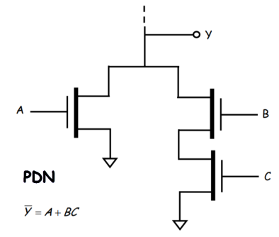
Design the PDN
First, we must rewrite the Boolean function as:
 =f(a, b, c)
In other words, write the complemented output in terms of un-complemented inputs
We must first complement this equation, and then apply DeMorgan’s Theorem


We can thus realize this logic with the following NMOS PDN
Step2: Design the PUN
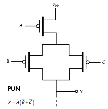
First, we must rewrite the Boolean function as Y =f( ,
,  ,
,  )
)
In other words, write the un-complemented output in terms of complemented inputs.
Again, using DeMorgan’s Theorem


We can thus realize this logic with the following PMOS PUN
The complete CMOS design circuit will be
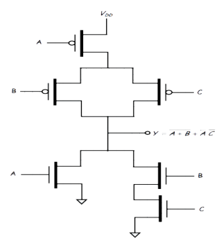
Q2) Design a gate that realizes this Boolean algebraic expression 
A2)
Step 1: Design PDN
First write Boolean Expression as


Thus, Y’= AB+C’
Therefore, the inputs to this logic gate should be A, B, and C’ (i.e., A, B, and the complement of C). Note that this Boolean expression “says” that: “The output is low if either, A AND B are both high, OR C’ is high” Of course another way of “saying” this is: “The output is low if either A AND B are both high, OR C is low” The PDN is therefore:
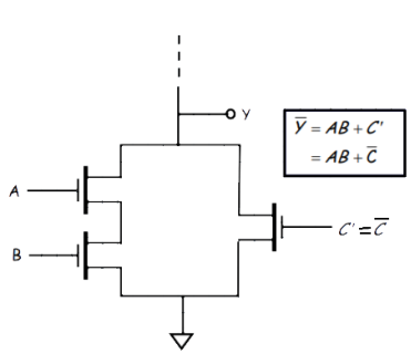
Step 2: Design the PUN
Note we have as similar problem as before—the expression for Y cannot explicitly be written in terms of complemented inputs A’ B’ and C’
Y= (A’+B’) C
“The output will be high if, either A OR B are low, AND C’ is low” Which is equivalent to saying: “The output will be high if, either A OR B are low, AND C is high” The CMOS digital logic device is therefore
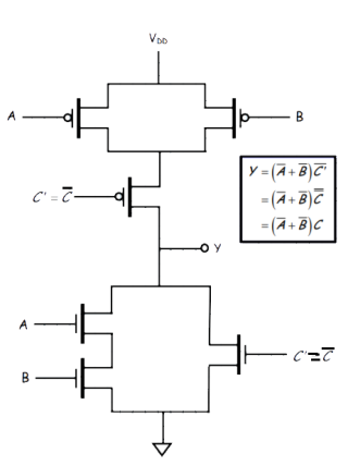
Q3) Draw the minimum CMOS transistor network that implements the functionality of Boolean equation F= ((A+B) C + D)'.
A3)
Using the above steps to realise the given Boolean function complete CMOS design we get is
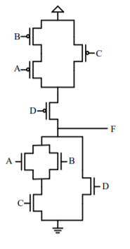
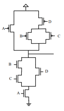
Q4) Draw the minimum CMOS transistor network that implements the functionality of Boolean equation F= (A (B C + D))'.
A4)
Using the above steps to realise the given Boolean function complete CMOS design we get is
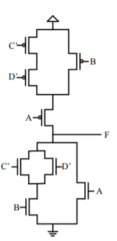
Q5) Draw the minimum CMOS transistor network that implements the functionality of Boolean equation F= (A + (B' + CD)')'.
A5) F= (A + (B' + CD)')' = (A + B(CD)')' = (A + B (C' + D'))'
Using the above steps to realise the given Boolean function complete CMOS design we get is
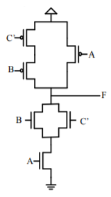
Q6) Draw the minimum CMOS transistor network that implements the functionality of Boolean equation F= (A' + B'C).
A6) F = (A' + B'C) = ((A' + B'C)')'= (A (B'C)')' = (A (B + C'))'
Using the above steps to realise the given Boolean function complete CMOS design we get is
Q7) How to implement F = ab + bc + ca?
A7)

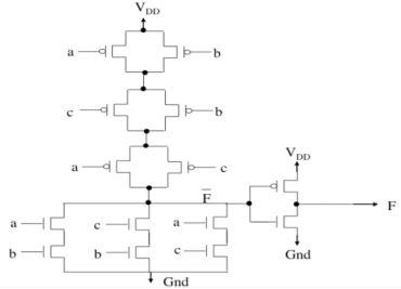
The above circuit shows the implementation.
Q8) Explain the difference between Latch and Flip Flop?
A8)
Latch | Flip-flop |
Latches are transparent devices i.e., when they are enabled, the output changes immediately if the input changes. | A transition from low to high or high to low of the clock signal will cause the flip-flop to either change its output or retain it depending on the input signal. |
A latch is a level Sensitive device (Level Triggering is involved). | A flip-flop is an edge sensitive device (Edge Triggering is involved). |
Latches are simpler to design as there is no clock signal (no careful routing of clock signal is required). | When compare to latches, flip-flops are more complex to design as they have clock signal and it has to be carefully routed. This is because all the flip-flops in a design should have a clock signal and the delay in the clock reaching each flip-flop must be minimum or negligible. |
The operation of a latch is faster as they do not have to wait for any clock signal. | Flip-flops are comparatively slower than latches due to clock signal. |
The power requirement of a latch is less. | Power requirement of a flip-flop is more. |
A Latch works based on the enable signal | A flip-flop works based on the clock signal |
Q9) Explain the CMOS logic basic structure?
A9)
The MOSFET (metal-oxide-semiconductor field-effect transistor) are of two types: PMOS (p-type MOS) and NMOS (n-type MOS).
A new type of MOSFET logic is made combining both the PMOS and NMOS processes and is called as complementary MOS (CMOS).
CMOS stands for “Complementary Metal Oxide Semiconductor”.
It is one of the most popular technology in the chip design industry and is used today to form integrated circuits for various applications.
Computer memories, CPUs and cell phones make use of this technology due to various advantages. This technology uses both P and N channel semiconductor devices.
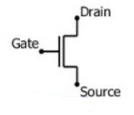
NMOS
NMOS is built on a p-type substrate with n-type source and drain diffused on it. Here, the majority carriers are electrons. When a high voltage is applied to the gate, the NMOS conducts and when low voltage is applied to the gate, it does not conduct. NMOS is faster than PMOS, as the carriers are electrons that travel twice as fast as the holes.
PMOS
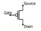
P-MOS consists of P-type Source and Drain diffused on an N-type substrate. Here, majority carriers are holes. When a high voltage is applied to the gate, the PMOS does not conduct and when a low voltage is applied, it conducts. These devices are more immune to noise than NMOS devices.
CMOS Applications
- Computer memories, CPUs
- Microprocessor designs
- Flash memory chip designing
- Used to design application specific integrated circuits (ASICs)
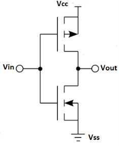
Fig: CMOS
The inverter circuit as shown in the figure above. It consists of PMOS and NMOS FET. The input A serves as the gate voltage for both transistors.
The NMOS transistor has an input from Vss (ground) and PMOS transistor has an input from Vdd. The terminal Y is output. When a high voltage (~ Vdd) is given at input terminal (A) of the inverter, the PMOS becomes open circuit and NMOS switched OFF so the output will be pulled down to Vss.
When a low-level voltage (<Vdd, ~0v) applied to the inverter, the NMOS switched OFF and PMOS switched ON. So, the output becomes Vdd or the circuit is pulled up to Vdd.
INPUT | LOGIC INPUT | OUTPUT | LOGIC OUTPUT |
0 V | 0 | Vdd | 1 |
Vdd | 1 | 0 v | 0 |
Q10) Draw and explain CMOS realization of Inverter and AND gate?
A10) Inverter
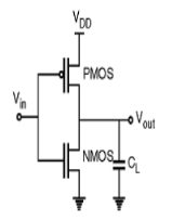
Fig: CMOS inverter
- It consists of PMOS and NMOS FET.
- The input A serves as the gate voltage for both transistors.
- The NMOS transistor has an input from Vss (ground) and PMOS transistor has an input from Vdd. The terminal Y is output.
- When a high voltage (~ Vdd) is given at input terminal (A) of the inverter, the PMOS becomes open circuit and NMOS switched OFF so the output will be pulled down to Vss.
- The truth table of inverter is:
A | Y = A’ |
0 | 1 |
1 | 0 |

Fig: NOT gate
AND Gate
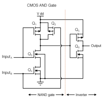
As with the TTL NAND gate, the CMOS NAND gate circuit may be used as the starting point for the creation of an AND gate. All that needs to be added is another stage of transistors to invert the output signal.
Q11) Draw and explain CMOS realization of NOR and NAND gate?
A11) NAND Gate
As with the TTL NAND gate, the CMOS NAND gate circuit may be used as the starting point for the creation of an AND gate. All that needs to be added is another stage of transistors to invert the output signal.
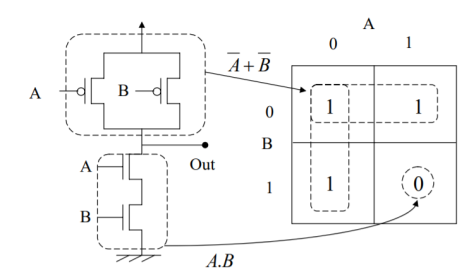
PDN connected to GND: 
PUN connected to 
NOR Gate
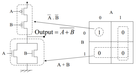
A CMOS NOR gate circuit uses four MOSFETs just like the NAND gate, except that its transistors are differently arranged. Instead of two paralleled sourcing (upper) transistors connected to Vdd and two series-connected sinking (lower) transistors connected to ground, the NOR gate uses two series-connected sourcing transistors and two parallel-connected sinking transistors like this
Q12) Explain sequential circuit test?
A12) Sequential circuit test
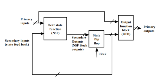
ATPG for sequential circuits
•variations required in fault model, algebra and ATPG procedure
•compare the ATPG Complexity
•A special scheme called “scan chain” which modifies a sequential circuit into a virtual combinational one”.
When a circuit powers up, the flip-flops can have any value (0 or 1).
•ATPG need to control (indirectly) the outputs of flip-flops and observe (indirectly) the inputs to the flip-flops.
•Once achieved, ATPG for these combinational blocks can be done using D algorithm.
•Single clock sequential circuits.
•Each flip-flop is treated as 1-bit memory element with ONE common clock.
•After a clock edge, the secondary output pattern (next state) is transferred to the output of the flip-flops (present state), which become new secondary inputs. Also, the primary outputs are updated. This activity occurs at each clock edge, and so it is called “synchronous” operation.
•Single stuck at faults are assumed in NSF and OFB.
•Internal faults of flip-flops are not modeled; their output and input faults are modeled as faults on input and output signals of the combinational blocks.
•No faults are considered in the clock signal.
•Most of the time, D-flip-flops are used in VLSI designs. So, in this course whenever we refer to a flip-flop we essentially mean a D-flipflop.
Q13) Explain the need of testability?
A13) Need of Design for Testability (DFT)
- DFT is a technique, which facilitates a design to become testable after fabrication. Add on logic is added along with the design logic during implementation process helps in post-production testing.
- Post-production testing is necessary because, the process of manufacturing is not 100% error free.
- There are defects in silicon which contribute towards the errors introduced in the physical device.
- A chip will not work as per the specifications if there are any errors introduced in fabrication.
- All the functional tests run on each of a million physical devices, is very time consuming, there was a need for a method, which assures its maturity without running full exhaustive tests on the physical device in order to ensure that the device has been manufactured correctly.
Q14) What are fabrication techniques explain?
A14) The basic IC fabrication steps will be described in the following sections. Some of these steps may be carried out many times, in different combinations and/or processing conditions during a complete fabrication run.
Silicon Wafers
The starting material for modern integrated circuits is very-high-purity, single-crystal silicon. The material is initially grown as a single crystal ingot. It takes the shape of a steel-gray solid cylinder 10 cm to 30 cm in diameter and can be one to two meters in length. This crystal is then sawed (like a loaf of bread) to produce circular wafers that are 400μm to 600μm thick (a micrometer, or micron, μm, is a millionth of a meter). The surface of the wafer is then polished to a mirror finish using chemical and mechanical polishing (CMP) techniques. Semiconductor manufacturers usually purchase ready-made silicon wafers from a supplier and rarely start their fabrication process in ingot form. The basic electrical and mechanical properties of the wafer depend on the orientation of the crystalline structure, the impurity concentrations, and the type of impurities present. These variables are strictly controlled during crystal growth. A specific amount of impurities can be added to the pure silicon in a process known as doping. This allows the alteration of the electrical properties of the silicon, in particular its resistivity. Depending on the types of impurity, either holes (in p-type silicon) or electrons (in n-type silicon) can be responsible for electrical conduction. If a large number of impurity atoms is added, the silicon will be heavily doped (e.g., concentration > ∼1018 atoms/cm−3). When designating the relative doping concentrations in semiconductor material, it is common to use the + and – symbols. A heavily doped (low-resistivity) n-type silicon wafer is referred to as n+material, while a lightly doped material (e.g., concentration < ∼1016 atoms/cm−3) is referred to as n−. Similarly, p+ and p− designations refer to the heavily doped and lightly doped p-type regions, respectively. The ability to control the type of impurities and the doping concentration in the silicon permits the formation of diodes, transistors, and resistors in integrated circuits.
Oxidation
In oxidation, silicon reacts with oxygen to form silicon dioxide (SiO2). To speed up this chemical reaction, it is necessary to carry out the oxidation at high temperatures (e.g., 1000–1200°C) and inside ultraclean furnaces. To avoid the introduction of even small quantities of contaminants (which could significantly alter the electrical properties of the silicon), it is necessary to operate in a clean room. Particle filters are used to ensure that the airflow in the processing area is free from dust. All personnel must protect the clean-room environment by wearing special lint-free clothing that covers a person from head to toe. The oxygen used in the reaction can be introduced either as a high-purity gas (referred to as a “dry oxidation”) or as steam (forming a “wet oxidation”). In general, wet oxidation has a faster growth rate, but dry oxidation gives better electrical characteristics. The thermally grown oxide layer has excellent electrical insulation properties. The dielectric strength for SiO2 is approximately 107 V/cm. It has a dielectric constant of about 3.9, and it can be used to form excellent MOS capacitors. Silicon dioxide can also serve as an effective mask against many impurities, allowing the introduction of dopants into the silicon only in regions that are not covered with oxide. Silicon dioxide is a transparent film, and the silicon surface is highly reflective. If white light is shone on an oxidized wafer, constructive and destructive interference will cause certain colors to be reflected. The wavelengths of the reflected light depend on the thickness of the oxide layer. In fact, by categorizing the color of the wafer surface, one can deduce the thickness of the oxide layer. The same principle is used by more sophisticated optical inferometers to measure film thickness. On a processed wafer, there will be regions with different oxide thicknesses. The colors can be quite vivid and are immediately obvious when a finished wafer is viewed with the naked eye.
Photolithography
Mass production with economy of scale is the primary reason for the tremendous impact VLSI has had on our society. The surface patterns of the various integrated-circuit components can be defined repeatedly using photolithography. The sequence of photolithographic steps is as illustrated in Fig. Below. The wafer surface is coated with a photosensitive layer called photoresist, using a spin-on technique. After this, a photographic plate with drawn patterns (e.g., a quartz plate with chromium layer for patterning) will be used to selectively expose the photoresist under a deep ultraviolet illumination (UV). The exposed areas will become softened (for positive photoresist). The exposed layer can then be removed using a chemical developer, causing the mask pattern to be duplicated on the wafer. Very fine surface geometries can be reproduced accurately by this technique. Furthermore, the patterns can be projected directly onto the wafer, or by using a separate photomask produced by a 10x “step and repeat” reduction technique as shown in Fig. Below. The patterned photoresist layer can be used as an effective masking layer to protect materials below from wet chemical etching or reactive ion etching (RIE). Silicon dioxide, silicon nitride, polysilicon, and metal layers can be selectively removed using the appropriate etching methods (see next section). After the etching step(s), the photoresist is stripped away, leaving behind a permanent pattern of the photomask on the wafer surface. To make this process even more challenging, multiple masking layers (which can number more than 20 in advanced VLSI fabrication processes) must be aligned precisely on top of previous layers. This must be done with even finer precision than the minimum geometry size of the masking patterns. This requirement imposes very critical mechanical and optical constraints on the photolithography equipment.
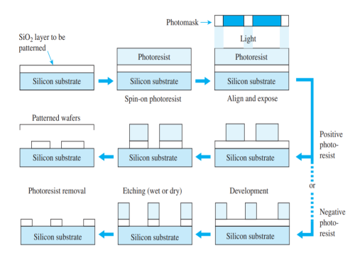
Fig: Photolithography using positive or negative photoresist.
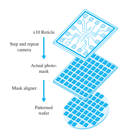
Fig: Conceptual illustration of a step-and-repeat reduction technique to facilitate the mass production of integrated circuits.
Etching
To permanently imprint the photographic patterns onto the wafer, chemical (wet) etching or RIE dry etching procedures can be used. Chemical etching is usually referred to as wet etching. Different chemical solutions can be used to remove different layers. For example, hydrofluoric (HF) acid can be used to etch SiO2, potassium hydroxide (KOH) for silicon, phosphoric acid for aluminium, and so on. In wet etching, the chemical usually attacks the exposed regions that are not protected by the photoresist layer in all directions (isotropic etching). Depending on the thickness of the layer to be etched, a certain amount of undercut will occur. Therefore, the dimension of the actual pattern will differ slightly from the original pattern. If exact dimension is critical, RIE dry etching can be used. This method is essentially a directional bombardment of the exposed surface using a corrosive gas (or ions). The cross section of the etched layer is usually highly directional (anisotropic etching) and has the same dimension as the photoresist pattern.
Diffusion
Diffusion is a process by which atoms move from a high-concentration region to a low concentration region. This is very much like a drop of ink dispersing through a glass of water except that it occurs much more slowly in solids. In VLSI fabrication, this is a method to introduce impurity atoms (dopants) into silicon to change its resistivity. The rate at which dopants diffuse in silicon is a strong function of temperature. Diffusion of impurities is usually carried out at high temperatures (1000–1200°C) to obtain the desired doping profile. When the wafer is cooled to room temperature, the impurities are essentially “frozen” in position.

Fig: (a) Cross-sectional view of an isotropic oxide etch with severe undercut beneath the photoresist layer. (b) Anisotropic etching, which usually produces a cross section with no undercut.
The diffusion process is performed in furnaces similar to those used for oxidation. The depth to which the impurities diffuse depends on both the temperature and the processing time. The most common impurities used as dopants are boron, phosphorus, and arsenic. Boron is a p-type dopant, while phosphorus and arsenic are n-type dopants. These dopants can be effectively masked by thin silicon dioxide layers. By diffusing boron into an n-type substrate, a pn junction is formed (diode). If the doping concentration is heavy, the diffused layer can also be used as a conducting layer with very low resistivity.
Ion Implantation
Ion implantation is another method used to introduce impurities into the semiconductor crystal. An ion implanter produces ions of the desired dopant, accelerates them by an electric field, and allows them to strike the semiconductor surface. The ions become embedded in the crystal lattice. The depth of penetration is related to the energy of the ion beam, which can be controlled by the accelerating-field voltage. The quantity of ions implanted can be controlled by varying the beam current (flow of ions). Since both voltage and current can be accurately measured and controlled, ion implantation results in impurity profiles that are much more accurate and reproducible than can be obtained by diffusion. In addition, ion implantation can be performed at room temperature. Ion implantation normally is used when accurate control of the doping profile is essential for device operation.
Chemical Vapor Deposition
Chemical vapor deposition (CVD) is a process by which gases or vapors are chemically reacted, leading to the formation of solids on a substrate. CVD can be used to deposit various materials on a silicon substrate including SiO2, Si3N4, polysilicon, and so on. For instance, if silane gas and oxygen are allowed to react above a silicon substrate, the end product, silicon dioxide, will be deposited as a solid film on the silicon wafer surface. The properties of the CVD oxide layer are not as good as those of a thermally grown oxide, but they are sufficient to allow the layer to act as an electrical insulator. The advantage of a CVD layer is that the oxide deposits at a faster rate and a lower temperature (below 500°C). If silane gas alone is used, then a silicon layer will be deposited on the wafer. If the reaction temperature is high enough (above 1000°C), the layer deposited will be a crystalline layer (assuming that there is an exposed crystalline silicon substrate). Such a layer is called an epitaxial layer, and the deposition process is referred to as epitaxy instead of CVD. At lower temperatures, or if the substrate surface is not single-crystal silicon, the atoms will not be able to aligned along the same crystalline direction. Such a layer is called polycrystalline silicon (poly Si), since it consists of many small crystals of silicon aligned in random fashion. Polysilicon layers are normally doped very heavily to form highly conductive regions that can be used for electrical interconnections.
Q15) Describe the lambda rule used for circuit design?
A15) The design rules primary address two issues:
1. The geometrical reproduction of features that can be reproduced by the mask making and lithographical process, and
2. The interaction between different layers.
There are primarily two approaches in describing the design rules.
1. Linear scaling is possible only over a limited range of dimensions.
2. Scalable design rules are conservative. This, results in over dimensioned and less dense design.
3. This rule is not used in real life.
1. Scalable Design Rules (e.g., SCMOS, λ-based design rules):
In this approach, all rules are defined in terms of a single parameter λ. The rules are so chosen that a design can be easily ported over a cross section of industrial process, making the layout portable. Scaling can be easily done by simply changing the value of. The key disadvantages of this approach are:
2. Absolute Design Rules (e.g., μ-based design rules): In this approach, the design rules are expressed in absolute dimensions (e.g., 0.75μm) and therefore can exploit the features of a given process to a maximum degree. Here, scaling and porting is more demanding, and has to be performed either manually or using CAD tools. Also, these rules tend to be more complex especially for deep submicron.
The fundamental unity in the definition of a set of design rules is the minimum line width. It stands for the minimum mask dimension that can be safely transferred to the semiconductor material. Even, for the same minimum dimension, design rules tend to differ from company to company, and from process to process. Now, CAD tools allow designs to migrate between compatible processes.
Layer Representations
With increase of complexity in the CMOS processes, the visualization of all the mask levels that are used in the actual fabrication process becomes inhibited. The layer concept translates these masks to a set of conceptual layout levels that are easier to visualize by the circuit designer. From the designer's viewpoint, all CMOS designs have the following entities:
• Two different substrates and/or wells: which is p-type for NMOS and n-type for PMOS.
• Diffusion regions (p+ and n+): which defines the area where transistors can be formed. These regions are also called active areas. Diffusion of an inverse type is needed to implement contacts to the well or to substrate. These, are called select regions.
• Transistor gate electrodes: Polysilicon layer
• Metal interconnect layers
• Interlayer contacts and via layers. The layers for typical CMOS processes are represented in various figures in terms of:
• A color scheme (Mead-Conway colors).
• Other color schemes designed to differentiate CMOS structures.
• Varying stipple patterns
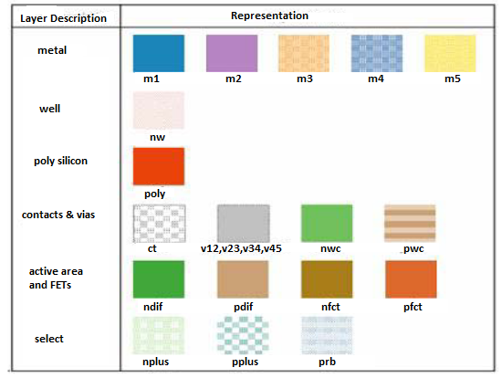
Fig: Mead Conway Colour coding for layers
Q16) What are stick diagram?
A16) Stick Diagrams
Another popular method of symbolic design is "Sticks" layout. In this, the designer draws a freehand sketch of a layout, using coloured lines to represent the various process layers such as diffusion, metal and polysilicon. Where, polysilicon crosses diffusion, transistors are created and where metal wires join diffusion or polysilicon, contacts are formed. This notation indicates only the relative positioning of the various design components. The absolute coordinates of these elements are determined automatically by the editor using a compactor.
The compactor translates the design rules into a set of constraints on the component positions, and solve a constrained optimization problem that attempts to minimize the area or cost function. The advantage of this symbolic approach is that the designer does not have to worry about design rules, because the compactor ensures that the final layout is physically correct. The disadvantage of the symbolic approach is that the outcome of the compaction phase is often unpredictable. The resulting layout can be less dense than what is obtained with the manual approach. In addition, it does not show exact placement, transistor sizes, wire lengths, wire widths, tub boundaries.
For example, stick diagram for CMOS Inverter is shown below
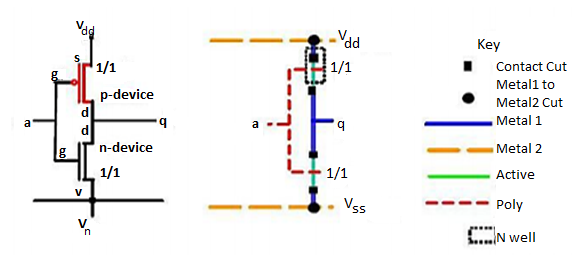
Fig: Stick Diagram of CMOS inverter
Q17) What are Y charts. Mention is use and explain in detail?
A17) The greatest challenge in modern VLSI design is not in designing the individual transistors but rather in managing system complexity. Modern System-On-Chip (SOC) designs combine memories, processors, high speed I/O interfaces, and dedicated application-specific logic on a single chip. They use hundreds of millions (soon billions) of transistors. The implementation must be divided among large teams of engineers and each engineer must be highly productive. If the implementation is too rigidly partitioned, each block can be optimized without regard to its neighbors, leading to poor system results. Conversely, if every task is interdependent with every other task, design will progress too slowly. Design managers face the challenge of choosing a suitable trade-off between these extremes. There is no substitute for practical experience in making these choices, and talented engineers who have experience with multiple designs are very important to the success of a large project.
Digital VLSI design is often partitioned into five interrelated tasks: architecture design, microarchitecture design, logic design, circuit design, and physical design. Architecture describes the functions of the system. For example, the x86 microprocessor architecture specifies the instruction set, register set, and memory model. Microarchitecture describes how the architecture is partitioned into registers and functional units. The 80386, 80486, Pentium, Pentium II, Pentium III, Pentium 4, Celeron, Cyrix MII, AMD K5, and Athlon are all microarchitectures offering different performance / transistor count trade-offs for the x86 architecture. Logic describes how functional units are constructed. For example, various logic designs for a 32-bit adder in the x86 integer unit include ripple carry, carry lookahead, and carry select.
Circuit design describes how transistors are used to implement the logic. For example, a carry lookahead adder can use static CMOS circuits, domino circuits, or pass transistors. The circuits can be tailored to emphasize high performance or low power. Physical design describes the layout of the chip These elements are inherently interdependent. For example, choices of microarchitecture and logic are strongly dependent on the number of transistors that can be placed on the chip, which depends on the physical design and process technology. Similarly, innovative circuit design that reduces a cache access from two cycles to one can influence which microarchitecture is most desirable. The choice of clock frequency depends on a complex interplay of microarchitecture and logic, circuit design, and physical design.
Deeper pipelines allow higher frequencies but lead to greater performance penalties when operations early in the pipeline are dependent on those late in the pipeline. Many functions have various logic and circuit designs trading speed for area, power, and design effort. Custom physical design allows more compact, faster circuits and lower manufacturing costs, but involves an enormous labor cost.
Automatic layout with CAD systems reduces the labor and achieves faster times to market. To deal with these interdependencies, microarchitecture, logic, circuit, and physical design must occur, at least in part, in parallel. Micro architects depend on circuit and physical design studies to understand the cost of proposed microarchitectural features. Engineers are sometimes categorized as “short and fat” or “tall and skinny.” Tall, skinny engineers understand something about a broad range of topics. Short, fat engineers understand a large amount about a narrow field. Digital VLSI design favors the tall, skinny engineer who can evaluate how choices in one part of the system impact other parts of the system. A critical tool for managing complex designs is hierarchy. A large system can be partitioned into many units. Each unit in turn is composed of multiple functional blocks.
These blocks in turn are built from cells, which ultimately are constructed from transistors. The well-defined interfaces and functions rather than looking at each individual transistor. Hierarchy also facilitates design reuse; a block can be designed and verified once, then used in many places. Logic, circuit, and physical views of the design should share the same hierarchy for ease of verification. A design hierarchy can be viewed as a tree structure with the overall chip as the root and the primitive cells as leafs. An alternative way of viewing design partitioning is shown with the Y-chart in Figure below.
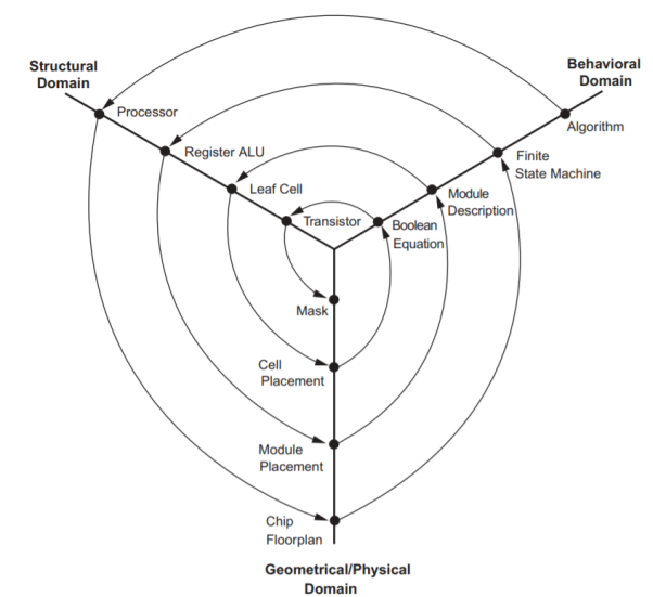
Fig: Y Diagram
The radial lines on the Y-chart represent three distinct design domains: behavioral, structural, and physical. These domains can be used to describe the design of almost any artifact and thus form a very general taxonomy for describing the design process. Within each domain there are a number of levels of design abstraction that start at a very high level and descend eventually to the individual elements that need to be aggregated to yield the top level function (i.e., in the case of chip design and transistors). The behavioral domain describes what a particular system does. For instance, at the highest level we might state that we desire to build a chip that can generate audio tones of specific frequencies (i.e., a touch-tone generator for a telephone). This behavior can be successively refined to more precisely describe what needs to be done in order to build the tone generator (i.e., the frequencies desired, output levels, distortion allowed, etc.). At each abstraction level, a corresponding structural description can be described. The structural domain describes the interconnection of modules necessary to achieve a particular behavior.
For instance, at the highest level, the touch-tone generator might consist of a keyboard, a tone generator, an audio amplifier, a battery, and a speaker. Eventually at lower levels of abstraction, the individual gate and then transistor connections required to build the tone generator are described. For each level of abstraction, the physical domain description explains how to physically construct that level of abstraction. At high levels this might consist of an engineering drawing showing how to put together the keyboard, tone generator chip, battery, and speaker in the associated housing. At the top chip level, this might consist of a floorplan, and at lower levels, the actual geometry of individual transistors. The design process can be viewed as making transformations from one domain to another while maintaining the equivalency of the domains.
Behavioral descriptions are transformed to structural descriptions, which in turn are transformed to physical descriptions. These transformations can be manual or automatic. In either case, it is normal design practice to verify the transformation of one domain to the other by some checking process. This ensures that the design intent is carried across the domain boundaries. Hierarchically specifying each domain at successively detailed levels of abstraction allows us to design very large systems.
The reason for strictly describing the domains and levels of abstraction is to define a precise design process in which the final function of the system can be traced all the way back to the initial behavioral description. There should be no opportunity to produce an incorrect design. If anomalies arise, the design process is corrected so that those anomalies will not reoccur in the future. A designer should acquire a rigid discipline with respect to the design process, and be aware of each transformation and how and why it is failproof.
Normally, these steps are fully automated in a modern design process, but it is important to be aware of the basis for these steps in order to debug them if they go astray. The Y diagram can be used to illustrate each domain and the transformations between domains at varying levels of design abstraction. As the design process winds its way from the outer to inner rings, it proceeds from higher to lower levels of abstraction and hierarchy. Most of the remainder of this chapter is a case study in the design of a simple microprocessor to illustrate the various aspects of VLSI design applied to a nontrivial system. We begin by describing the architecture and microarchitecture of the processor. We then consider logic design and discuss hardware description languages. We continue exploring the physical design of the processor including floor planning and area estimation. Design verification is very important and happens at each level of the hierarchy for each element of the design. Finally, the layout is converted into masks so the chip can be manufactured, packaged, and tested.
Q18) Compare nmos and pmos transistors?
A18)
Region | NMOS | PMOs |
Cut-off |   |    |
Linear |     |      |
Saturation |     |      |
Q19) State Moore’s law and give small description on levels of integration?
A19) Moore’s Law The number of transistors embedded on the chip doubles after every one and a half years. The number of transistors is taken on the y-axis and the years in taken on the x-axis. The diagram also shows the speed in MHz. The graph given in figure also shows the variation of speed of the chip in MHz.
MOS (Metal Oxide Silicon) Transistor History 1925: J. Lilienfeld proposed the basic principle of MOS FET (Field Effect Transistor). 1935: O. Heil proposed a similar structure.
1962: P.K. Weimer (RCA) first placed pMOS and nMOS transistors on the same substrate.
1963: Frank Wanlass (Fairchild) invented invertor, NOR and NAND CMOS gates. This invention starts the era of CMOS low power applications.
1965: The first MOS calculator.
1971: Emergence of nMOS-silicon gate technology.
Note: Early research on MOS technology led to success of bipolar transistor. This in turns leads to a decline of interest in MOS transistor.
1980: The market share of MOSFET exceeds bipolar device.
Levels of Integration:
- Small Scale Integration: (10-100) transistors => Example: Logic gates
- Medium Scale Integration: (100-1000) => Example: counters
- Large Scale Integration: (1000-20000) => Example:8-bit chip
- Very Large Scale Integration: (20000-1000000) => Example:16 & 32 bit up
- Ultra Large Scale Integration: (1000000-10000000) => Example: Special processors, virtual reality machines, smart sensors
Q20) What is n well technology explain in detail?
A20) The well-established n-well CMOS fabrication technology, which requires that both nchannel and p-channel transistors be built on the same chip substrate. To accommodate this, special regions are created with a semiconductor type opposite to the substrate type. The regions thus formed are called wells or tubs. In an n-type substrate, we can create a p-well or alternatively, an n-well is created in a p-type substrate. We present here a simple n-well CMOS fabrication technology, in which the NMOS transistor is created in the p-type substrate, and the PMOS in the n-well, which is built-in into the p-type substrate. Historically, fabrication started with p-well technology but now it has been completely shifted to n-well technology. The main reason for this is that, "n-well sheet resistance can be made lower than p-well sheet resistance" (electrons are more mobile than holes). The simplified process sequence shown in figure below for the fabrication of CMOS integrated circuits on a p-type silicon substrate is as follows:
• N-well regions are created for PMOS transistors, by impurity implantation into the substrate.
• This is followed by the growth of a thick oxide in the regions surround the NMOS and PMOS active regions.
• The thin gate oxide is subsequently grown on the surface through thermal oxidation.
• After this n+ and p+ regions (source, drain and channel-stop implants) are created.
• The metallization step (creation of metal interconnects) forms the final step in this process.
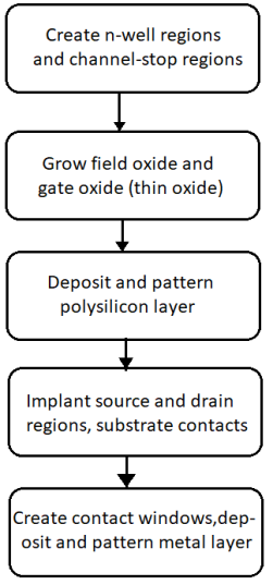
Fig: Simplified Process Sequence for Fabrication of CMOS ICs
The integrated circuit may be viewed as a set of patterned layers of doped silicon, polysilicon, metal and insulating silicon dioxide, since each processing step requires that certain areas are defined on chip by appropriate masks. A layer is patterned before the next layer of material is applied on the chip. A process, called lithography, is used to transfer a pattern to a layer. This must be repeated for every layer, using a different mask, since each layer has its own distinct requirements. We illustrate the fabrication steps involved in patterning silicon dioxide through optical lithography, using Figure below which shows the lithographic sequences.
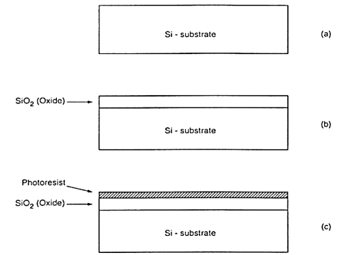
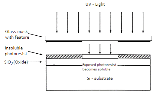
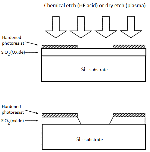

Fig: Process steps required for patterning of silicon dioxide
First an oxide layer is created on the substrate with thermal oxidation of the silicon surface. This oxide surface is then covered with a layer of photoresist. Photoresist is a light-sensitive, acid-resistant organic polymer which is initially insoluble in the developing solution. On exposure to ultraviolet (UV) light, the exposed areas become soluble which can be etched away by etching solvents. Some areas on the surface are covered with a mask during exposure to selectively expose the photoresist. On exposure to UV light, the masked areas are shielded whereas those areas which are not shielded become soluble. There are two types of photoresists, positive and negative photoresist. Positive photoresist is initially insoluble, but becomes soluble after exposure to UV light, whereas negative photoresist is initially soluble but becomes insoluble (hardened) after exposure to UV light. The process sequence described uses positive photoresist.
Negative photoresists are more sensitive to light, but their photolithographic resolution is not as high as that of the positive photoresists. Hence, the use of negative photoresists is less common in manufacturing high-density integrated circuits. The unexposed portions of the photoresist can be removed by a solvent after the UV exposure step. The silicon dioxide regions not covered by the hardened photoresist is etched away by using a chemical solvent (HF acid) or dry etch (plasma etch) process. On completion of this step, we are left with an oxide window which reaches down to the silicon surface. Another solvent is used to strip away the remaining photoresist from the silicon dioxide surface. The patterned silicon dioxide feature is shown in Figure below.
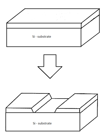
Fig: The result of single photolithographic patterning sequence on silicon dioxide
The sequence of process steps illustrated in detail actually accomplishes a single pattern transfer onto the silicon dioxide surface. The fabrication of semiconductor devices requires several such pattern transfers to be performed on silicon dioxide, polysilicon, and metal. The basic patterning process used in all fabrication steps, however, is quite similar to the one described earlier. Also note that for accurate generation of high density patterns required in submicron devices, electron beam (E-beam) lithography is used instead of optical lithography. In this section, we will examine the main processing steps involved in fabrication of an n-channel MOS transistor on a p-type silicon substrate.
The first step of the process is the oxidation of the silicon substrate (Fig(a) below), which creates a relatively thick silicon dioxide layer on the surface. This oxide layer is called field oxide (Fig(b) below). The field oxide is then selectively etched to expose the silicon surface on which the transistor will be created (Fig.(c) below). After this the surface is covered with a thin, high-quality oxide layer. This oxide layer will form the gate oxide of the MOS transistor (Fig(d) below). Then a polysilicon layer is deposited on the thin oxide (Fig(e) below). Polysilicon is used as both a gate electrode material for MOS transistors as well as an interconnect medium in silicon integrated circuits. The resistivity of polysilicon, which is usually high, is reduced by doping it with impurity atoms. Deposition is followed by patterning and etching of polysilicon layer to form the interconnects and the MOS transistor gates (Fig.(f) below). The thin gate oxide not masked by polysilicon is also etched away exposing the bare silicon surface. The drain and source junctions are to be formed (Fig(g) below). Diffusion or ion implantation is used to dope the entire silicon surface with a high concentration of impurities (in this case donor atoms to produce n-type doping). Fig(h) below shows two n-type regions (source and drain junctions) in the p-type substrate as doping penetrates the exposed areas of the silicon surface. The penetration of impurity doping into the polysilicon reduces its resistivity. The polysilicon gate is patterned before the doping and it precisely defines the location of the channel region and hence, the location of the source and drain regions. Hence this process is called a self-aligning process. The entire surface is again covered with an insulating layer of silicon dioxide after the source and drain regions are completed (Fig (i) below). Next contact windows for the source and drain are patterned into the oxide layer (Fig. (j) below). Interconnects are formed by evaporating aluminium on the surface (Fig(k) below), which is followed by patterning and etching of the metal layer (Fig(l) below). A second or third layer of metallic interconnect can also be added after adding another oxide layer, cutting (via) holes, depositing and patterning the metal.
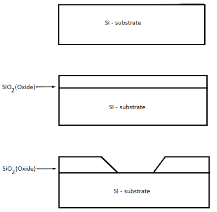
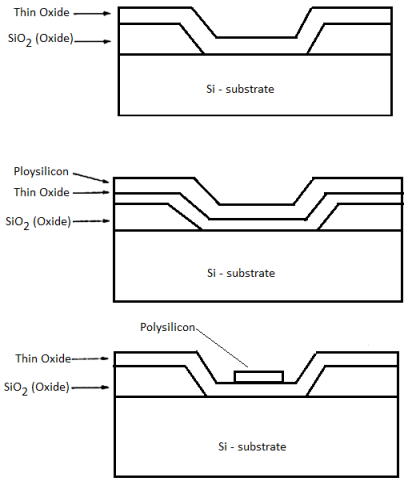
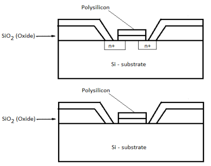
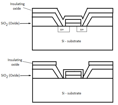
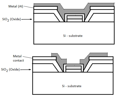
Fig: Process flow for the fabrication of an n-type MOSFET on p-type silicon
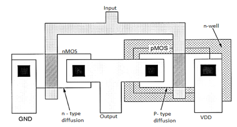
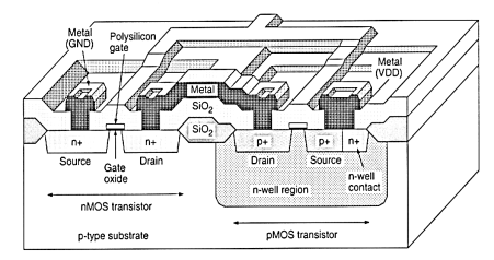
We now return to the generalized fabrication sequence of n-well CMOS integrated circuits. The following figures illustrate some of the important process steps of the fabrication of a CMOS inverter by a top view of the lithographic masks and a cross-sectional view of the relevant areas. The n-well CMOS process starts with a moderately doped (with impurity concentration typically less than 1015 cm-3) p-type silicon substrate. Then, an initial oxide layer is grown on the entire surface. The first lithographic mask defines the n-well region. Donor atoms, usually phosphorus, are implanted through this window in the oxide. Once the n-well is created, the active areas of the nMOS and pMOS transistors can be defined
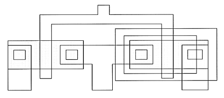
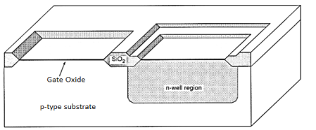
The creation of the n-well region is followed by the growth of a thick field oxide in the areas surrounding the transistor active regions, and a thin gate oxide on top of the active regions. The two most important critical fabrication parameters are the thickness and quality of the gate oxide. These strongly affect the operational characteristics of the MOS transistor, as well as its long-term stability. Chemical vapor deposition (CVD) is used for deposition of polysilicon layer and patterned by dry (plasma) etching. The resulting polysilicon lines function as the gate electrodes of the nMOS and the pMOS transistors and their interconnects. The polysilicon gates also act as self-aligned masks for source and drain implantations. The n+ and p+ regions are implanted into the substrate and into the n-well using a set of two masks. Ohmic contacts to the substrate and to the n-well are also implanted in this process step.
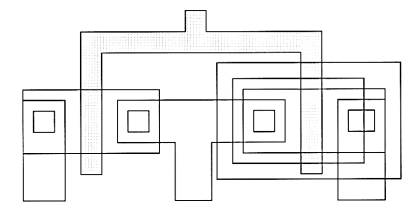
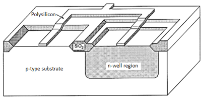
CVD is again used to deposit and insulating silicon dioxide layer over the entire wafer. After this the contacts are defined and etched away exposing the silicon or polysilicon contact windows. These contact windows are essential to complete the circuit interconnections using the metal layer, which is patterned in the next step. Metal (aluminium) is deposited over the entire chip surface using metal evaporation, and the metal lines are patterned through etching. Since the wafer surface is non-planar, the quality and the integrity of the metal lines created in this step are very critical and are ultimately essential for circuit reliability. The composite layout and the resulting cross-sectional view of the chip, showing one nMOS and one pMOS transistor (built-in n-well), the polysilicon and metal interconnections. The final step is to deposit the passivation layer (for protection) over the chip, except for wire-bonding pad areas. This completes the fabrication of the CMOS inverter using n-well technology.
