Unit - 2
Delay
Q1) Consider the CMOS inverter circuit shown in Figure, with VDD = 3.3 V. The I-V characteristics of the nMOS transistor are specified as follows: when VGS = 3.3 V, the drain current reaches its saturation level Isat = 2 mA for VDS 2.5 V. Assume that the input signal applied to the gate is a step pulse that switches instantaneously from 0 V to 3.3 V. Using the data above, calculate the delay time necessary for the output to fall from its initial value of 3.3 V to 1.65 V, assuming an output load capacitance of 300 pF.
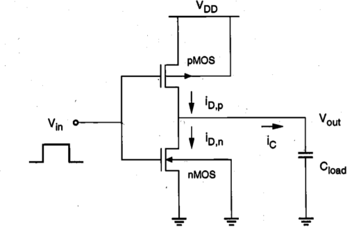
A1) For the solution, consider the simplified pull-down circuit shown above in explanation of the section. We will assume that the nMOS transistor operates in saturation from t = 0 to t = tsat= t1’, and that it will operate in the linear region from t = tsat= t1’ to t = t2 = tdelay. We can also deduce from the I-V characteristics that VT,n = 0.8 V, since the nMOS transistor enters saturation when VDS > VGS - VT,,. The voltage VGS is equal to 3.3 V for t 0
0
The current equation for the saturation region can be written as

We can calculate the amount of time in which the nMOS transistor operates in saturation (tsat), by integrating this equation. The average-current method presented earlier in this Section can also be used to estimate the propagation delay times as well as the rise and fall times of inverter circuits.
Q2) For the CMOS inverter shown in Figure with a power supply voltage of VDD = 5 V, determine the fall time  fall which is defined as the time elapsed between the time point at which Vout = V90% = 4.5 V and the time point at which VOut = Vl0% = 0.5 V. Use both the average-current method and the differential equation method for calculating
  fall. The output load capacitance is 1 pF. The nMOS transistor parameters are given as
  n Cox = 20,uA/V2 (W/L)n = 10, VT,n = 1.0 V

A2) We can determine the average capacitor current during the charge-down event described above.


The fall time is then found as

Now, we will recalculate the fall time using the differential equation approach. The nMOS transistor operates in the saturation region for 4.0 V < Vout < 4.5 V. Writing the current equation for the saturation region, we obtain
 , where

Integrating this simple expression yields the time during which the nMOS transistor operates in saturation.


The nMOS transistor operates in the linear region for  . The current equation for this operating region is written as follows:

Integrating this equation, we obtain the delay component during which the nMOS transistor operates in the linear region.


Thus, the fall time of the CMOS inverter is found as follows:

Q3) A company in Urbana, IL called Prairie Technology has access to a CMOS fabrication process with the device parameters listed below.


 for both nMOS and pMOS devices


Design a CMOS inverter by determining the channel widths W, and Wp of the nMOS and pMOS transistors, to meet the following performance specifications.
 for
for 
- Propagation delay times
 and
and 
- A failing delay of 0.35 ns for an output transition from 2 V to 0.5V, assuming a combined output load capacitance 300fF and ideal step input.
A3) We start our design by satisfying the time delay constraints. First, the minimum (WIL) ratios of the nMOS and pMOS transistors which are dictated by the propagation delay constraints can be found


During the falling output transition (from 2 V to 0.5 V) described above, the nMOS transistor of the CMOS inverter will operate entirely in the linear region. The current equation of the nMOS transistor in this region is

By integrating this expression, we obtain the following relationship


Now we solve this equation for the nMOS transistor (W/L) ratio:

Notice that this ratio is smaller than the (W/L)-ratio found from the propagation delay constraint. Thus, we take the larger ratio which will satify both timing constraints, and determine the size of the nMOS transistor as Wn = 4.7  m, for the given Ln, = 0.6
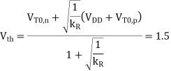
  m. Next, the logic threshold constraint of Vth = 1.5 V will help determine the pMOS transistor dimensions.
Thus, the total capacitive load of the inverter can now be expressed as


The falling and rising output transitions are rewritten as


Note that the channel lengths Ln and LP are usually fixed and equal to each other. Also, the ratio between the channel widths Wn and Wp is usualy dictated by other design constraints such as noise margins and the logic inversion threshold. Let this transistor aspect ratio be defined as


The propagation delay times of a CMOS inverter cannot be reduced'beyond these limit values, which are dictated by technology-related parameters such as doping densities, minimum channel length and minimum layout design rules (e.g., Ddrain). Also, note that the propagation delay limit is independent of the extrinsic capacitance components, Ci,. And Cg. How fast this asymptotic limit is approached in a specific case depends on the ratio of intrinsic and extrinsic capacitance components of Cload. If the extrinsic components dominate the total load capacitance, then delay reduction can be achieved for wider range of Wn and We. If, on the other hand, the intrinsic capacitance component is dominant, then the speed limit is reached for smaller values of Wn and Wp
Q4) Calculate the output voltage rise and fall times for CMOS inverter?
A4) The input and output voltage waveforms of a typical inverter circuit are shown in Figure below. The propagation delay times  PHL and
  PLH determine the input-to-output signal delay during the high-to-low and low-to-high transitions of the output, respectively. By definition,
  PHL is the time delay between the V50%-transition of the rising input voltage and the V50% -transition of the falling output voltage. Similarly,
  PLH is defined as the time delay between the V50% -transition of the falling input voltage and the V50%-transition of the rising output voltage. To simplify the analysis and the derivation of delay expressions, the input voltage waveform is usually assumed to be an ideal step pulse with zero rise and fall times. Under this assumption, TPHL becomes the time required for the output voltage to fall from VOH to the V50% level, and
  PLH becomes the time required for the output voltage to rise from VOL to the V50% level. The voltage point V50% is defined as follows.
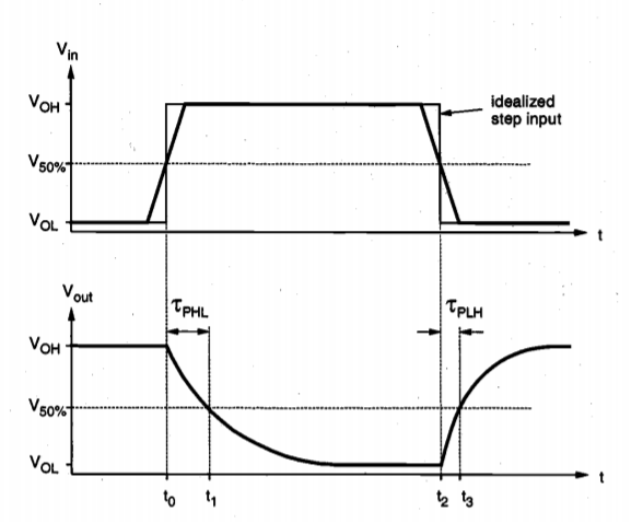
Fig: Input and output voltage waveforms of a typical inverter, and the definitions of propagation delay times. The input voltage waveform is idealized as a step pulse for simplicity.

Thus, the propagation delay times  PHL and
  PLH are found from Figure above as


The average propagation delay of  p the inverter characterizes the average time required for the input signal to propagate through the inverter.

We will refer to Figure below for the definition of output voltage rise and fall times. The rise I time  rise is defined here as the time required for the output voltage to rise from the V10% level to V90% level. Similarly, the fall time Tall is defined here as the time required for the output voltage to drop from the V90% level to V10% level. The voltage levels V10% and V90% are defined as


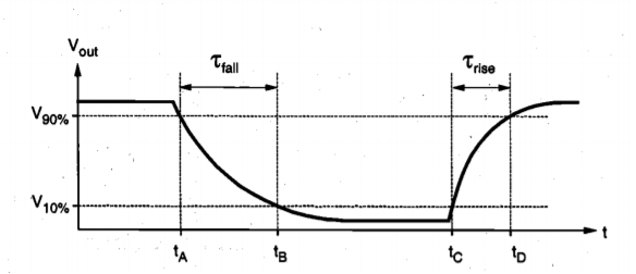
Fig: Output voltage rise and fall times.
Thus, the output rise and fall times are found from Figure above as follows.


Q5) Derive the expression for propagation delay calculated for CMOS inverter?
A5) The simplest approach for calculating the propagation delay times  pHL and
  pLH is based on estimating the average capacitance current during charge down and charge up, respectively. If the capacitance current during an output transition is approximated by a constant average current Iavg the delay times are found as


The average current during high-to-low transition can be calculated by using the current values at the beginning and the end of the transition.

Similarly, the average capacitance current during low-to-high transition is

The propagation delay times can be found more accurately by solving the state equation of the output node in the time domain. The differential equation associated with the output node is given below. Note that the capacitance current is also a function of the output voltage.

First, we consider the rising-input case for a CMOS inverter. Initially, the output Voltage is assumed to be equal to VOH. When the input voltage switches from low (VOL) to high (VOH), the nMOS transistor is turned on and it starts to discharge the load 0 capacitance. At the same time, the pMOS transistor is switched off; thus,


Note that in other types of inverter circuits, such as the resistive-load inverter or the depletion-load inverter, the load device continues to conduct a nonzero current when the input is switched from low to high. However, the load current is usually negligible in comparison to the driver current. Therefore, above equation can be used to calculate the charge- down time not only in CMOS inverters, but also in almost all common types of inverter circuits.
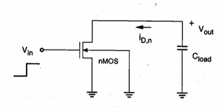
Fig: Equivalent circuit of the CMOS inverter during high-to-low output transition.
First, consider the nMOS transistor operating in saturation

For 
Since the saturation current is practically independent of the output voltage (neglecting channel-length modulation),


Evaluating this simple integral yields

At t = t', the output voltage will be equal to (VDD - VTn) and the transistor will be at the saturation-linear region boundary. Next, consider the nMOS transistor operating in the linear region.


The solution in the time interval between t' and t can be found as


Evaluating this integral yields


The transconductance kn of the nMOS transistor can be found as follows:

Now, the current equation for the linear operating region is

Integrating this differential equation between the two voltage boundary conditions yields the time in which the nMOS transistor operates in the linear region during this transition.


Thus, the total delay time is found to be

Note that tdelay corresponds to the propagation delay time  PHL for falling output.

Finally, the propagation delay time for high-to-low output transition ( PHL) can be found by

For VOH = VDD and VOL= 0, as is the case for the CMOS inverter

Q6) What is RC delay model explain?
A6)
- The RC delay model is a metric used in VLSI design to calculate the signal delay between the input voltage and output voltage of the input signal.
- The input signal is a step function. In this case the transistor can be considered as a switch in series with a resistor.
- A unit nMOS transistor is characterized with resistance or effective resistance, R= Vds/Ids
- Let’s consider a k times transistor unit, here the resistor of the single transistor is R/k, k is the constant here. PMOS transistor has a bigger resistance – 2R.
- NMOS transistors are characterized with higher mobility than pMOS transistors. If the transistor is velocity-saturated, its current and resistance does not depend on the channel length.
- Let’s consider a transistor with gate capacitance C. For a k unit cell, gate capacitance of the transistor is kC.
- Diffusion capacitance depends on the size of drain or source, but with the most common approximation it is also C.
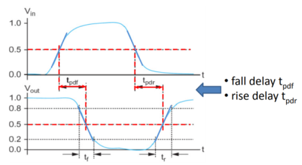
Fig: Time Delay
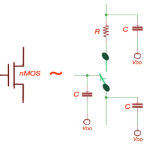
Fig: RC Circuit
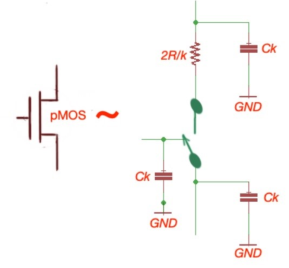
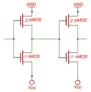
Fig: Equivalent RC circuits
Q7) Explain Static power consumption of a CMOS inverter?
A7) Static Power Consumption
Typically, all low-voltage devices have a CMOS inverter in the input and output stage. Therefore, for a clear understanding of static power consumption, refer to the CMOS inverter modes shown in Figure.
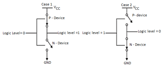
Fig: CMOS inverter mode for Static Power Consumption
As shown in Figure above, if the input is at logic 0, the n-MOS device is OFF, and the p-MOS device is ON (Case 1). The output voltage is VCC, or logic 1. Similarly, when the input is at logic 1, the associated n-MOS device is biased ON and the p-MOS device is OFF. The output voltage is GND, or logic 0. Note that one of the transistors is always OFF when the gate is in either of these logic states. Since no current flows into the gate terminal, and there is no dc current path from VCC to GND, the resultant quiescent (steady-state) current is zero, hence, static power consumption (Pq) is zero.
However, there is a small amount of static power consumption due to reverse-bias leakage between diffused regions and the substrate. This leakage inside a device can be explained with a simple model that describes the parasitic diodes of a CMOS inverter, as shown in Figure below.
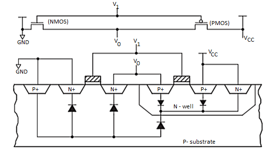
Fig: Model Describing Parasitic Diodes Present in CMOS Inverter
The source drain diffusion and N-well diffusion form parasitic diodes. In Figure above, the parasitic diodes are shown between the N-well and substrate. Because parasitic diodes are reverse biased, only their leakage currents contribute to static power consumption. The leakage current (llkg)of the diode is described by the following equation:

Where
 reverse saturation current
V = diode voltage
k= Boltzmann’s constant (1.38×
q= electronic charge (1.602 ×  )
)
T = temperature
Static power consumption is the product of the device leakage current and the supply voltage. Total static power consumption, PS, can be obtained as shown in equation
Ps = 
Most CMOS data sheets specify an ICC maximum in the 10-µA to 40-µA range, encompassing total leakage current and other circuit features that may require some static current not considered in the simple inverter model.
The leakage current ICC (current into a device), along with the supply voltage, causes static power consumption in the CMOS devices. This static power consumption is defined as quiescent, or PS, and can be calculated by equation
Ps = Vcc x Icc
VCC = supply voltage
ICC = current into a device
Q8) Explain dynamic power consumption of CMOS inverter?
A8) The dynamic power consumption of a CMOS IC is calculated by adding the transient power consumption (PT), and capacitive-load power consumption (PL).
Transient Power Consumption
Transient power consumption is due to the current that flows only when the transistors of the devices are switching from one logic state to another. This is a result of the current required to charge the internal nodes (switching current) plus the through current (current that flows from VCC to GND when the p-channel transistor and n-channel transistor turn on briefly at the same time during the logic transition).
The frequency at which the device is switching, plus the rise and fall times of the input signal, as well as the internal nodes of the device, have a direct effect on the duration of the current spike. For fast input transition rates, the through current of the gate is negligible compared to the switching current. For this reason, the dynamic supply current is governed by the internal capacitance of the IC and the charge and discharge current of the load capacitance. Transient power consumption can be calculated using equation
PT = Cpd x VCC2 x f1 x NSW
Where:
PT = transient power consumption
VCC = supply voltage
fI = input signal frequency
NSW = number of bits switching
Cpd = dynamic power-dissipation capacitance
Capacitive-Load Power Consumption
Additional power is consumed in charging external load capacitance and is dependent on switching frequency. The following equation can be used to calculate this power if all outputs have the same load and are switching at the same output frequency.
PL = CL x VCC2 x fo x NSW (CL is the load per output)
Where:
PL = capacitive-load power consumption
VCC = supply voltage
fO = output signal frequency
CL = external (load) capacitance
NSW = total number of outputs switching
In the case of different loads and different output frequencies at all outputs, above equation is used to calculate capacitive-load power consumption.

Where
 = sum of n different frequencies and loads at n different outputs
 all different output frequencies at each output, numbered 1 through n (Hz)
 supply voltage (V)
 all different load capacitances at each output, numbered 1 through n.
Therefore, dynamic power consumption (PD) is the sum of these two power consumptions and can be expressed as shown


 power- consumption capacitance (F)
 input frequency (Hz)
 all different output frequencies at each output, numbered 1 through n (Hz)
 total number of outputs switching
 supply voltage (V)
 all different load capacitances at each output, numbered 1 through n
Total power consumption is the sum of static and dynamic power consumption.

Q9) Explain current signal flow analysis?
A9) Current signal flow analysis
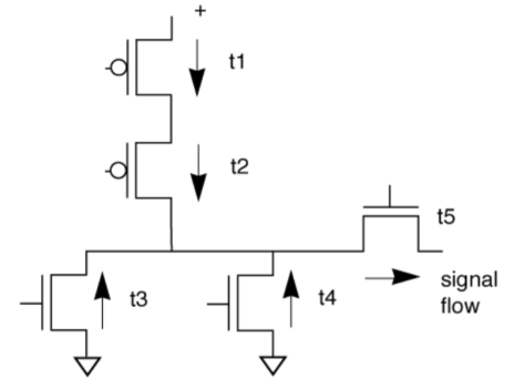
False current path example
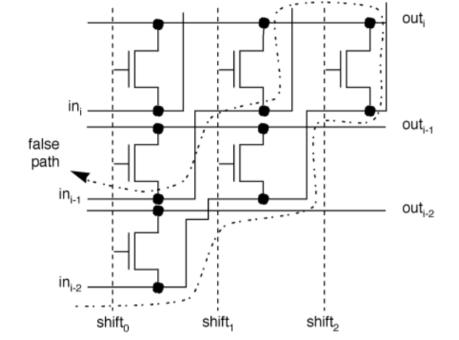
- Many paths in barrel shifter cannot be exercised.
- Driver gates enforce current flow in one direction on data lines, eliminating some paths through the pass transistors.
- Path analysis which does not take into account feasible current flow will identify infeasible long paths.
Q10) Explain the timing analysis procedure?
A10) Timing analysis procedure
Two major steps:
- Build graph with elemental delays;
- Traverse graph to find longest path.
Must model 0-1 and 1-0 delays independently for more accurate total delay. Use value analysis to prune impossible paths.
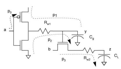
From above example
- Make assumptions about primary inputs.
- Primitive path delay: RC delay from power supply or primary input to transistor gate or primary output. Primitive path (p0, p1, p2, p3) delays computed from RC analysis.
- Each path forms an edge in timing analysis graph.
- Timing analysis graph is analyzed to find worst-case delay through entire circuit.
- Timing graph structure: The nodes are sources and sinks of primitive delay paths. The edges represent primitive delay paths.
- Use depth-first or breadth-first search to find longest delay path.
- False paths create un exercisable paths which make delay pessimistic. Can be identified using analysis algorithms.
- Some transistor configurations only allow current flow in one direction other direction of current/signal flow is a false path.
Q11) What is timing optimisation?
A11) Timing optimisation
The design structures must always contain the paths that are fast enough or the ones that are critical in terms of the operating times – they are called critical paths. The critical paths can be affected at the following levels:
- Architectural level
- Logic level
- Circuit level
- Layout level.
The best leverage is performed with the good microarchitecture. This level requires the broad knowledge of the both the algorithmic and technological level of the device. The next level is logic. The trade-offs can be made at the stage of the functional blocks, the number of stages of gates in the clock cycle, and at the fan-in and fan-out cycles. The delay can be also be turned at the circuit level, varying the transistor size or using different CMOS techniques. The last level is layout level, when the delay can be set up. Here the delay can be set up with the wiring lengths.
Many device designers never leave the RTL level that creates the design. The standard way to write RTL code is to synthesise it and check if the results are fast enough. The timing analysers are used to check the timing closure, and whether the circuit meets the timing requirements. The lower abstraction level is the best way to adjust and vary the timing parameters.
Q12) Explain the cascaded CMOS inverter stages?
A12) Consider the cascade connection of two CMOS inverter circuits shown in Figure below. The parasitic capacitances associated with each MOSFET are illustrated individually. Here the capacitances Cgd and Cgs are primarily due to gate overlap with diffusion, while Cdb and Csb are voltage-dependent junction capacitances. The 'capacitance component Cg is due to the thin-oxide capacitance over the gate area. In addition, we also consider the lumped interconnect capacitance Cint, which represents the parasitic capacitance contribution of the metal or polysilicon connection between the two inverters. It is assumed that a pulse waveform is applied to the input of the first-stage inverter. We wish to analyze the time-domain behavior of the first-stage output, Vout.
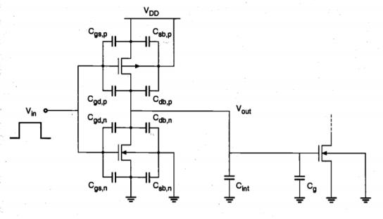
Fig: Cascaded CMOS inverter stages.
The problem of analyzing the output voltage waveform is fairly complicated, even for this relatively simple circuit, because a number of nonlinear, voltage-dependent capacitances are involved. To simplify the problem, we first combine the capacitances seen in Figure above into an equivalent lumped linear capacitance, connected between the output node of the inverter and the ground. This combined capacitance at the output node will be called the load capacitance, Cload.

Note that some of the parasitic capacitance components shown in Figure above do not appear in this lumped capacitance expression. In particular, Csbn and CSb have no effect on the transient behavior of the circuit since the source-to-substrate voltages of both transistors are always equal to zero.
The first-stage CMOS inverter is shown with the single lumped output load capacitance Cload in Figure below. Now, the problem of analyzing the switching behavior can be handled more easily. In fact, the question of inverter transient response is reduced to finding the charge-up and charge-down times of a single capacitance which is charged and discharged through one transistor. The delay times calculated using Cload may slightly overestimate the actual inverter delay, but this is not considered a significant deficiency in a first-order approximation.
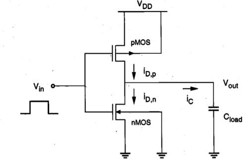
Fig: First-stage CMOS inverter with lumped output load capacitance.
Q13) Draw the DC transfer characteristics of CMOS inverter
A13)
The VTC is divided into five regions (1-5) for easy of understanding. The above shown curve is possible when both T1 and T2 are matched for optimum operation. Optimum operation is achieved when Vin = Vdd/2 we get Vout = Vdd/2. This can be achieved by adjusting width and length of both T1 and T2 as other parameters like mobility, oxide capacitance varies between different technologies.
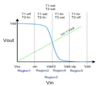
Fig: DC Transfer Characteristics
Region-1
In this, the input is in the range of (0, Vtn).
- NMOS is in cutoff as Vgs < Vtn
- PMOS is in linear as Vgsp < Vtp and Vdsp > Vgsp -Vtp.
- Zero current flows from supply voltage and the power dissipation is zero.
Region-2
Here, the input is in the range of (Vtn,Vdd/2).
- NMOS is in saturation as Vgs > Vtn and Vout >Vin – Vtn.
- PMOS is in linear region as Vdsp > Vgsp -Vtp.
- Since both the transistors are conducting some amount of current flows from supply in this region.
Region-3
Here the input voltage is Vdd/2. At this point the output voltage is Vdd/2. Here both the NMOS and PMOS are in saturation and the output drops drastically from Vdd to Vdd/2. At this point a large amount of current flows from the supply.
- NMOS is in saturation as Vgs > Vtn and Vout >Vin - Vtn.
- PMOS is in saturation as Vgsp < Vtp and Vdsp < Vgsp -Vtp.
- Large amount of current is drawn from supply and hence large power dissipation.
Region-4
In this region the input voltage is in the range of (Vdd/2 , Vdd-Vtp). Here the PMOS remains in saturation as Vout < Vin - Vtp and Vgsp < Vtp. But the NMOS moves from saturation to linear region since the drain to source voltage now is less than Vgsn-Vtn.
- NMOS is in linear as Vgs > Vtn and Vout < Vin - Vtn.
- PMOS is in saturation as Vgsp < Vtp and Vdsp < Vgsp -Vtp.
- A medium amount of current is drawn as NMOS is in linear region and power dissipation is low.
Region-5
In this region the input voltage is in the range of (Vdd-Vtp,Vdd). Here the PMOS moves from saturation to cutoff as the Vgsp is so high that Vgsp > Vtp. The NMOS still remains in linear as the drain to source voltage now is less than Vgsn-Vtn.
- NMOS is in linear as Vgs > Vtn and Vout < Vin - Vtn.
- PMOS is in cutoff as Vgsp > Vtp.
- Zero current flows from the supply and hence the power dissipation is zero.
Q14) Describe the equation for source to drain current in the three regions of operation of a MOS transistor and draw the VI characteristics
A14) We have two types of FETs. They are Enhancement mode and depletion mode transistor. Also, we have PMOS and NMOS transistors.
(i) In Enhancement mode transistor channel is going to form after giving a proper positive gate voltage. We have NMOS and PMOS enhancement transistors.
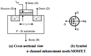
Fig: n-channel enhancement type MOSFET
(ii) In Depletion mode transistor channel will be present by the implant. It can be removed by giving a proper negative gate voltage. We have NMOS and PMOS depletion mode transistors
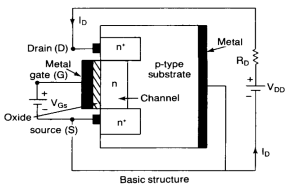
Fig: p-channel depletion MOSFET
Three regions of operation of a MOS transistor
a) Vgs > Vt Vds = 0 Since Vgs > Vt and Vds = 0 the channel is formed but no current flows between drain and source.
b) Vgs > Vt Vds < Vgs - Vt This region is called the non-saturation Region or linear region where the drain current increases linearly with Vds. When Vds is increased the drain, side becomes more reverse biased and the channel starts to pinch. This is called as the pinch off point.
c) Vgs > Vt Vds > Vgs - Vt This region is called Saturation Region where the drain current remains almost constant. Even if the Vds is increased more and more, the increased voltage gets dropped in the depletion region leading to a constant current. The typical threshold voltage for an enhancement mode transistor is given by Vt = 0.2 * Vdd.

Curve
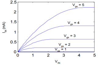
Fig: Vds v/s Ids
Q15) What is Elmore delay?
A15) The Elmore delay analysis model estimates the delay from a source (root) to one of the leaf nodes as the sum of the resistance in the path to the ith node multiplied by the capacitance present at the end of the branch.
Most circuits can be represented as an RC circuit with no loops. As we already stated, the Elmore delay estimates the delay from a source (root) to one of the leaf nodes as the sum of the resistance in the path to the ith node multiplied by the capacitance present at the end of the branch. In other words, the propagation delay from a switching source (root) to an ith branch node is given as the product of the capacitance “Ci” of the node with the sum of the resistance from the source to the node, Ris.
Tpd =
Ris = sum of resistance from source to node i
The 2nd order RC equivalent circuit we considered in the RC delay model:
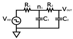
Fig. RC Equivalent
The Elmore delay for Vout is given as tpd = R1C1+(R1+ R2) C2, which is similar to the delay expression gotten for the two-time constant (TTC) approximation model we discussed in the last article.
Let's consider a driver—i.e., a gate that charges or discharges a node or, in other words, a gate that is connected to the input of another gate. For our example, we'll look at a driver which is w-times the unit size which is driving an m-identical inverter. The equivalent RC circuit is shown in Figure below
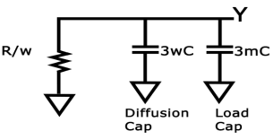
Fig. Equivalent Model

From above equation if we denote the fan-out of the drive to be the ratio between the load capacitance (3mc) and the input capacitance (3wc), we get the following:
h=3mc/3wc=m/w
Tpd = (1+h)3RC
Where τ=3RC.
Q16) What is delay in logic gates explain through waveform?
A16) The propagation delay of a logic gate e.g., inverter is the difference in time (calculated at 50% of input-output transition), when output switches, after application of input.
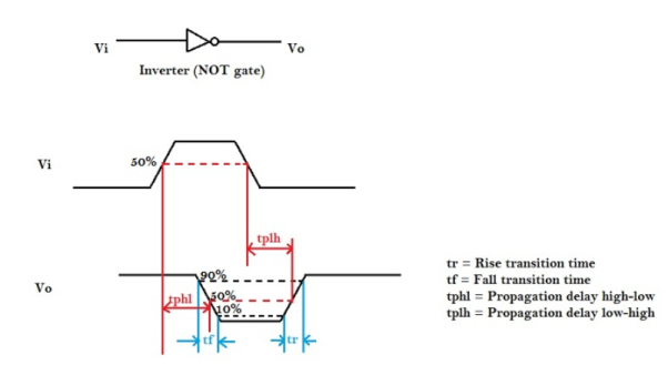
Fig: Propagation Delay
In the above figure, there are 4 timing parameters. Rise time (tr) is the time, during transition, when output switches from 10% to 90% of the maximum value. Fall time (tf) is the time, during transition, when output switches from 90% to 10% of the maximum value. Many designs could also prefer 30% to 70% for rise time and 70% to 30% for fall time. It could vary upto different designs.
The propagation delay high to low (tpHL) is the delay when output switches from high-to-low, after input switches from low-to-high. The delay is usually calculated at 50% point of input-output switching, as shown in above figure.
Now, in order to find the propagation delay, we need a model that matches the delay of inverter. As we have seen above, the switching behavior of CMOS inverter could be modeled as a resistance Ron with a capacitor CL, a simple first order analysis of RC network will help us to model the propagation delay.