Unit - 3
Energy – Delay Optimization
Q1) Compute the sheet resistance of a 0.22 m thick Cu wire in a 65 mm process. Find the total resistance if the wire is 0.125m wide and 1 mm long. Ignore the barrier layer and dishing.
A1)
The sheet resistance is

The total resistance is

Q2) Determine the skin depth for a copper wire in a chip with 20 ps edge rates.
A2) The maximum frequency of interest is


The skin depth will then be calculated as

Q3)10x unit-sized inverter drives a 2x inverter at the end of the 1mm. Suppose that wire capacitance is 0.2 fF/m and that unit-sized nMOS transistor has R10k and C=0.1Ff. Estimate the propagation delay using the Elmore delay model; neglect diffusion capacitance.
A3)
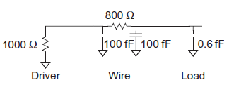
The driver has a resistance of 1k. The receiver has a 2-Unit nMOS transistor and a 4-unit pMOS transistor, for a capacitance of 0.6Ff. The wire capacitance is 200Ff.
Figure shows an equivalent circuit for the system using a single-segment π-model. The Elmore delay is  The capacitance of the long wire dominates the delay; the capacitance of the 2x inverter is negligible in comparison.
Because both wire resistance and wire capacitance increase with length, wire delay grows quadratically with length. Using thicker and wider wires, lower-resistance metals such as copper, and lower-dielectric constant insulators helps, but long wires nevertheless often have unacceptable delay.
Q4) Find RC flight time per  for a wire using the parameters form example above express the result in FO4
 , if the FO4 inverter delay is 15ps. What is the flight time to cross a 10mm die?
A4)
R=800/mm, C=0.2 pF/mm. The flight time is RC/2=80ps/ ,or 5.3 FO
 . The flight time across a 10mm die is thus 530 FO4, which is dozens of clock cycles.
Q5) Figure models a gate driving wires to destinations. The gate is represented as a voltage source with effective resistance  . The two receivers are located at nodes 3 and 4. The wire to node 3 is long enough that it is represented with a pair of π-segments, while the wire to node 4 is representation with a single segment. Find the Elmore delay from input x to each receiver.
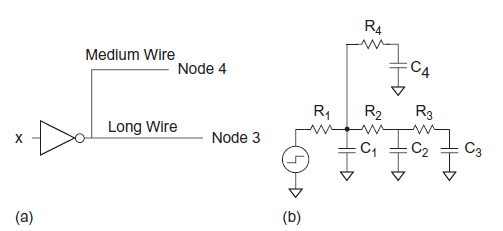
A5)
The elmore delays are


Q6) Estimate the energy per unit length to send a bit of information (one rising and one falling transition) in a CMOS process.
A6)
E = (0.2 pF/mm) (1.0 V)2 = 0.2 pJ/bit/mm.
Sometimes energy in a communication link is expressed as power per gigabit per second: 0.2 mW/Gbps.
Q7) Consider a microprocessor on a 20 mm × 20 mm die running at 3 GHz in the 65 nm process. A layer of metal is routed on a 250 nm pitch. Half of the available wire tracks are used. The wires have an average activity factor of 0.1. Determine the power consumed by the layer of metal.
A7) There are (20 mm) / (250 nm) = 80,000 tracks of metal across the die, of which 40,000 are occupied. The wire capacitance is (0.2 pF/mm)(20 mm)(40,000 tracks) = 160 nF. The power is (0.1)(160 nF)(1.0 V)2(3 GHz) = 48 W. This is clearly a problem, especially considering that the chip has more than one layer of metal. The activity factor needs to be much lower to keep power under control.
Q8) Each wire in a pair of 1 mm lines has capacitance of 0.08 fF/ m to ground and 0.12 fF/
 m to its neighbor. Each line is driven by an inverter with a 1 k
 effective resistance. Estimate the contamination and propagation delays of the path. Neglect parasitic capacitance of the inverter and resistance of the wires.
A8) We find Cgnd = (0.08 fF/ m) (1000
  m) = 80 fF and Cadj = 120 fF. The delay is RCeff. The contamination delay is the minimum possible delay, which occurs when both wires switch in the same direction.
In that case, Ceff = Cgnd and the delay is tcd = (1 k )(0.08 pF) = 80 ps. The propagation delay is the maximum possible delay, which occurs when both wires switch in opposite directions.
In this case, Ceff = Cgnd + 2Cadj and the delay is tpd = (1 k )(0.32 pF) = 320 ps. This is a factor of four difference between best and worst case.
Q9) Compute the delay per mm of a repeated wire in a 65 nm process. Assume the wire is on a middle routing layer and has 2x width, spacing, and height, so its resistance is 200  /mm and capacitance is 0.2 pF/mm. The FO4 inverter delay is 15 ps. Also find the repeater spacing and driver size to achieve this delay and the energy per bit.
A9) The delay is

This delay is achieved using a spacing of 0.45 mm between repeaters and an nMOS
Driver width of 18  m (180x unit size). The energy per bit is 0.4 pJ/mm.
Q10) The path in Figure contains a medium-length wire modeled as a lumped capacitance. Write an equation for path delay in terms of x and y. How large should the x and y inverters be for shortest path delay? What is the stage effort of each stage?

Fig: Path with medium-length wire
A10)
From the Logical Effort delay model, we find the path delay is

Differentiating with respect to each size and setting the results to 0 allows us to solve equation for x = 33 fF and y = 57 Ff.


The stage efforts are (33/10) = 3.3, (57 +50)/33 = 3.2, and (100/57) = 1.8. Notice that the first two stage efforts are equal as usual, but the third stage effort is lower. As x already drives a large wire capacitance, y may be rather large and will bear a small stage effort) before the incremental increase in delay of x driving y equals the incremental decreases in delay of y driving the output.
Q11) What is minimum energy delay product and how it is helpful for energy-delay optimisation?
A11) Minimum Energy Delay Product
The energy-delay product (EDP) is a popular metric that balances the importance of energy and delay. Neglecting leakage, we can elegantly solve for the supply voltage that minimizes EDP. Considering leakage, the best supply voltage is slightly higher. First, consider the EDP when leakage is negligible. The energy to charge a load capacitance Ceff is given. The delay, using an α-power law model, is given. Thus, the EDP is

Differentiating with respect to VDD and setting the result to 0 gives the voltage at which
The EDP is minimized

The above equation suggests that the EDP improves as Vt approaches 0, which is obviously not true because leakage power would dominate. When a leakage term is incorporated into above equation, the results become too messy to reprint here.
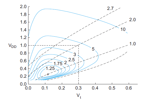
Fig 1 Contours of energy-delay product
Figure shows contours of EDP and delay as a function of VDD and Vt. EDP is normalized to the best achievable. For typical process parameters, the best Vt is about 100–150 mV and the EDP is about four times better than at a typical operating point of VDD = 1.0 V and Vt = 0.3 V. At the optimum, leakage energy is about half of dynamic energy. The dashed lines indicate contours of equal speed, normalized to the speed at the best EDP point. To operate at higher speed requires increasing the EDP.
Minimum Energy Under Delay Constraints
In practice, designers generally face the problem of achieving minimum energy under a delay constraint. Equivalently, the power consumption of the system is limited by battery or cooling considerations and the designer seeks to achieve minimum delay under an energy constraint. Figure 2(a) showed contours of delay and energy. The best supply voltage and threshold for operation at a given delay is where the delay and energy contours are tangent. For a given supply voltage and threshold voltage, the designer can make logic and sizing choices that affect delay and energy. Such curves can be generated using a logic synthesizer or sizing tool constrained to various delays. The curve becomes steep near the point of minimum delay, so energy-efficient designs should aim to operate at a longer delay. Energy under a delay constraint is also minimized when leakage is about half of dynamic power. However, the curve is fairly flat around this point, so many designs operate at lower leakage to facilitate power saving during sleep mode.
Q12) Derive the equation for minimum energy required and minimum operating voltage required under delay constraints?
A12) The product of the power of an operation and the time for the operation to complete is the energy consumed. Hence, the power-delay product (PDP) is simply the energy. The minimum energy point is the least energy that an operation could consume if delay were unimportant. It occurs in subthreshold operation where VDD < Vt. The minimum energy point typically consumes an order of magnitude less energy than the conventional operating point, but runs at least three orders of magnitude more slowly.
John von Neumann first asserted (without justification) that the “thermodynamic
Minimum of energy per elementary act of information” was kT ln2. Meindl proved this result for CMOS by considering the minimum allowable voltage at which an inverter could operate. To achieve nonzero noise margins, an inverter must have a slope steeper than –1 at the switching point, Vinv . For an ideal inverter with n = 1 in the subthreshold characteristics, this occurs at a minimum operating voltage of
Vmin = 2ln 2vT = 36 mV @ 300 K
The energy stored on the gate capacitance of a single MOSFET is E = QVDD/2, where Q is the charge. The minimum possible charge is one electron, q. Substituting Vmin for VDD gives Emin = kT ln 2 = 2.9 × 10⁻²¹ J. In contrast, a unit inverter in a 0.5  m 5 V process draws about 1.5 × 10⁻¹³ J from the supply when switching, and the same inverter in a 65 nm 1 V process draws 3 × 10–16 J.
Inverters have been demonstrated operating with power supplies under 100 mV, but these do not actually minimize energy in a real CMOS process. Although they have extremely low switching energy, they run so slowly that the leakage energy dominates. The true minimum energy point is at a higher voltage that balances switching and leakage energy. In subthreshold operation, the current drops exponentially as VDD – Vt decreases and Thus, the delay increases exponentially. The switching energy improves quadratically with VDD. Leakage current improves slowly with VDD because of DIBL, but the leakage energy increases exponentially because the slower gate leaks for a longer time. To achieve minimum energy operation, all transistors should be minimum width. This reduces both switching capacitance and leakage. Gate and junction leakage and short-circuit power are negligible in subthreshold operation, so the total energy is the sum of the switching and leakage energy, which is minimized near the point they crossover, as shown in Figure
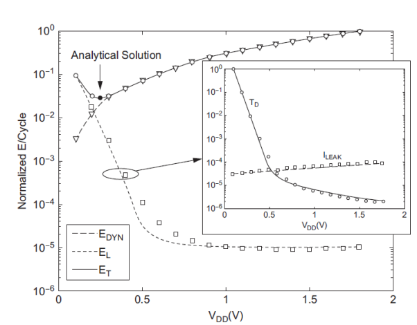
Fig 2 Minimum energy point
To compute the energy, assume that a circuit has N gates on the critical path, a total effective capacitance Ceff, and a total effective width Weff of leaking transistor. The delay of a gate operating subthreshold with a load Cg is given. The cycle time is thus

The energy consumed in one cycle is 


A more intuitive approach is to look at the minimum energy point graphically. Figure (a) plots the energy and delay contours as a function of VDD and Vt for a ring oscillator in a 180 nm process designed to reflect the behavior of a microprocessor pipeline. As VDD increases or Vt decreases, the operating frequency increases exponentially assuming the circuit is operating at or near threshold. At VDD = Vt, the circuit operates at about 10 MHz. The energy contours are normalized to the minimum energy point. This point, marked with a cross, occurs at VDD = 0.13 V and Vt = 0.37 V. The energy is about 10 times lower than at a typical operating point, but the delay is three to four orders of magnitude greater.
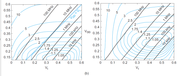
Fig 3 Contours of energy and delay rings
The shape of the curve is only a weak function of process parameters, so it remains valid for nanometer processes. However, the result does depend strongly on the relative switching and leakage energies. Figure (b) plots the results when the activity factor drops to 0.1, reducing Ceff. Switching energy is less important, so the circuit can run at a higher supply voltage. The threshold then increases to cut leakage. The total energy is greatly reduced. The result also depends on temperature: at high temperature, circuits leak more so a higher threshold voltage should be used. Process variation also pushes the best operating point toward higher voltage and energy.
Q13) Explain how parallelism and piping have reduced the power consumption in VLSI?
A13) Parallelism and Piping
In the past, parallelism and pipelining have been effective ways to reduce power consumption, as shown in Figure. Replacing a single functional unit with N parallel units allows each to operate at 1/N the frequency. A multiplexer selects between the results. The voltage can be scaled down accordingly, offering quadratic savings in energy at the expense of doubling the area. Replacing a single functional unit with an N-stage pipelined unit also reduces the amount of logic in a clock cycle at the expense of more registers. Again, the voltage can be scaled down. The two techniques can be combined for even better energy efficiency.
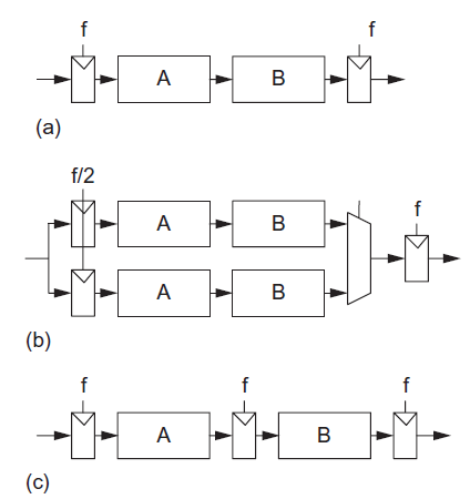
Fig 4 Functional units: (a) normal, (b) parallel, (c) pipelined
When leakage is unimportant, parallelism offers a slight edge because the multiplexer has less overhead than the pipeline registers. Also, perfectly balancing logic across pipeline stages can be difficult. Now that leakage is a substantial fraction of total power, pipelining becomes preferable because the parallel hardware has N times as much leakage. Now that VDD is closer to the best energy-delay point, the potential supply reduction and energy savings are diminishing. Nevertheless, parallelism and pipelining remain primary tools to extract performance from the vast transistor budgets now available.
Q14) How power management is done in chips for efficient power management?
A14) Power Management Modes
Chip designers have now learned they must turn off portions of the chip when they are not active by applying clock and power gating. Many chips now employ a variety of power management modes giving a trade-off between power savings and wake-up time. For example, the Intel Atom processor operates at a peak frequency of 2 GHz at 1 V, consuming 2 W. The power management modes are shown in Figure.
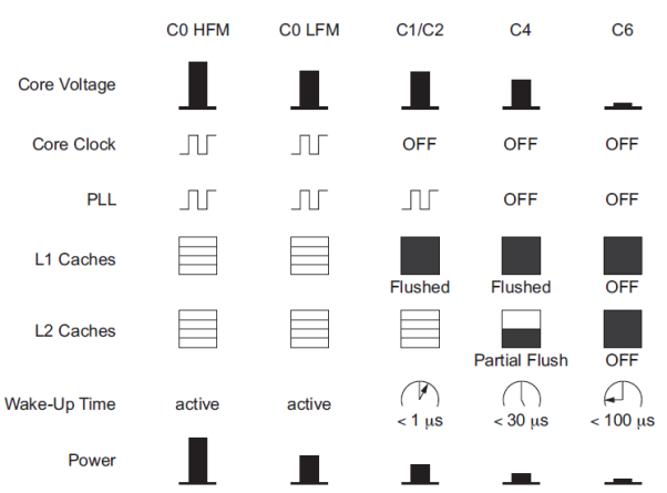
Fig 5 Atom power management modes
In the low frequency mode, the clock drops as slow as 600 MHz while the power supply. Reduces to 0.75 V. In sleep mode C1, the core clock is turned off and the level 1 cache is flushed and power-gated to reduce leakage, but the processor can return to active state in 1 microsecond. In sleep mode C4, the PLL is also turned OFF. In sleep mode C6, the core and caches are all power-gated to reduce power to less than 80 mW, but wake-up time rises to 100 microseconds. For a typical workload, the processor can spend 80–90% of its time in C6 sleep mode, reducing average power to 220 mW.
The worst-case power that a chip may consume can be a factor of two or more greater than the normal power. Code triggering maximal power consumption is sometimes called a thermal virus because it seeks to burn out the chip. To avoid having to design for this worst case, chips can employ adaptive features, throttling back activity if the issue rate or die temperature becomes too high. Power management results in substantially lower power consumption during idle mode than active mode. The transition between idle and active may require multiple cycles to avoid sudden current spikes that excite power supply resonances and cause excessive supply noise.
Q15) What is skin effect? How current flow in shell determined by skin depth?
A15) Skin Effect
Current flows along the path of lowest impedance Z = R + jωL. At high frequency, ω impedance becomes dominated by inductance. The inductance is minimized if the current flows only near the surface of the conductor closest to the return path(s). This skin effect can reduce the effective cross-sectional area of thick conductors and raise the effective resistance at high frequency. The skin depth for a conductor is

Where  is the magnetic permeability of the dielectric (normally the same as in free space, 4π × 10–7 H/m). The frequency of importance is the highest frequency with significant power in the Fourier transform of the signal. This is not the chip operating frequency, but rather is associated with the faster edges. A sine wave with the same 20–80% rise/fall time as the signal has a period of 8.65trf. Therefore, the frequency associated with the edge can be approximated as

In a chip with a good power grid, good current return paths are usually available on all sides. Thus, it is a reasonable approximation to assume the current flows in a shell of thickness  along the four sides of the conductor, as shown in Figure below. If min(w, t) > 2
  , part of the conductor carries no current and the resistance increases.
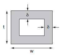
Fig 6 Current flow in shell determined by skin depth
Q16) What is cross stalk? What are the cross-talk delay effects explain in detail?
A16) Cross talk
When wire A switches, it tends to bring its neighbor B along with it on account of capacitive coupling, also called crosstalk. If B is supposed to switch simultaneously, this may increase or decrease the switching delay. If B is not supposed to switch, crosstalk causes noise on B. We will see that the impact of crosstalk depends on the ratio of Cadj to the total capacitance. Note that the load capacitance is included in the total, so for short wires and large loads, the load capacitance dominates and crosstalk is unimportant. Conversely, crosstalk is very important for long wires.
Crosstalk Delay Effects
If both a wire and its neighbor are switching, the direction of the switching affects the amount of charge that must be delivered and the delay of the switching. Table summarizes this effect. The charge delivered to the coupling capacitor is Q = Cadj  V, where
  V is the change in voltage between A and B. If A switches but B does not,
  V = VDD. The total capacitance effectively seen by A is just the capacitance to ground and to B. If both A and B switch in the same direction,
  = 0. Hence, no charge is required and Cadj is effectively absent for delay purposes. If A and B switch in the opposite direction,
  V = 2VDD. Twice as much charge is required. Equivalently, the capacitor can be treated as being effectively twice as large switching through VDD. This is analogous to the Miller effect discussed in Section 4.4.6.6. The Miller Coupling Factor (MCF) describes how the capacitance to adjacent wires is multiplied to find the effective capacitance.
Some designers use MCF = 1.5 as a statistical compromise when estimating propagation delays before layout information is available.
B | V |  | MCF |
Constant |
 |  | 1 |
Switching same direction as A | 0 |  | 0 |
Switching opposite to A |  |  | 2 |
Crosstalk Noise Effects
Suppose wire A switches while B is supposed to remain constant. This introduces noise as B partially switches. We call A the aggressor or perpetrator and B the victim. If the victim is floating, we can model the circuit as a capacitive voltage divider to compute the victim noise, as shown in Figure below  Vaggressor is normally VDD

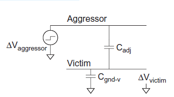
Fig 7 Coupling to floating victim
If the victim is actively driven, the driver will supply current to oppose and reduce the victim noise. We model the drivers as resistors, as shown in Figure below. The peak noise becomes dependent on the time constant ratio k of the aggressor to the victim.
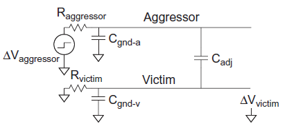
Fig 8 Coupling to driven victim


Q17) Derive the equation for propagation delay in Elmore delay?
A17) According to the Elmore delay model, a gate with effective resistance R and capacitance C has a propagation delay of RC. A wire with distributed resistance R and capacitance C treated as a single π-segment has propagation delay RC/2. Reviewing the properties of RC circuits, we recall that the lumped RC circuit in Figure (a) has a unit step response of

The propagation delay of this circuit is obtained by solving for tpd when Vout(tpd) = 1/2:

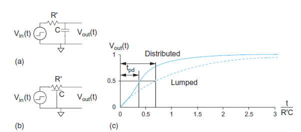
Fig 9 Lumped and Distributed RC circuit Response
The distributed RC circuit in Figure (b) has no closed form time domain response. Because the capacitance is distributed along the circuit rather than all being at the end, you would expect the capacitance to be charged on average through about half the resistance and that the propagation delay should thus be about half as great. A numerical analysis finds that the propagation delay is 0.38R’C.
The Elmore model with the true results for a logic gate, recall that logic gates have complex nonlinear I-V characteristics and are approximated as having an effective resistance. If we characterize that effective resistance as R = R’ ln 2, the propagation delay really becomes the product of the effective resistance and the capacitance: tpd = RC.
For distributed circuits, observe that
0.38 R’C = (1/2) R’C ln 2 = RC/2
Therefore, the Elmore delay model describes distributed delay well if we use an effective wire resistance scaled by ln 2. This suggests that when the input is slow, the effective resistance for delay calculations in a distributed RC circuit is equal to the true resistance.
Q18) What are repeaters and how do they improve the performance of the system. Derive the equation of energy per unit length required to send a bit in a wire?
A18) Repeaters
Both resistance and capacitance increase with wire length l, so the RC delay of a wire increases with l2, as shown in Figure (a). The delay may be reduced by splitting the wire into N segments and inserting an inverter or buffer called a repeater to actively drive the wire, as shown in Figure (b). The new wire involves N segments with RC flight time of (l/N)2, for a total delay of l2 /N. If the number of segments is proportional to the length, the overall delay increases only linearly with l.
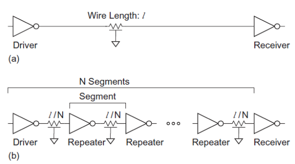
Fig 10 Wire with and without repeaters
Using inverters as repeaters gives best performance. Each repeater adds some delay. If the distance is too great between repeaters, the delay will be dominated by the long wires. If the distance is too small, the delay will be dominated by the large number of inverters. As usual, the best distance between repeaters is a compromise between these extremes. Suppose a unit inverter has resistance R, gate capacitance C and diffusion capacitance Cpinv. A wire has resistance Rw and capacitance Cw per unit length. Consider inserting repeaters of W times unit size.
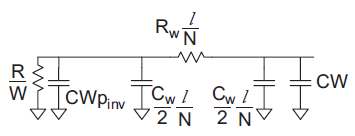
Fig 11 Equivalent circuit for segment of repeated wire
Figure above shows a model of one segment. The Elmore delay of the repeated wire is

Differentiating above equation w.r.t W and N we get

Assuming pinv = 0.5

The delay per unit length of a properly repeated wire is

To achieve this delay, the inverters should use an nMOS transistor width of

The energy per unit length to send a bit depends on the wire and repeater capacitances

In other words, repeaters sized for minimum delay add 87% to the energy of an unrepeated wire.
Q19) Explain the cross talk control scheme?
A19) Cross talk Control
The capacitive crosstalk is proportional to the ratio of coupling capacitance to total capacitance. For modern wires with an aspect ratio (t/w) of 2 or greater, the coupling capacitance can account for 2/3 to 3/4 of the total capacitance and crosstalk can create large amounts of noise and huge data-dependent delay variations.
There are several approaches to controlling this crosstalk:
_ Increase spacing to adjacent lines
_ Shield wires
_ Ensure neighbors switch at different times
_ Crosstalk cancellation
The easiest approach to fix a minor crosstalk problem is to increase the spacing. If the crosstalk is severe, the spacing may have to be increased by more than one full track. In such a case, it is more efficient to shield critical signals with power or ground wires on one or both sides to eliminate coupling. For example, clock wires are usually shielded so that switching neighbors do not affect the delay of the clock wire and introduce clock jitter.
Sensitive analog wires passing near digital signals should also be shielded. An alternative to shielding is to interleave busses that are guaranteed to switch at different times. For example, if bus A switches on the rising edge of the clock and bus B switches on the falling edge of the clock, by interleaving the bits of the two busses you can guarantee that both neighbors are constant during a switching event. This avoids the delay impact of coupling; however, you must still ensure that coupling noise does not exceed noise budgets. Figure below shows wires shielded (a) on one side, (b) on both sides, and (c) interleaved. Critical signals such as clocks or analog voltages can be shielded above and below as well.

Fig 12 Wire Shielding Topologies
Alternatively, wires can be arranged to cancel the effects of crosstalk. Three such methods include staggered repeaters, charge compensation, and twisted differential signaling. Each technique seeks to cause equal amounts of positive and negative crosstalk on the victim, effectively producing zero net crosstalk.
Figure (a) below shows two wires with staggered repeaters. Each segment of the victim sees half of a rising aggressor segment and half of a falling aggressor segment. Although the cancellation is not perfect because of delays along the segments, staggering is a very effective approach. Figure (b) below shows charge compensation in which an inverter and transistor are added between the aggressor and victim. The transistor is connected to behave as a capacitor. When the aggressor rises and couples the victim upward, the inverter falls and couples the victim downward. By choosing an appropriately sized compensation transistor, most of the noise can be cancelled at the expense of the extra circuitry. Figure (c) shows twisted differential signaling in which each signal is routed differentially. The signals are swapped or twisted such that the victim and its complement each see equal coupling from the aggressor and its complement. This approach is expensive in wiring resources, but it effectively eliminates crosstalk.
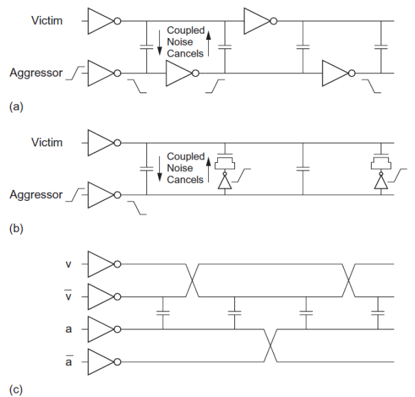
Fig 13 Cross talk Control Scheme
Q20) What device is used instead of repeaters to overcome the drawback of repeaters?
A20) Regenerators
Repeaters are placed in series with wires and thus are limited to unidirectional busses. An alternative is to use regenerators (also called boosters) placed in parallel with wires at periodic intervals, as shown in Figure below. When the wire is initially ‘0,’ the regenerator senses a rising transition and accelerates it. Conversely, when the wire is initially ‘1,’ the regenerator accelerates the falling transition. Regenerators trade off up to 20% better delay or energy for reduced noise margins.
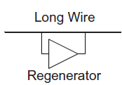
Fig 14 Regenerator
Figure below shows a self-timed regenerator. When the wire begins to rise, the LO-skewed NAND gate detects the transition midway and turns on the pMOS driver to assist. The normal skew inverters eventually detect the transition and flip node x, turning off the pMOS driver. When the wire begins to fall, the HI-skewed NOR gate turns on the nMOS to assist.
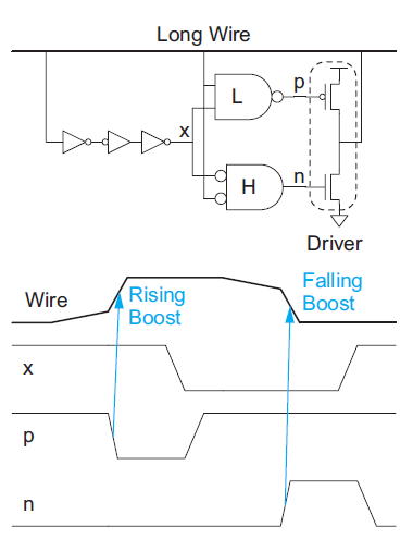
Fig 15 Regenerator