Unit-3
Field Effect Transistor
Q1) For the circuit shown in figure calculate ID , VDS, VG and VS
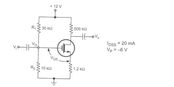 |
A1) Applying KVL to the input circuit.
VGS = VG – VS
= 3 – IS RS
Since VS = IS RS
= 3 – ID RS Since ID = IS
We have
ID = IDSS ( 1 – VGS / VP ) 2
Substituting the value of VGS we get
ID = IDSS ( 1 – (3 – ID RS)/Vp) 2 = 20 x 10 -3 ( 1 – ( 3 – ID x 1.2 x 10 3 / -6)
= 20 x 10 -3 ( 1 – [ (-0.5) + 200 ID ]) 2 = 20 x 10 -3 ( 1.5 -2)
= 20 x 10 -3 (2.25 – 600ID + 40000ID 2)
I D = 0.045 – 12 I D + 800 I D 2
800 I D 2 – 13 I D + 0.045 =0
Solving for quadratic equation we get
= -(-13) ± [ (13) 2 – 4(800)(0.045)] ½ / 2(800)
= 13 ± [ 169 -144] ½ / 1600 = 13 ±  / 1600 = 13 ± 5 /1600 = 5mA or 11.25 mA
If we calculate the value of VDS taking ID = 11.25mA we get
VDS = VDD – ID ( RD + RS)
= 12 – 11.25 x 10 -3 ( 500 + 1.2 x 10 3)
= 12 – 19.125 = -7.125
Practically the value of VDS must be positive hence ID= 11.25 mA is invalid
Hence take ID = 5mA
VDS = VDD – ID (RD + RS) = 12 – 5 x 10 -3 (500 + 1.2 x 10 3) = 12 – 8.5 = 3.5 V
VGS = 3 – ID RS = 3- 5 x 10 -3 x 1.2 x 10 3 = 3 – 6 = -3 V
Vs = ID RS = 5 x 10 -3 x 1.2 x 10 3 = 6V
Q2) Explain transfer characteristics of FET?
A2) The transfer characteristics can be determined by observing different values of drain current with variation in gate-source voltage provided that the drain-source voltage should be constant. The transfer characteristics are just opposite to drain characteristics.
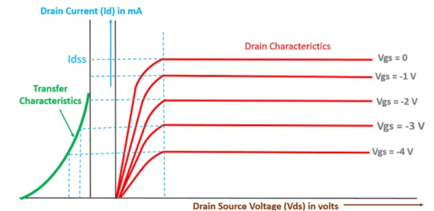 |
Fig 1 Transfer characteristics of N-channel JFET
Q3) What are FET how are they classified?
A3)
- An FET is a three-terminal amplifying device.
- Its terminals are source, gate, and drain, which acts respectively like emitter, base, and collector of a normal transistor.
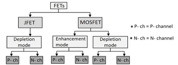
- There are two distinct families of FETs.
- The first is known as ‘junction-gate’ types of FETs or JUGFET or JFET.
- The second family is called ‘insulated-gate’ FETs or Metal Oxide Semiconductor FETs or MOSFET.
- ‘N-channel’ and ‘p-channel’ are the two versions of both types of FET.
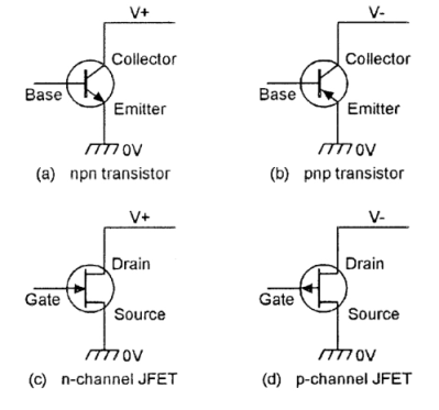 |
Fig 1 Transistor anf JFET
Classification
 |
Q4) Explain Self biasing in FET?
A4) For Self-Biased the figure is shown below. It is the most common method of biasing used. The N-channel JFET is as there is no gate current through reverse biased gate source the gate current IG=0 and VG = IGRG=0. The value of voltage at source will be VS = IDRS
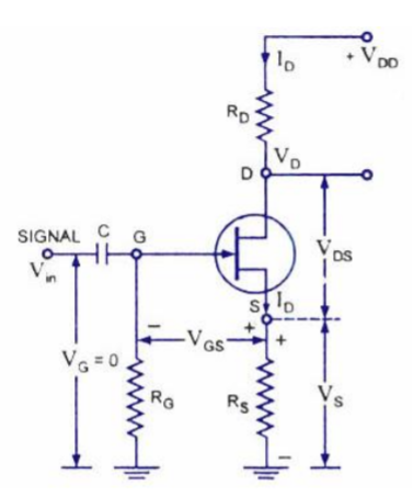 |
Fig 3 Self Biased FET
The equation for VGS is given as
VGS = VG-VS =0-IDRS = -IDRL
The self-biasing of a JFET stabilizes its Q-point against any change in its parameters like transconductance.
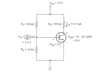
Q5) For the circuit shown in figure assume that R1 = 30KΩ and R2 = 10 KΩ. Rd = 40KΩ . Vdd = 10V and VT=1V , Vgs = 2V and K = 0.1mA /V2 . Find Id and VDS
|
A5) VG = VGS = (R2/R1+R2) VDD = (10/10+30) (10) = 2.5V
Assuming that the MOSFET is biased in the saturation region the drain current is
VDS = VDD – ID RD = 10 – (0.1)(40) = 6V.
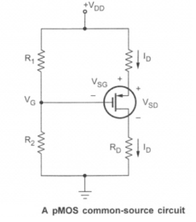 |
Here, the source is tied to +VDD, Which, become signal ground in the a.c. Equivalent circuit. Thus, it is also a common-source circuit.
The d.c. Analysis for this circuit is essentially the same as for the n-channel MOSFET circuit. The gate voltage is given by,
VG = (R2/R1 + R2) (VDD)
And the source to gate voltage is given by
VSG = VDD -VG
Assuming VGS <VT or VSG > |VT| the device in the saturation region and the drain current is given by
ID = K(VSG + VT) 2
And the source to drain voltage is given by
VSD = VDD – ID RD
If VSD > VSD (sat) then MOSFET is in saturation region.
IF VSD < VSD(sat) MOSFET is in non-saturation region.
Q6) Explain common drain amplifiers?
A6)A common-drain JFET amplifier is one in which the input signal is applied to the gate and the output is taken from the source, making the drain common to both. Because it is common, there is no need for a drain resistor. A common-drain JFET amplifier is shown in Figure below. A common-drain amplifier is also called a source-follower. Self-biasing is used in this particular circuit. The input signal is applied to the gate through a coupling capacitor, C1, and the output signal is coupled to the load resistor through C2
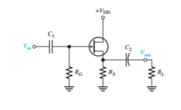 |
Fig 5 Self Biased CD amplifier
The expression for voltage gain will be
AV = 
AV = 
The gain is always<1. The RG is in parallel with RIN at gate so, the total input resistance is
Rin = RG||RIN (gate)
Q7) Explain common source amplifiers?
A7) In CS amplifier the ac input is applied to gate and the output is taken across drain. This configuration has a bypass source resistor which connects the source to the ground. The below figure is shown of a self-biased common source n-channel JFET amplifier which is capacitively coupled. The resistor RG keeps gate at 0V and prevents loading of ac signal source.
The capacitor C2 keeps the source of JFET at ac ground. The gate source voltage swing between VGSQ above and below its Q-point and causing swig in drain current too. The voltage drop across RD increases as the drain current increases. The VDS is 1800 out of phase with VGS.
The figure below shows sinusoidal variation VGS produces corresponding sinusoidal variation in ID. The value of VGS swings to more negative value of Q-point ID decreases from its Q-point. The value of ID increases when VGS swings to a less negative value. The signal at the gate drives the drain current above and below the Q-point on the load line.
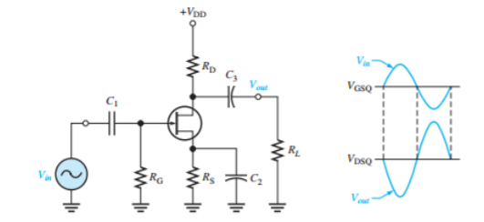 |
Fig 6 Self-Biased CS amplifier
Lines projected from the peaks of the gate voltage across to the ID axis and down to the VDS axis indicate the peak-to-peak variations of the drain current and drain-to-source voltage, as shown. Because the transfer characteristic curve is nonlinear, the output will have some distortion. This can be minimized if the signal swings over a limited portion of the load line.
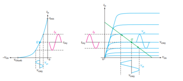 |
Fig 7 Transfer characteristics for CS amplifier
The ac equivalent circuit is shown below. The input resistance to JFET is very high so all of the input voltage from the signal source appears at the gate with small drop across internal source resistance.
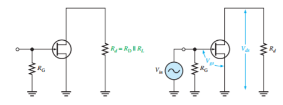 |
Fig 8 AC equivalent Circuit
Vgs = Vin
The voltage gain will be Av = gmRd
The input which is actually seen by signal source is RG in parallel with FET input resistance VGS IGSS.
Rin = RG||(VGS/IGSS)
Q8) Explain Common gate amplifiers?
A8) A self-biased common-gate amplifier is shown in figure. The gate is connected directly to ground. The input signal is applied at the source terminal through C1. The output is coupled through C2 from the drain terminal.
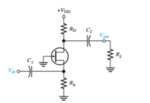 |
Fig 9 Common gate amplifier
The voltage gain is given by
Av =  =
=  =
=  = AV =
Rd = RD||RL
The input current is given by
Vin = Vgs
The input resistance at the source terminal is
Rin=  =
= 
Rin = 1/gm
Q9) Draw the circuit for potential divider bias for JFET?
A9) The Potential Divider Bias for JFET is shown below. The resistors RG1 and RG2 form potential divider across VDD. The voltage V2 across RG2 provides necessary bias. The gate is reverse bias and IG=0.
VG = V2= (VDD/RG1*RG2) *RG2
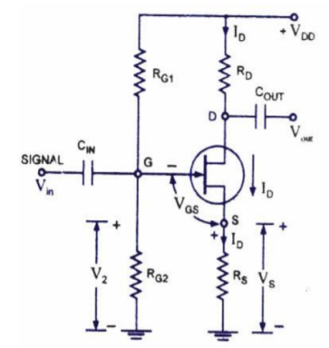 |
Fig 10 Potential Divider Bias Circuit
The operating point will be
ID = (V2-VGS)/RS
VDS = VDD-ID(RD+RS)
Q10) Explain FET small signal model?
A10) As we know FET provide high input impedance and is an excellent amplifier with voltage gain. The small signal low frequency model is shown below for n-channel JFET. From below figure we can understand that the input impedance is represented by open circuit and hence IG= 0. The resistance rd represents the output impedance.
The gate to source voltage only controls the drain to source current for JEFT. The transconductance factor gm is
 Id = gm
 VGS
VGS
The equation for output impedance rd is
rd =  |for VGS constant