Unit 3
DSBSC
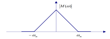
Q1) Consider a message signal m(t) with spectrum shown below. The message bandwidth is wm = 2∏ * 103 rad/sec. This signal is applied to a product modulator, together with a carrier wave , Ac cos(ωc*t) producing the DSB-SC modulated signal s(t). The modulated signal is next applied to a coherent detector. Assuming perfect synchronism between the carrier waves in the modulator and detector, determine the spectrum of the detector output when :
A1)
(a) The carrier frequency ωc =2.5∏ * 103 rad/sec.
(b) The carrier frequency. ωc =1.5 π × 103 rad/sec
What is the lowest carrier frequency for which each component of the modulated signal s(t) is uniquely determined by m(t) ?
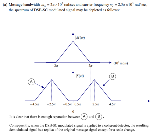
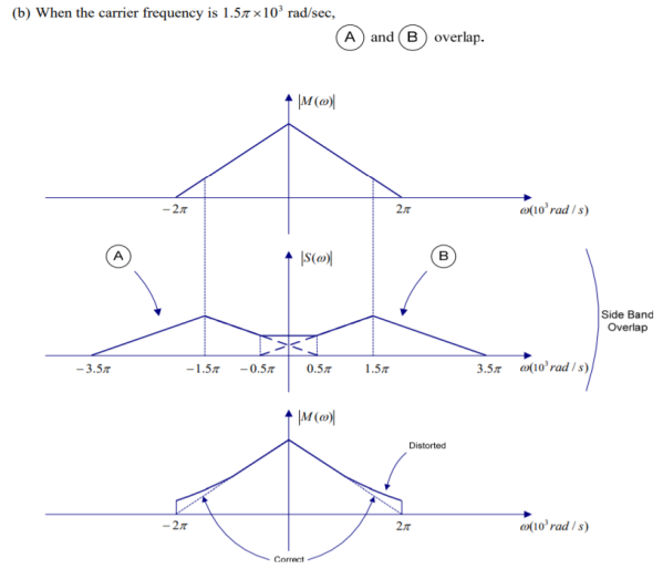
The spectrum of demodulated signal appears at the output of the detector.
There is a distortion in the message signal.
To avoid this, we must choose the carrier frequency in accordance with the condition ωc ≥ ω m .
The minimum acceptable value of ωc is therefore ω m For ωc < ω m , we have sideband overlap and therefore message distortion.
Q2) A modulating signal m(t)=10cos(2π×103t)m(t) is amplitude modulated with a carrier signal c(t)=50cos(2π×105t). Find the modulation index, the carrier power, and the power required for transmitting AM wave.
A2)
Given, the equation of modulating signal as
m(t)=10 cos(2π×103t) m(t)
We know the standard equation of modulating signal as
m(t)=Am cos(2πfmt) m(t)
By comparing the above two equations, we will get
Am=10 volts
And Frequency of modulating signal as
Fm=103Hz=1KHz
Given, the equation of carrier signal is
c(t)=50 cos(2π×105t))
The standard equation of carrier signal is
c(t)=Ac cos(2πfct) c(t)
By comparing these two equations, we will get
Amplitude of carrier signal as Ac=50 volts
And Frequency of carrier signal as fc=105Hz=100KHz
We know the formula for modulation index as
μ=Am/Ac
μ=10/50=0.2
Therefore, the value of modulation index is 0.2 and percentage of modulation is 20%.
The formula for Carrier power, Pc
Pc=Ac2 /2R
Assume R=1ΩR=1Ω and substitute Ac value in the above formula.
Pc=(50)2/2(1)=1250W
Therefore, the Carrier power, Pc is 1250 watts.
We know the formula for power required for transmitting AM wave is
Pt=Pc(1+μ2/2)
Pt=1250(1+(0.2)22)=1275W
Therefore, the power required for transmitting AM wave is 1275 watts.
Q3) Explain Frequency Discrimination Method.
A3)
In this method the DSB signal is passed through band pass filter to generate SSB signal.
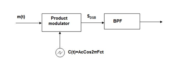
Fig. Frequency Discrimination method
The center frequency of the band pass signal decides whether USB or LSB signal is generated.
Suppose we want to transmit USB then using band pass filter with center frequency fc + w/2 we obtain the desired result as shown in the figure.
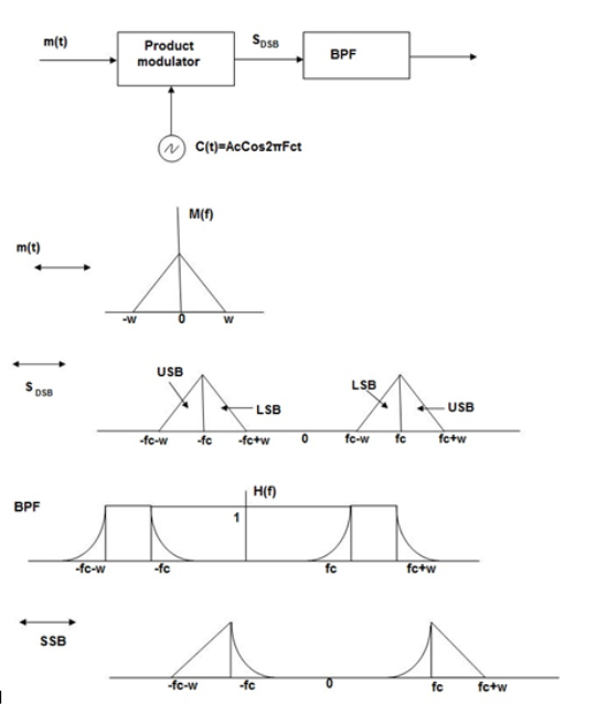
Fig.: Resultant output
Q4) Describe Phase Discriminated Method.
A4)
Consider the following block diagram of SSB-SC modulator using phase discrimination method.
.
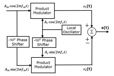
Fig. Phase Discriminated Method
- It consists of two product modulators, two −900 phase shifters, one local oscillator and one summer block.
- The product modulator produces an output, which is the product of two inputs.
- The −900 phase shifter produces an output, which has a phase lag of −900 with respect to the input.
- The local oscillator is used to generate the carrier signal.
- Summer block produces an output, which is either the sum of two inputs or the difference of two inputs based on the polarity of inputs.
Q5) Compare Power Calculations of SSB-SC and DSB-SC.
A5)
SSBSC Wave
Consider the following equation of SSBSC modulated wave.
s(t)=Am Ac/2 cos[2π(fc+fm)t] for the upper sideband
Or
s(t)=Am Ac/2 cos[2π(fc−fm)t]for the lower sideband
Power of SSB-SC wave is equal to the power of any one sideband frequency components.
Pt=PUSB=PLSB
We know power
P=Vrms2 / R
=(vm/√2)2 / R
In this case, the power of the upper sideband is
PUSB=(AmAc/2√2)2 / R = Am2Ac2 /8R.
Similarly, for lower sideband power.
PLSB=Am2Ac2 / 8R
Therefore, the power of SSB-SC wave is
Pt=Am2Ac2 / 8R
DSBSC Wave
Consider the following equation of DSBSC modulated wave.
s(t)=AmAc2cos[2π(fc+fm)t]+AmAc2cos[2π(fc−fm)t]
Power of DSBSC wave is equal to the sum of powers of upper sideband and lower sideband frequency components.
Pt=PUSB+PLSB
We know the standard formula for power of cos signal is
P=vrms2 /R=(vm√2)2 /R
First, let us find the powers of upper sideband and lower sideband one by one.
Upper sideband power
PUSB=(AmAc/2√2)2/R=Am2Ac2 / 8R
Similarly, we will get the lower sideband power same as that of upper sideband power.
PLSB=Am2Ac2/8R
Now, let us add these two sideband powers in order to get the power of DSBSC wave.
Pt=Am2Ac2 /8R+Am2Ac2/8R
Pt=Am2Ac2 /4R
Therefore, the power required for transmitting DSBSC wave is equal to the power of both the sidebands.
Q6) Explain generation of DSBSC by Balanced Modulator (Product Modulator).
A6)
A balanced modulator consists of two standard amplitude modulators arranged in a balanced configuration so as to suppress the carrier wave as shown in the following block diagram. It is assumed that the AM modulators are identical, except for the sign reversal of the modulating wave applied to the input of one of them. Thus, the output of the two modulators may be expressed as,
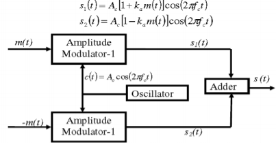
Fig.: Balanced Modulator
Subtracting s2(t) from s1(t) we get
s(t) = s1(t) – s2(t)
s(t) = 2 ka m(t) cos(2πfct)
Hence, except for the scaling factor 2ka, the balanced modulator output is equal to the product of the modulating wave and the carrier.
Q7) Explain generation of DSBSC by Ring Modulator.
A7)
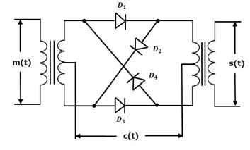
Fig.: Ring Modulator
Operation
- In this diagram, the four diodes D1,D2,D3 and D4 are connected in the ring structure. Hence, this modulator is called as the ring modulator.
- Two center tapped transformers are used in this diagram. The message signal m(t) is applied to the input transformer, whereas, the carrier signals c(t) is applied between the two center tapped transformers.
- During the positive half cycle of the carrier signal, the diodes D1 and D3 are switched ON and the other two diodes D2 and D4 are switched OFF.
- In this case, the message signal is multiplied by +1.
- During the negative half cycle of the carrier signal, the diodes D2 and D4 are switched ON and the other two diodes D1 and D3 are switched OFF.
- In this case, the message signal is multiplied by -1. This results in 1800 phase shift in the resulting DSBSC wave.
From the above analysis, we can say that the four diodes D1, D2, D3 and D4 are controlled by the carrier signal.
If the carrier is a square wave, then the Fourier series representation of c(t) is given by
c(t) = 4 / π  n-1 / 2n -1 cos[2πfct(2n−1)]
We will get DSBSC wave s(t) which is just the product of the carrier signal c(t)) and the message signal m(t) i.e.,
s(t) = 4 / π  n-1 / 2n -1 cos[2πfct(2n−1)] m(t)
the ring modulator.
DSBSC modulators are known as product modulators as they produce the output, which is the product of two input signals.
Q8) Explain SSBSC in detail.
A8)
The process of suppressing one of the sidebands along with the carrier and transmitting a single sideband is called as Single Sideband Suppressed Carrier system or simply SSBSC. It is plotted as shown in the following figure.
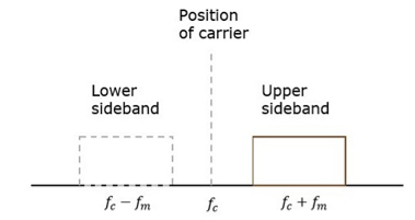
Fig. SSB
Carrier and sideband are suppressed and single sideband is allowed for transmission.
Let us consider the
Modulating signal
m(t)=Am cos(2πfmt)
Carrier signal
c(t)=Ac cos(2πfct)
Mathematically, we can represent the equation of SSB-SC wave as
s(t)=AmAc2cos[2π(fc+fm)t] for the upper sideband
Or
s(t)= AmAc2cos[2π(fc−fm)t] for the lower sideband