Unit - 1
PN Junction Diode
Q1) What is depletion layer? Explain using PN junction diode.
A1)
When a semi-conductor is doped such that half the portion is doped with the trivalent impurity (Al, Ar, Bi) and the other half is doped with pentavalent impurity (B, P) then the junction formed is known as PN junction.

Its symbol is

Depletion layer
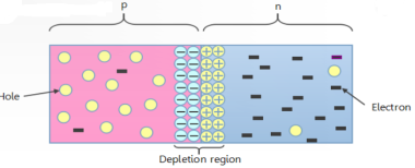
At normal condition, the holes from P region diffuse into N region and electrons from N region diffuse in P region.
A thin layer of positive ion is formed in the N region and negative ions in the P region near the junction are formed.
This thin layer that is formed is known as depletion layer.
Q2) Draw and explain reverse biasing.
A2)
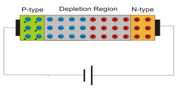
When positive terminal is connected to the n-type region and the negative terminal is connected to the p-type region then the pn junction is said to be in reverse biased condition.
When no voltage applied across the p n junction, the potential developed across the junction is 0.3 volts at 25oC for germanium and 0.7 volts at 25oC for silicon p n junction.
The polarity of this potential barrier is same as the polarity of voltage source applied during reverse biased condition.
Now if reverse biased voltage is increased the barrier potential developed also increases. Hence, the pn junction widens.
The free electrons of the n-type region are attracted towards positive terminal of the source because of that more positive impurity ions are created in the depletion layer which makes the layer thicker.
At the same time, electrons are injected in the p-type region. Due to the positive potential of the n-type region the electrons are drifted towards the junction and combine with holes and create more positive impurity ions in the layer.
Q3) Draw and explain I-V characteristics of PN junction diode.
A3)
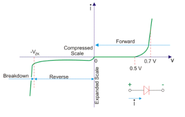
In the forward bias, the operational region is in the first quadrant.
The threshold voltage for Germanium is 0.3 V and for Silicon is 0.7 V.
Beyond this, the graph goes upward in a non linear manner.
This graph is for the dynamic Resistance of the junction in the forward bias.
Q4) Explain types of capacitances in detail.
A4)
Diode Capacitance
The ability of the material to store electric charge is called capacitance.
The change of capacitance at the depletion region can be defined as the change in electric charge per change in voltage.
CT = dQ / dV
Where,
CT = Transition capacitance
DQ = Change in electric charge
DV = Change in voltage
Transition Capacitance
The amount of capacitance changes with increase in voltage is called transition capacitance.
The transition capacitance is also known as depletion region capacitance, junction capacitance or barrier capacitance. Transition capacitance is denoted as CT.
The transition capacitance can be mathematically written as,
CT = ε A / W
Where,
ε = Permittivity of the semiconductor
A = Area of plates or p-type and n-type regions
W = Width of depletion region
Diffusion capacitance (CD)
It occurs in a forward biased p-n junction diode.
It is also referred as storage capacitance. It is denoted as CD.
Diffusion capacitance is given by,
CD = dQ / dV
Where,
CD = Diffusion capacitance
DQ = Change in number of minority carriers stored outside the depletion region
DV = Change in voltage applied across diode
Q5) Draw and explain Zener diode in detail.
A5)
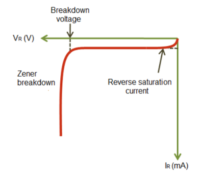
A zener diode is a special type of device designed to operate in the zener breakdown region.
It acts like normal p-n junction diode under forward bias condition. When forward biased voltage is applied, it allows large amount of electric current and blocks only a small amount.
It is heavily doped than the normal p-n junction diode. Hence, it has very thin depletion region. Hence, allows more electric current than the normal p-n junction diodes.
It allows electric current in the reverse direction if the applied reverse voltage is greater than the zener voltage.
It is always connected in reverse direction because it is specifically designed to work in reverse direction.
Symbol

V-I characteristics
Q6) Write short note on photo diode.
A6)
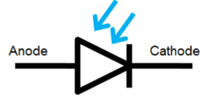
A photodiode is a p-n junction or pin semiconductor device that consumes light energy to generate electric current. It is also sometimes referred as photo-detector, photo-sensor, or light detector.
Photodiodes are specially designed to operate in reverse bias condition. Reverse bias means that the p-side of the photodiode is connected to the negative terminal of the battery and n-side is connected to the positive terminal of the battery.
Photodiode is very sensitive to light so when light or photons falls on the photodiode it easily converts light into electric current. Solar cell is also known as large area photodiode because it converts solar energy or light energy into electric energy.
Symbol
Q7) Draw and explain LED in detail.
A7)
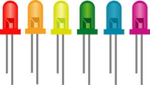
Light Emitting Diodes (LEDs) are the most widely used semiconductor diodes.
It emits either visible light or invisible infrared light when forward biased.
It is an optical semiconductor device that emits light when voltage is applied. It converts electrical energy into light energy.
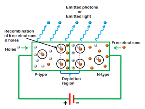
When LED is forward biased, free electrons in the conduction band recombines with the holes in the valence band and releases energy in the form of light.
The process of emitting light in response to the strong electric field or flow of electric current is called electroluminescence.
It works only in forward bias condition. When LED is forward biased, the free electrons from n-side and the holes from p-side are pushed towards the junction.
When free electrons reach the junction or depletion region, some of the free electrons recombine with the holes in the positive ions.
The current flowing through the LED is mathematically written as

Where,
IF = Forward current
VS = Source voltage or supply voltage
VD = Voltage drop across LED
RS = Resistor or current limiting resistor
Symbol
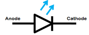
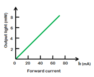
Output characteristics of LED
