Unit - 3
BJT Introduction
Q1) Determine the values of VCC RC and RB of a fixed bias configuration for a given load line and defined Q point.
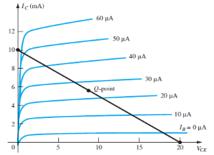
A1)


Q2) Determine dc bias voltage VCE and current IC for voltage divider configuration.
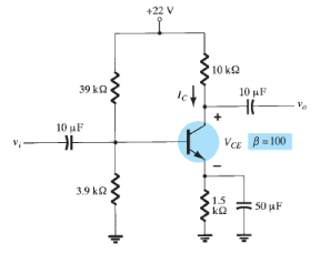
A2)


Q3) Explain operation of PNP and NPN in detail.
A3)
- The operation is explained by considering the PNP transistor. The operation of NPN transistor varies with a little exchange of roles played by the electrons and holes.
- Now, there is a reduction in the width of the depletion layer due to the applied bias which results in a heavy flow of majority carriers from p to n type material.
- On removing the base emitter bias of pnp transistor we get forward biasing of transistor.
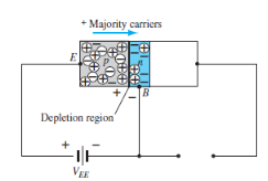
Fig: Forward bias of pnp transistor
- Now if the flow of majority carrier is zero then the flow of minority carrier leads to reverse bias condition.
- When both the biasing potentials are applied simultaneously then both the majority and minority carriers start flowing.
- Here the n type material is very small and has less conductivity hence the magnitude of base current is of the order of microamperes
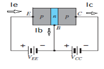
Fig.: pnp transistor
- Now applying Kirchoff’s law we get
Ie = Ic + Ib
- Hence, the emitter current is sum of the collector current and base current.
- The collector current has two components : the majority (Icm) and minority currents (Ico).
Ic = Icm + Ico
- Ico is known as the leakage current and is measured in micro or nano amperes.
- It is temperature sensitive and can affect the stability of the system with high temperature requirement if not considered properly.
Q4) Explain various regions in common emitter configuration.
A4)
The notation and symbols of npn and pnp transistors are given below:
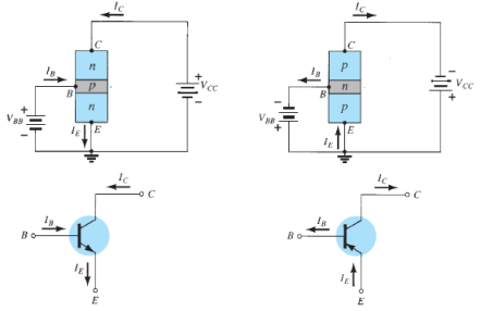
Fig. : NPN CE and PNP CE
In the above figure all the currents are shown in their actual conventional directions.
The current relation developed earlier is still applicable,
IE = IB + IC
Where IE , IB , IC are the collector, base and emitter currents respectively.
The graphical symbol of the PNP common emitter configuration is
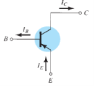
Fig.: PNP common emitter
Now, to study the behavior of the device we require two characteristics:
Input Characteristic Curve
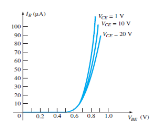
Fig.: Input Characteristic Curve
It is the graph between the input current IB to the input voltage VBE for a range of values of output voltage VCE.
Note that the magnitude IB of is in micro amperes and that of IC is in milli amperes.
Output Characteristic Curve
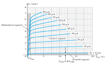
Fig.: Output Characteristic Curve
It is the graph between the output current IC to the output voltage VCE for a range of values of input current IB.
It has three basic regions:
Active Region
- Here, the base-emitter junction is forward biased and collector base junction is reverse biased.
- These are the same conditions that existed in the active region of the common base configuration.
- This can be employed for voltage, current or power amplification.
Cut-off Region
- Here IC is not equal to zero when IB is zero.
- For linear amplification purposes, it is defined as IC = ICEO .
- The region below IB = 0µA is to be avoided for undistorted output signal.
- When the transistor is used as a switch, the condition should be ideally IC = 0mA for a chosen VCE voltage.
Saturation Region
- It is the region that lies towards the left of VCE = 0V.
Q5) What is a voltage divider bias? Explain.
A5)
In the previous configurations, the bias current and the collector emitter voltage were a function of current gain β of a transistor.
Since β is temperature sensitive, actual value could not be defined.
Hence it is very much desired to develop a bias circuit which is independent of β.
This gives a Voltage divider configuration.
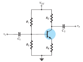
Fig.: Voltage Divider Bias
When analysed on exact basis, the sensitivity to changes in β is very small and if circuit parameters are nicely chosen then it can even become independent of β.
IB changes with the change in β but the operating point on the characteristics defined by Ic and Vce remain fixed if proper parameters are employed.
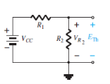
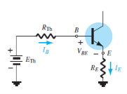
Applying exact analysis, the above circuit is redrawn as,
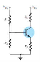
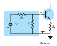
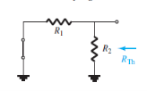
Fig.: Analysis of Voltage Divider circuit (Ref. 2)
The voltage is replaced by a short circuit equivalent (Ref. 2)

Now calculating open circuit thevenin’s voltage and applying voltage divider rule we have (Ref. 2)

Applying kirchoff’s voltage law , (Ref. 2)

Put IE = ( β + 1 ) IB

Once IB is determined then rest of the quantities can be found out (Ref. 2)

The remaining equations for collector, emitter and base voltages are same as obtained for emitter- bias configuration.
Q6) Explain DC Load line.
A6)
- The load line solution was found by superimposing the actual characteristics on a plot of network equation involving the same network variables.
- It is known as load line analysis as load of network defined the slope of the straight line connecting the points defined by network parameters.
- The smaller the load resistance, the steeper the slope of the network load line.
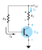
Fig.: DC Load Line (Ref. 2)
- The output equation is given by,

- The characteristic curve is drawn as
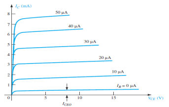
Fig.: DC Load Line characteristic curve (Ref. 2)


- If we choose VCE = 0V then,


Q7) In a common base connection, current amplification factor is 0.9. If the emitter current is 1mA, determine the value of base current.
A7)
Here, α = 0.9, IE = 1 mA
Now 
Or 
Also 

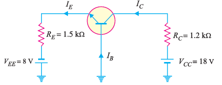
Q8) For the common base circuit shown in Fig., determine IC and VCB. Assume the transistor to be of silicon.
A8)
Since the transistor is of silicon, VBE = 0.7V.
Applying Kirchhoff’s voltage law to the emitter-side loop,we get,

Or 


Applying Kirchhoff’s voltage law to the collector-side loop, we have,


Q9) Find the value of β if (i) α = 0.9 (ii) α = 0.98 (iii) α = 0.99.
A9)
(i) α = 0.9

(ii) α = 0.98

(iii) α = 0.99
