Unit - 4
FET
Q1) Draw and explain the I-V characteristics of FET.
A1)
Output Characteristics or Drain Characteristics
In the absence of external bias: In this case, as there is no voltage between gate and source terminal, thus, the drain current will flow from drain terminal to source terminal. We have already discussed in the working of JFET that majority charge carriers flow from source to drain and as a consequence of which the current flows from drain to source.
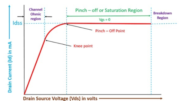
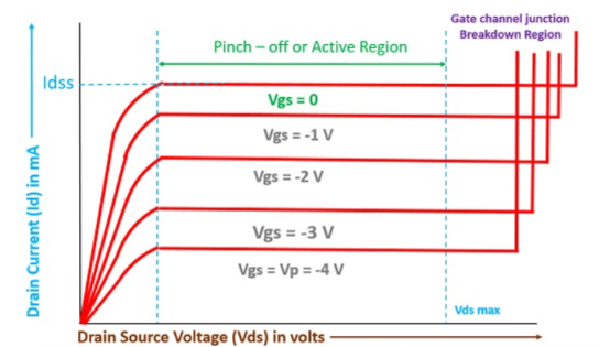
With external bias: When the external bias is applied to the gate-source terminal, the gate-source terminal becomes reversed bias externally. Obviously, if we are supplying an external voltage, then we can achieve the pinch-off point quite early as compared to the circuit which is not biased.
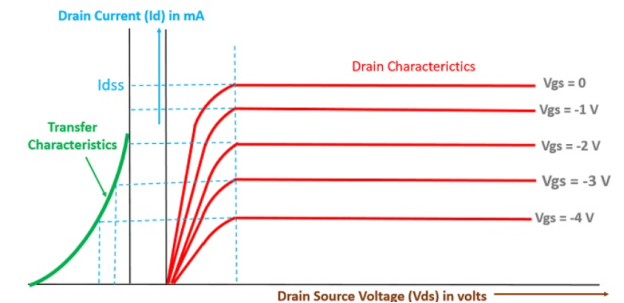
Transfer Characteristics
The transfer characteristics can be determined by observing different values of drain current with variation in gate-source voltage provided that the drain-source voltage should be constant. The transfer characteristics are just opposite to drain characteristics.
Q2) Define Transconductance and amplification factor of FET.
A2)
Transconductance is defined as the ratio of change in drain current (δID) to change in the gate to source voltage (δVGS) with a constant drain to source voltage (VDS = Constant).

Amplification Factor
It is defined as the ratio of change of drain voltage (δVDS) to change of gate voltage (δVGS) at a constant drain current (ID = Constant).
 There is a relation between transconductance (gm) and dynamic output resistance (rd) and is given as.


Q3) Explain JFET amplifier in detail.
A3)
- Small signal amplifiers are made using Field Effect Transistors. They have extremely high input impedance along with a low noise output making them ideal for use in amplifier circuits that have a very small input signal.
- The design of an amplifier circuit is based on the same principle as that for the bipolar transistor circuit used for a Class A amplifier.
- Firstly, a suitable quiescent point or “Q-point” is found for the correct biasing of the JFET amplifier circuit with single amplifier configurations of Common-source (CS), Common-drain (CD) or Source-follower (SF) and the Common-gate (CG).
- These three JFET amplifier configurations corresponds to the common-emitter, emitter-follower and the common-base configurations using bipolar transistors.
Construction:
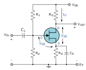
- It consists of an N-channel JFET.
- The JFET gate voltage Vg is biased through the potential divider network made by resistors R1 and R2 and its biasing is done within its saturation region.
- JFET takes no input gate current and allows the gate to be treated as an open circuit.
- Hence, no input characteristics curves are required.
- In order to keep the gate-source junction reverse biased, the source voltage, Vs is made higher than the gate voltage, Vg.

- This source voltage is therefore given as:

- Then the Drain current, Id is also equal to the Source current, given as:

- Resistor, Rs and the source by-pass capacitor, Cs serve the same function as the emitter resistor and capacitor in the common emitter bipolar transistor amplifier circuit to provide good stability and prevent a reduction in the loss of the voltage gain.
- The characteristics of a Common Source JFET Amplifier are similar to the common emitter amplifier.
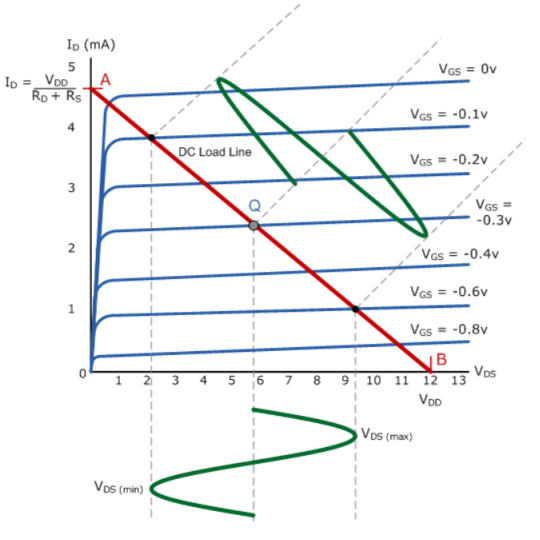
- The actual position of the Q-point is at the mid center point of the load line and is determined by the mean value of Vg.
- The output of the Common Source JFET Amplifier is 180o out of phase with the input signal.
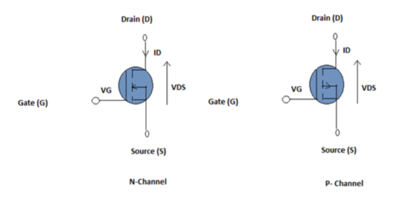
Q4) Write and explain the two modes of MOSFET.
A4)
Depletion Mode
When there is no voltage on the gate, the channel shows maximum conductance. When the voltage on the gate is either positive or negative, the channel conductivity decreases.
Enhancement Mode
The device does not conduct when there is no voltage on the gate. As the voltage increases on the gate, the better the device can conduct.
Q5) Explain the working of MOSFET.
A5)
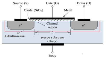
- The aim of the MOSFET is to be able to control the voltage and current flow between the source and drain. It works like a switch.
- The working depends upon the MOS capacitor.
- The MOS capacitor is the main part of MOSFET.
- The semiconductor surface at the below oxide layer is located between source and drain terminal. It can be inverted from p-type to n-type by applying positive or negative gate voltages respectively.
- When the positive gate voltage is applied, the holes present under the oxide layer repel with a repulsive force and holes are pushed downward with the substrate.
- The depletion region populated by the negative charges is the acceptor atoms. The positive voltage also attracts electrons. Now, if a voltage is applied between the drain and source, the current flows between the source and drain and the gate voltage controls the electrons in the channel.
Q6) Define: Gate Cut Off Voltage and Shorted Gate Drain Current
A6)
Gate Cut Off Voltage
At a fixed drain voltage, the drain current (ID) of a JFET depends on the gate to source voltage (VGS). If the gate to source voltage decreases in n channel JFET, the drain current also gets decreased accordingly.
The relation between gate to source voltage and drain current is given by

Shorted Gate Drain Current
When (VGS = 0) and positive drain to source voltage (VDS) is being increased slowly, the drain current gets increased linearly. But after pinch-off voltage (Vp), the drain current increases and gets a constant value. This is the maximum drain current that flows through the channel and is called shorted gated drain current and denoted by IDSS.