Unit - 5
Integrated Circuits
Q1) Draw and explain block diagram of op-amp.
A1)

Fig: Block diagram
The block diagram of op-amp consists of:
- Types of inputs
Non-inverting input
Inverting input
- Input stage
It has a dual input.
It is a differential amplifier which provides balanced output.
It provides voltage gain.
Establishes input resistance of op-amp.
- Intermediate stage
It also has a dual input.
It is a differential amplifier which provides unbalanced output.
The output of the input stage becomes input for the intermediate stage.
Due to direct coupling, the dc voltage is well above 0V.
- Level shifting stage
The output of the intermediate stage becomes input for the level shifting stage.
It is an emitter follower with constant current source.
It is used to shift dc level at the output to 0V wrto ground.
- Output stage
This is the final stage.
It’s a push pull amplifier.
It raises swing in output voltage as well as increases current supply capability of op-amp.
Q2) Write some characteristics of op-amp.
A2)
It has the following characteristics:
- Infinite input resistance [Ri =∞]
- Zero output resistance [RO = 0]
- Infinite voltage gain [AV = ∞]
- Infinite bandwidth [BW = ∞]
- Infinite Common Mode Rejection Ratio
- Infinite slew rate
- Zero offset [ ie,V1 = V2 , VO =0]
- The above characteristics do not change with the change in temperature.
Q3) Draw and explain inverting amplifier.
A3)
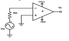
Fig: Inverting op-amp
- As seen in the above figure, input is applied to only one terminal i.e. inverting input terminal.
- The other input terminal is supplied 0V i.e. grounded.
- Hence,
V1 = 0V and V2 = Vin
- Therefore output voltage Vout is given by,
- Vout = A( - Vin )
- Where, A is the voltage gain of op-amp.
- The negative sign implies that the output voltage is 1800 out of phase w.r.to the input voltage.
- Hence, the inverting amplifier amplifies the input signal by voltage gain A and inverts it at the output.
Q4) Draw and explain summing amplifier.
A4)
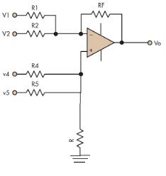
Fig.: Summing amplifier
- In the above figure, each terminal is connected with two input sources through resistors. V1 and V2 is connected to the inverting terminal and V4 and V5 is connected to the non-inverting terminal.
- Assuming R1=R2=R4=R5=RF=R.
- Now, on applying superposition theorem, for finding output voltage due to V1 alone, keep V2=V4=V5=0V.
- Hence, now the circuit acts as an inverting amplifier.
- Therefore,

- Similarly,

- Now, for V4, voltages V1=V2=V5=0V then the circuit behaves as a non-inverting amplifier.


Hence,


Similarly,

So, the resultant output voltage by all the 4 input voltages is given by,
Vo = V01 + V02 + V04 +V05
Vo = -V1 – V2 +V4 + V5
The output voltage Vo is equivalent to the sum all input voltages applied at both the terminals.
Q5) In a summing amplifier, if R = 1kΩ, Va = +3V, Vb = +8V, Vc = +9V, Vd = +5V and supply voltage is ±15V. Find the output voltage Vo.
A5)
Vo = Sum of all input voltages applied at both the terminals
Vo = Va + Vb + Vc +Vd
Vo = -3 -8 +9 +5
Vo = +3V
Q6) Find the output voltage for the given circuit diagram if Rf = 5kΩ.
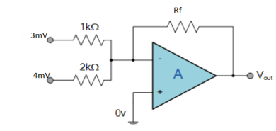
A6)
We know,
Gain (Av) = =
= 
Hence,
Av1 = 
Av2 = 
Now, Output voltage Vo = Sum of the two amplified input signals
Vo = Av1 x V1 + Av2 x V2
Vo =(-5 x 3) + ( -2.5x 4) mV
Vo = -25mV
As the above output voltage is negative hence it is an inverting amplifier.
Q7) Draw and explain Differentiator in detail.
A7)
- A differentiator is a circuit that performs differentiation operation. Hence, the output is a derivative of input.
- In an inverting amplifier, if input resistor is replaced by a capacitor then a differentiator circuit is formed.
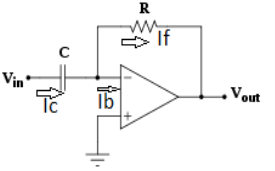
Fig: Differentiator
- In the above fig. On applying Kirchoff’s law we get,

Since Ib = 0 then,
Ic ≈ If

Since Gain A is very large hence, V1 = 0

Or 
- So, the output voltage is RC times the negative rate of change of input voltage.
- When input is a cosine wave, output is a sine wave i.e. it performs the inverse function of integrator circuit.
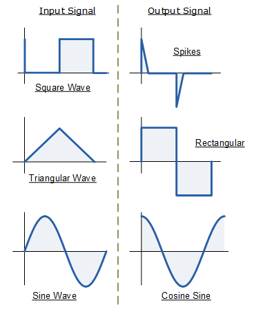
Fig.: Input and output waveform of differentiator
- Frequency response of basic differentiator circuit is given by,
 ( for 0 db gain)