Unit - 3
Semiconductor
Q1) Explain Polycrystalline and Amorphous materials.
A1)
Polycrystalline:
The ordinary hard shape of an element or compound is polycrystalline. As the given name suggest a polycrystalline solid or polycrystal is made up of numerous crystals. The properties of a polycrystal are outstandingly unusual from those of a single crystal. The individual section crystallites are repeatedly referred to as grains and the junctions between these grains are known as grain boundaries. The range of grain varies according to the circumstances in which it is formed. Galvanized steel has a zinc coating with clearly large grains. Other materials have much finer grains.
Amorphous
In materials science, an amorphous or non-crystalline solid is a solid that lacks the long-range order that is the feature of a crystal. At present, "glassy solid" or "amorphous solid" is considered to be the overarching theory, and glass the added out of the ordinary case: Glass is an amorphous solid that exhibits a glass transition. Polymers are repeatedly amorphous. Further types of amorphous solids comprise gels, thin films, and nanostructured materials such as glass. Amorphous metals have low toughness, but high strength.
Q2) What is Fermi – Dirac Distribution? Derive expression for the same.
A2)
The equation for f(E) is called the Fermi-Dirac probability function, and specifies the tiny proportion of all states at energy E (electron volts) engaged in conditions of thermal equilibrium,
f (E) =  ………(1)
Where K= Boltzmann constant, ev/
T = temperature, ,
, =Fermi level for the crystal,ev
The Fermi level represents the energy state with a 50 percent probability of being packed if no forbidden band exists. If E= , then f (E) =
  at all values of temperature. A plot of f (E) against E=
 is shown in fig.4.1 (a) and of E -
  against f (E) in fig 4.1. (b) Both for T = 0
 and for larger values of temperature. When T = 0
 two probable conditions exist.
(i) If E> , the exponential expression becomes unbounded and f (E) = 0. Therefore, there is no probability of discovering an engaged quantum state of energy greater than
  at absolute zero.
(ii) If E< , the exponential expression in eq.(1) becomes zero and f (E) = 1.All quantum levels with energies less than
  will be occupied at T = 0
The Function  (number of electrons per electron volt per cubic meter of metal) maybe articulated as
 = f (E) N (E)…….. (2)
Where N (E) is the density of states (number of states per electron volt per cubic meter) in the conduction band, and f (E) is the probability that a quantum state with energy E is occupied by an electron.
N (E) = ϒ ……….. (3)
From eq. (1), (2), (3) we get

Fig. The Fermi-Dirac Function f (E) gives the probability that a state of energy is in use
 = ϒ
= ϒ for E<
0 for E> ………(4)
There are no electrons at 0 which have energies in surplus of
  that is the Fermi energy is the utmost energy that an electron may acquire at absolute zero. According to Pauli Exclusion theory, this states that no two electrons may have an identical set of quantum numbers. Hence, not every electron can have the same energy at 0
 . The relation represented by eq. (4) is called the completely degenerate energy distribution function.
A plot of the distribution in energy given by Eq. (2) & (4) for metal at T=0 . And T = 2500
 is shown in fig. 4.2. The area under each curve is the total number of free electrons per cubic meter of the metal; hence the two areas must be equal.
 = ϒ
= ϒ /2, at E=
 from eq. (1) f (E) =
 for E=
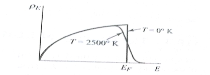
Fig. Energy distribution in metal at 0 & 2500 
Q3) Explain Hall effect in detail.
A3)
If a case (metal or semiconductor) carrying a current I is positioned in a slanting magnetic field B, be an electric field ε is induced in the path at right angles to both I and B. If I = qnAV, then the force exerted on a carrier due to the magnetic field will be qV *B. This observable fact, is recognized as the Hall Effect, is used to find out whether a semiconductor is n-type or p-type and to get the carrier concentration. Also at the same time measuring the conductivity σ, the mobility μ can be calculated.
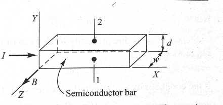
Fig Pertaining to the Hall Effect. The carriers are subjected to a magnetic force in the negative Y direction
In fig.4.3 I is in the positive X direction and B is in the positive Z direction, a force will be exerted in the negative Y direction on the current carriers. The current I may be due to holes moving from left to right or to free electrons traveling from right to left in the semiconductor specimen. Hence, autonomously of whether the carriers are holes or electrons, they will be forced downward toward side 1 in fig. 4.3. If the semiconductor is n-type material so that the current is carried by electrons, these electrons will gather on side I, and this exterior becomes negatively charged w.r.t. Side 2. Hence a potential called Hall voltage appears among surfaces 1 and 2.
If the polarity of  is positive at terminal 2, then as explained above, the carrier must be electrons. If on the additional hand, terminal I become charged positively w.r.t. Terminal 2, the semiconductor must be p-type. These outcomes have been proven experimentally, thus justifying the bipolar character of current in a semiconductor.
If I is the current in a p-type semiconductor, the carriers might be considered to be bound electrons jumping from right to left. Then side 1 would become negatively charged. However, experimentally, side 1 is set up to become positive w.r.t. Side 2 for a p-type specimen. This experiment confirms the quantum-mechanical fact that the hole acts like a free positive charge carrier.
Experimental Determination of Mobility
In the equilibrium state, the electric field intensity ε due to Hall effect must exert a force on the carrier which just balances the magnetic force, or
q ε = Bqv …………… (1)
Where q is the magnitude of the charge on the carrier, and v is the drift speed.
 ε where d is the distance between surfaces 1 and 2
J = ϱv= I/wd where J is the current density, ϱ is the charge density, and w is the width of the specimen in the direction in the direction of the magnetic field. Combining these relationships we find
 εd = Bvd =
  =
=  …….. (2)
If  B, I, and w are measured, the charge density ϱ can be determined from eq.(2). The Hall coefficient
  is determined by
 = 1/ϱ ….. (3)

 …….. (4)
If the conductivity is measured with the Hall coefficient, the mobility can be determined from
μ =  ……. (5)
Q4) What are Intrinsic & Extrinsic semiconductor?
A4)
Intrinsic Semiconductor
The pure elements like germanium (Ge) and silicon (Si) are called intrinsic semiconductor materials. In an intrinsic semiconductor material, the number of free electrons must equal the number of mobile holes. Their conductivity is intrinsic = K* e-E/KT ……. (1)
Extrinsic Semiconductor
These materials are doping materials in which impurities are added. In the extrinsic semiconductor two charge carriers, electrons and holes are present as a result of impurities built into the crystals. If B, Al, Ga, and ln are added, p-type semiconductor materials are obtained. If P and Sb are added, the N-type semiconductor materials are obtained.
Let us believe the boron to be added with germanium. The Boron (B) belongs to group III in the periodic table. The boron atom has three valence electrons and germanium has four valence electrons in its atom. One is remaining as a hole in the materials. This hole will be completed by some other electron from the neighborhood. The second hole may be completed by some other electron and so on. The conduction thus starts. The materials of this type are called p-type semiconductor materials.
Let Sb be added in germanium, Sb belongs to group V in the periodic table and it has 5 valence electrons, while that for germanium its four valence electrons. One electron is remaining. The remaining electron will revolve around the Sb atom in an orbit. The materials of this type are called N-type semiconductor materials.
Q5) Prepare electronic grade polycrystal in Siemens reactor.
A5)
Electronic grade silicon is a polycrystalline material and is extremely pure. So it is used for the preparation of single-crystal silicon.MGS is first grounded to powder form. Then it is treated with anhydrous hydrogen chloride (HCL) in a fluidized bed reactor to form trichlorosilane SiHCL3
 Si + 3HCL 300*C SiHCL3 + H2 …….. (1)
Trichlorosilane which is in liquid form at room temperature is fractionally distilled to acquire pure trichlorosilane and unnecessary impurities are detached. The purified SiHCL3 is compact by hydrogen in a reactor to form EGS by chemical Vapour deposition (CVD) process. The chemical reaction involved is
 2Si HCL3 + 2H2 2Si + 6 HCL …….. (2)
The machinery used to prepare EGS is shown in figure 4.4. A resistance heated bar of silicon. This results in the bar of EGS, which is polycrystalline in structure about 0.2 m in diameter and numerous meters in length. EGS is a slice from theses rods as single chunks.
EGS can also be produced from the pyrolysis of silane. In the CVD reactor of fig.4.4. Silane is used as an alternative of trichlorosilane and temperature is maintained around 900 *C. The follow-on equation is
 Si H4 + heat Si + 2H2 ...........(3)
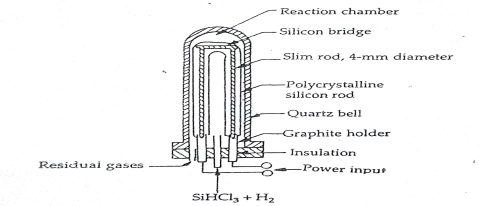
Fig. CVD Reactor for pyrolysis of silicon
Q6) Explain Czochrarloski Method.
A6)
This technique involves the solidification of atoms from a liquid phase at the interface. The growth speed is determined by the number of sites on the face of the crystal and the specifics of heat transfer at the interface. The apparatus used for CZ crystal growth is known as puller as shown in fig. 4.5. The puller is very bulky and at a time it can hold about 60 Kg of silicon. From which a crystal with 100 mm diameter and 3 m in length can be obtained. The puller has four main parts.
(i)Furnace
It includes a few silica crucibles, a graphite susceptor, a rotation mechanism, a heating element, and a power supply. The melt is containing crucible. So the crucible material can be chemically unreactive with the molten silicon. Since the electrical properties of silicon are highly sensitive to the presence of impurities that may be in small quantities. The melting point of crucible should be very high for thermal stability and hardness; also the crucible should be cost-effective and reusable.
Fused silica also reacts with silicon releasing the oxygen into the melt but the reaction is very slow and the purity of silica also affects the silicon purity. The alternative material for the crucible is silicon nitride which eliminates oxygen from crucible grown crystals. But again due to nitrogen erosion doping of the crystal with nitrogen takes place. The succeptor is used to support the silica crucible which also provides better thermal conditions. Graphite is used to make the susceptors as it has high-temperature properties.
The graphite used should be highly pure to prevent contamination of the crystal from impurities. The succeptor is placed on a pedestal whose shaft is connected to a motor that provides rotation. Radiofrequency heating or resistance heating is used to melt the charge. Radiofrequency heating is used for small melts and resistance heating is used for large melts. Finally, the graphite is connected to a dc power supply.
(ii)Crystal Pulling Mechanism
This mechanism should control the pull rate and crystal rotation so it should have minimum vibration and great precision. Seed crystal holder and pulling mechanism should maintain the proper orientation perpendicular to the melt surface. Lead screws are provided to withdraw and rotate crystal. The crystal leaves the furnace through a tube where ambient gas is directed along the surface of the crystal to reduce its temperature from the purge tube the crystal enters an upper chamber.
(iii)Ambient Control
This includes an inert gas source (of Argon) flow control and exhaust system. The gas source must meet the purity requirement. The inert gas environment is required because the hot graphite parts must be protected from oxygen. To prevent erosion and the gas around the process should not react with silicon.
(iv)Control System
The control system includes the control of process parameters like temperature, crystal diameter, pulled rate, rotation speed, etc. Program process steps are provided through microprocessor-based control. Infrared sensors are used to judge any change.
Working
The furnace is heated to melt silicon when polycrystalline silicon is positioned in the crucible. A properly leaning seed crystal is located over the crucible in the seed holder. The seed is deep into the melt. Some parts of seed melts and some touches the liquid surface. Freezing at the solid-liquid interface occurs and a single crystal is formed after the seed is slowly pulled up. The seed crystal is in the form of an ingot or silicon boule.
In the growth process, a known amount of dopant is added in the melt to obtain desired doping concentration in the grown crystal. Boron is added for p-type material and phosphorous for N-type material.
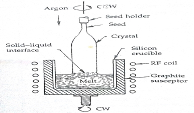
Fig CZ crystal growth apparatus
Q7) Explain Float Zone method of bulk single crystal ingot preparation
A7)
Float zone method is used when silicon with lower contamination is required. Czochalski technique grows silicon where the contamination level is high. The system showing the float zone process is shown in fig.4.6.
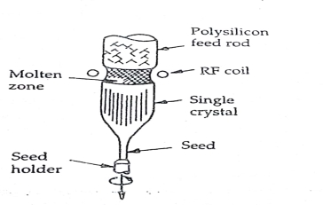
Fig. Float zone Process step
A purity polycrystalline rod with a seed crystal at the bottom is held in a vertical position. This system is then rotated. The rod is enclosed in a quartz envelope in which an inert atmosphere is maintained. A small zone of the crystal is kept molten by a radio frequency heater, which is moved from the seed up-ward so that the floating zone transverses the length of the rod. The molten silicon is retained by surface tension between the melting and growing solid silicon surface. As the floating zone moves upward, A single crystal silicon freezes at the zones retreating end and grows as an extension of the seed crystal. Since crucible is not used in this process, so no contamination from crucible reaches the melt. Float zone process is used when high power devices are made where high resistivity materials are required.
Q8) What is Mirror finished wafer preparation? How it is done?
A8)
Silicon, albeit brittle, is a hard material. The majority of appropriate material for shaping and cutting silicon is an industrial-grade diamond. Renovation of silicon ingots into refined wafers requires numerous machining, chemical, and polishing operations. After a grinding process to stick the diameter of the material one or more flats are stuck along the length of the ingot. The largest flat, called the "major" or "primary" flat, is generally comparable to particular crystal orientation. The flat is placed by x-ray diffraction techniques. The primary flat serves as a motorized locator in mechanized processing apparatus to place the wafer, and also serves to get used to the IC tool comparative to the crystal. Other minor flats are called "secondary" flats that afford to identify the orientation and conductivity kind of the wafer. Secondary flats thus offer a means to swiftly sort and recognize wafers should mixing happen. The flat locations for the four common types of silicon wafers are exhibited in Figure 3.8
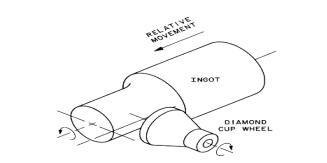
Fig..Schematic of the grinding process
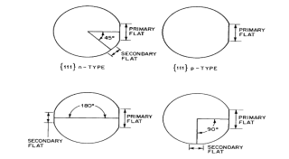
Fig. Identifying Flats on Silicon Wafer
The drawback of these flats is that the usable area on the wafer, i.e. the area on which microelectronic devices can be fabricated, is reduced. In support of a few 200 mm and 300 mm diameter wafers, only a minute notch is engraved from the wafer to allow lithographic grouping although no dopant type or crystal orientation information is conveyed. Just the once these operations have been completed, the ingot is ready to be sliced by diamond saw into wafers. Wafer parameters are determined by slicing: surface orientation (e.g., <111> or <100>); thickness (e.g., 0.5 –0.7 mm, depending on wafer diameter); taper, which is the wafer thickness variations from one end to another; and bend over, which is the exterior curvature of the wafer calculated from the middle of the wafer to its boundary. Later than slicing, the wafers experience a lapping procedure that is performed under pressure using a fusion of Al2O3and glycerine. Later chemical etching removes any residual damaged and impure regions. Traditionally, mixtures of hydrofluoric, nitric, and acetic acids have been employed, but alkaline etching, using potassium or sodium hydroxide, is also universal. Polishing is the concluding step. It intends to offer a smooth, specular surface on which device features can be photoengraved. Figure depicts the representation of a usual polishing machine and the method.
Q9) Explain Epitaxial film growth in detail.
A9)
Epitaxy is the combination of two Greek words: epi means “upon” and taxis means ordered. So a process used to grow a thin crystalline layer on a crystalline substrate is known as epitaxy. Tn this process the substrate acts as a seed crystal. Epitaxy is generally used to enhance the performance of bipolar transistors and other CMOS ICs. The collector resistance of the bipolar transistor can be reduced by epitaxial growth of a high resistivity layer on a low resistivity substrate. The substrate and the epitaxial layer opposite doping types to provide isolation and a heavily doped diffusion layer acts as a low resistance collector contact.
Types of the epitaxial process are discussed below:
(A) Chemical Vapour -Phase Epitaxy
Vapour phase epitaxy is the most important in the case of a silicon device and to some extent to gallium arsenide also. The vapor deposition of single-crystal silicon is performed in a reactor which consists of a quartz reaction chamber into which a susceptor is placed. The function of the susceptor is to provide physical support for the substrate wafers. This is a high-temperature process at which deposition takes place after several chemical reactions. The various kinds of susceptors and reactors used in the epitaxial process are discussed below. The commonly used susceptors are shown in fig.4.9.
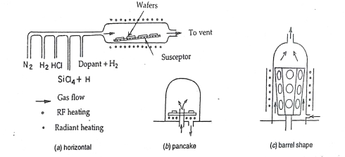
Fig. Susceptors for epitaxial growth
The susceptors are made from graphite blocks whether it is of horizontal, pancake, or barrel shape. They give mechanical support to the wafer and in induction heated reactors they also serve as the source of thermal energy for the reaction. Horizontal reactors offer lower-cost construction but controlling the deposition process throughout the length of the susceptor is a problem. Pancake reactors are capable of uniform deposition but they suffer from mechanical complexity. Barrel reactors are also used for a uniform deposition but are not suitable at temperatures more than 1200*C.
In most of the reactors the reaction tube is relatively cool during operation. Forced air cooling is done. Induction coils and the metal parts of the reactors are water-cooled.
The energy of the reaction is supplied by heating the susceptor inductively and the energy is transported to the wafer by conduction and radiation. Radiant heating provides more uniform heating than conductive heating.
Steps involved in the epitaxial process
A hydrogen carrier gas purges the reactor of air.
The reactor is heated to the required temperature.
An HCL etch takes place at a temperature between 1150 *C and 1200*C.
Then the temperature is reduced to growth temperature and the flushing of HCL takes place.
Silicon source and dopant flows are turned on and growth proceeds.
After growth, the dopant and silicon flows are removed and temperature reduces.
The hydrogen flow is replaced by a nitrogen flow to remove the wafers.
(B)Liquid Phase Epitaxy
When the growth of epitaxial layers on crystalline substrates by direct precipitation from the liquid phase takes place, it is known as the liquid phase epitaxy. This technique is mainly used for growing gallium arsenide and other III and V compounds. It is also very useful in growing very thin epitaxial layers as the growth rate is very small.
The boat configuration for the liquid phase epitaxy is shown in fig.3.10.In this arrangement, one or more wells are machined in a high purity graphite block which serves to hold the reactant solutions. A graphite slider holding the substrates is moved to locate them under the wells. This is placed in a furnace, in a neutral carrier gas(hydrogen) ambient. At a required temperature, the substrate is moved under the first well and the temperature of the furnace is lowered. The wafer is moved out from under the solution to stop the growth. For growing additional layers the substrate is moved successfully under other wells.
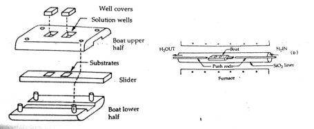
Fig. Boat Configuration for liquid phase epitaxy
One of the basic requirements of the liquid phase epitaxy is that the material to be grown dissolves in a solvent and the solution must melt at a temperature well below the melting point of the semiconductor substrate.
One method of liquid phase epitaxy for gallium arsenide is the equilibrium – cooling process. The solution is initially saturated with GaAs at a given temperature Ta with a composition Cm. The substrate also at Ta is inserted into the solution and the system temperature is slowly lowered. The solution is driven into a supersaturation state from which it proceeds toward equilibrium. This results in the growth of gallium arsenide.
A second method for Ga As growth is the step cooling process. In this gallium solution is saturated with gallium arsenide at a temperature Ta then the temperature is lowered to Tb and supersaturation of melt takes place. The substrate at temperature Tb is inserted into the melt. Growth occurs because of the supersaturation in the melt. Later on, the solution becomes depleted of gallium arsenide and the growth rate decreases.