UNIT-4
PHYSICS AND TECHNOLOGIES OF FET
Q1) Explain the construction of FET Structure?
A1)
- JFET is a current controlled device which allows current to pass from source to drain.
- The controlling voltage is applied between gate and source.
- The channel is an N-type or P-type semiconductor material.
All field-effect transistors are unipolar rather than bipolar devices. That is, the main current through them is comprised either of electrons through an N-type semiconductor or holes through a P-type semiconductor.
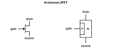 |
Figure1: N Channel JFET
In JFET, the controlled current passes from source to drain, or from drain to source. The controlling voltage is applied between the gate and source.
The current does not have to cross through a PN junction on its way between source and drain: the path (called a channel) is an uninterrupted block of semiconductor material.
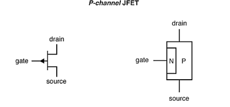
P-channel JFET
|
Figure 2: P Channel JFET
N-channel JFET are more commonly used than p-channel.
When no voltage is applied between the gate and source the channel is wide-open path for current to flow.
If voltage is applied between the gate and source the PN-junction is reverse biased and there is a flow between the source and the drain which becomes regulated.
Maximum gate to source voltage pinches off all current through source and drain forcing JFET into cut-off mode.
This behaviour is due to the depletion region of the PN junction expanding under the influence of a reverse-bias voltage, eventually occupying the entire width of the channel if the voltage is great enough.
When the gate-source PN junction is reverse biased there is zero current through the gate connection. Hence JFET is voltage- controlled device.
If the gate-source PN junction is forward-biased with small voltage the JFET channel will open allowing more current to flow through.
JFET: Construction & Operation
JFET is a three terminal semiconductor device in which current conduction is by one type of carrier that is electrons or holes.
The current conduction is controlled by means of an electric field between the gate and the conducting channel of the device.
The JFET has high input impedance and low noise level.
Construction Details:
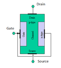
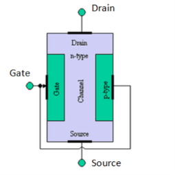
A JFET consists of a p-type or n-type silicon bar containing two p-n junctions at the sides as shown in figure.
|
p-type n-type
Figure 3: p-type and n-type Channel JFET
The bar forms the conducting channel for the charge carriers.
If the bar is of p-type, it is called p-channel JFET as shown in fig.a and if the bar is of n-type, it is called n-channel JFET as shown in fig.b.
The two p-n junctions forming diodes are connected internally and a common terminal called gate is taken out.
Other terminals are source and drain
Thus, a JFET has three terminals such as gate (G), source (S) and drain (D).
Fig. (i) shows the n-channel JFET polarities and fig. (ii) shows the p-channel JFET polarities.
|
|
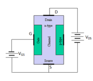 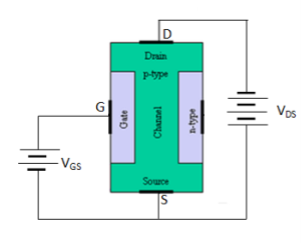 | |
Figure 4 (i): n-channel JFET polarities | Figure 4(ii): p-channel JFET polarities.
|
In each case, the voltage between the gate and source is such that the gate is reverse biased.
The source and the drain terminals are interchangeable.
The following points may be noted:
- The input circuit gate to source of a JFET is reverse biased. This means that the device has high input impedance.
- The drain is so biased with respect to source that drain current ID flows from the source to drain.
- In all JFETs, source current IS is equal to the drain current that is IS = ID.
Q2) Explain the construction of Principle and Working of JFET?
A2)
Principle and Working of JFET
The figure shows the circuit of n-channel JFET with normal polarities.
The two p-n junctions at the sides form two depletion layers.
The current conduction by charge carriers that is the electrons is through the channel between the two depletion layers and out of the drain.
The width and hence resistance of this channel can be controlled by changing the input voltage VGS.
The greater the reverse voltage VGS, the wider will be the depletion layer and narrower will be the conducting channel.
The narrower channel means greater resistance and hence source to drain current decreases.
Reverse will happen when VGS decreases.
Thus, JFET operates on the principle that width and hence resistance of the conducting channel can be varied by changing the reverse voltage VGS.
In other word, the magnitude of drain current ID can be changed by altering VGS.
The working of JFET can be explained as follows:
Case-i:
When a voltage VDS is applied between drain and source terminals and voltage on the gate is zero as shown in fig.(i), the two p-n junctions at the sides of the bar establish depletion layers.
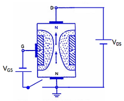 |
Figure 5 (i): working of JFET
The electrons will flow from source to drain through a channel between the depletion layers.
The size of the depletion layers determines the width of the channel and hence current conduction through the bar.
Case-ii:
When a reverse voltage VGS is applied between gate and source terminals, as shown in fig.(ii), the width of depletion layer is increased.
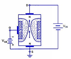 |
Figure 5 (ii): working of JFET
This reduces the width of conducting channel, thereby increasing the resistance of n-type bar.
Consequently, the current from source to drain is decreased.
On the other hand, when the reverse bias on the gate is decreased, the width of the depletion layer also decreases.
This increases the width of the conducting channel and hence source to drain current.
A p-channel JFET operates in the same manner as an n-channel JFET except that channel current carriers will be the holes instead of electrons and polarities of VGS and VDS are reversed.
Schematic Symbol of JFET
Fig.shows the schematic symbol of JFET.
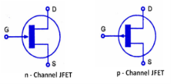 |
Figure 6: Symbol of JFET
Advantages of JFET
A JFET is a voltage controlled, constant current device in which variation in input voltage control the output current.
Some of the advantages of JFET are:
- It has a very high input impedance. This permits high degree of isolation between the input and output circuits.
- The operation of a JFET depends upon the bulk material current carriers that do not cross junctions. Therefore, the inherent noise of tubes and those of transistors are not present in a JFET.
- A JFET has a negative temperature co-efficient of resistance. This avoids the risk of thermal runaway.
- A JFET has a very high power gain. This eliminates the necessity of using driver stages.
- A JFET has a smaller size, longer life and high efficiency
Q3) Explain JFET Drain and transfer Characteristics?
A3)
Drain Characteristics
In the absence of external bias: When there is no voltage between gate and source terminal, thus, the drain current will flow from drain terminal to source terminal.
In JFET the majority charge carriers flow from source to drain and because of which the current flows from drain to source.
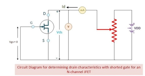 |
Figure 7: Drain Characteristics of N channel JFET
It clearly implies that the channel width is more as the width of depletion layer will not vary initially because there is no external reverse biasing. This allows a large magnitude of current to flow through the channel.
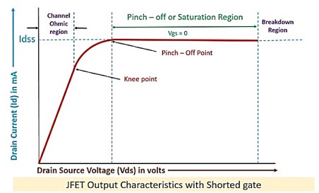 |
Figure 8: JFET output characteristics
In this case, the N-type channel will simply behave as resistance region. The flow of current from drain to source will create the voltage drop between gate and source. This will eventually result in reverse biasing of the gate-source terminal. The reverse biasing will be more towards drain region that source region.
Terminologies involved in JFET characteristics
- Knee Point: There exists a point in the characteristics curve where the variation of drain current with drain-source voltage appears to be linear. But after this point, the linearity changes into a curve.
- Channel Ohmic Region: The region to the left of the knee point in the characteristics curve is the channel ohmic region.
- Pinch-off point: The point in the curve above which the drain current does not increases further no matter how much we are increasing the drain to source voltage, this point is termed as the pinch-off point.
- Pinch-off Voltage: The voltage at the pinch-off point is termed as pinch-off voltage because at this voltage the current is completely turned to be constant.
- Drain-Source Saturation Current: The drain to source saturation current is the current which becomes constant or completely enters a saturation state.
The region after the pinch-off point in the curve is termed as saturation region. When the JFET is allowed to work as an amplification device, the JFET utilizes this region for operation.
2. With external bias: When the external bias is applied to the gate-source terminal, the gate-source terminal becomes reversed bias externally. The pinch-off point is early as compared to the circuit which is not biased.
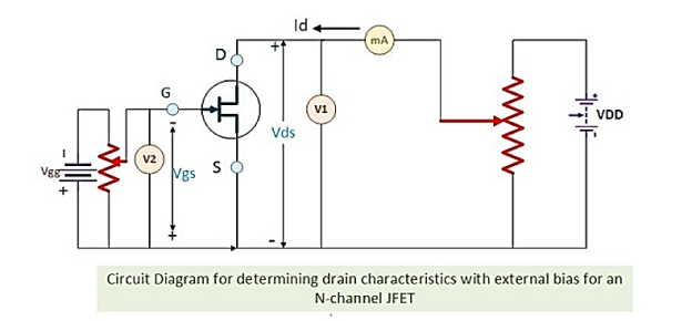 |
Figure 9: Drain Characteristics of N channel JFET with external bias
The different values of voltage give different values of current. Here the drain characteristics with respect to the variation in drain-source voltage is observed by keeping the gate-source voltage constant.
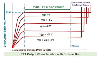 |
Figure 10: JFET output characteristics with external bias
JFET TRANSFER CHARACTERISTICS
Transfer Characteristics
The transfer characteristics can be determined by observing different values of drain current with variation in gate-source voltage provided that the drain-source voltage should be constant. The transfer characteristics are just opposite to drain characteristics.
In transfer characteristics we are keeping the value of drain-source voltage constant.
The characteristic curve of transfer characteristics of JFET is shown below. It is observed that the value of drain current varies inversely with respect to gate-source voltage when the drain-source voltage is constant.
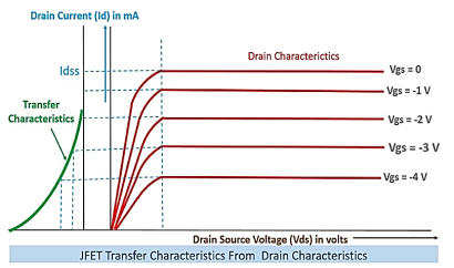 |
Figure 11: JFET Transfer Characteristics from drain Characteristics
Q4) Explain energy band diagram for MOS Capacitor?
A4)
MOS stands for metal–oxide–semiconductor. The MOS capacitor is just an oxide placed between a semiconductor and a metal gate. The semiconductor and the metal gate are the two plates of the capacitor. The oxide functions as the dielectric. The area of the metal gate defines the area of the capacitor.
An MOS capacitor is made of a semiconductor body or substrate, an insulator film and a metal electrode called a gate. The oxide film can be as thin as 1.5 nm.
A second metal layer forms an Ohmic contact to the back of the semiconductor and is called the bulk contact. The structure shown has a p-type substrate. We will refer to this as an n-type MOS or nMOS capacitor since the inversion layer contains electrons.
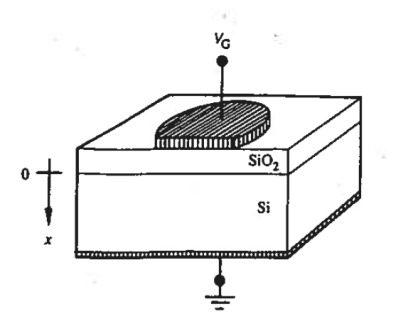 |
Figure 12: MOS capacitor
The ideal MOS structure should have the following properties:
- Semiconductor should be uniformly doped
- The metallic gate is made sufficiently thick for the a.c. And d.c. biasing conditions
- The oxide layer should be insulator so that no zero current can flow through it under all static biasing conditions.
- There are no charge canters located in the oxide or at the oxide—semiconductor interface
- The semiconductor is sufficiently thick so that, regardless of the applied gate potential, a field-free region is encountered before reaching the back contact
- An ohmic contact has been established between the semiconductor and the metal on the back side of the device.
- The MOS-C is a one-dimensional structure with all variables taken to be a function only of the x-coordinate
ENERGY BAND DIAGRAM
To study the internal status of the MOS structure under static biasing conditions, we will study the energy diagram of it. From energy band diagram we will come to know more details about the internal structure of MOS.
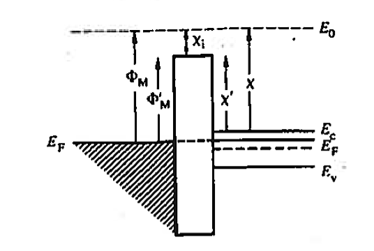 |
Figure 13: Energy band diagram
Let us consider the ideal MOS structure under zero biasing conditions. Some important points to keep in mind to study the band diagram.
- E0 is the minimum energy an electron possesses to completely free itself from the material.
- The energy difference between the vacuum level and the Fermi energy in a metal is known as the metal work-function ΦM.
- In the semiconductor the height of the surface energy barrier is specified in terms of the electron affinity χ.
- The energy difference between the vacuum level and the conduction band edge at the surface is written as E0- EF = χ because the quantity is not a constant in semiconductors, but varies as a function of doping and band bending near the surface.
- (E,-EF)FB = the energy difference between E and EF in the flat band or field-free portion of the semiconductor.
The conceptual formation of the MOS zero-bias band diagram from the individual components is a two-step process.
Initially the metal and semiconductor are brought together until they are a distance x0 apart and both the components of the system must be in equilibrium. The system is in equilibrium simply implies that Fermi levels of metal and semiconductor must have the same energy. Moreover, the vacuum levels of the M and S components must also be in alignment because ΦM = ΦS. This implies that there are no charges or electric fields anywhere in the metal-gap-semiconductor system.
The insulator of thickness x0 is inserted into the empty space between the metal and semiconductor components. Given the zero electric field in the x0 gap, the only effect of inserting the insulator is to slightly lower the barrier between the M and S components. Thus the equilibrium energy band diagram for the ideal MOS structure is shown in figure 13
Q5) Discuss modes of operation for MOS Capacitor?
A5)
MODES OF OPERATION
The capacitance value of a capacitor doesn't change with values of voltage applied across its terminals. However, this is not the case with MOS capacitor. We find that the capacitance of MOS capacitor changes its value with the variation in Gate voltage. This is because application of gate voltage results in band bending in substrate and hence variation in charge concentration at interface.
Depending upon the value of gate voltage applied, the MOS capacitor works in three modes:
Accumulation: In this mode, VG <0, there is accumulation of holes at the interface. Accumulation occurs typically for negative voltages where the negative charge on the gate attracts holes from the substrate to the oxide-semiconductor interface. With no voltage applied, a p-type semiconductor has holes, or majority carriers, in the valence band. When a negative voltage is applied between the metal gate and the semiconductor, more holes will appear in the valence band at the oxide-semiconductor interface. This is because the negative charge of the metal causes an equal net positive charge to accumulate at the interface between the semiconductor and the oxide. This state of the p-type semiconductor is called accumulation.
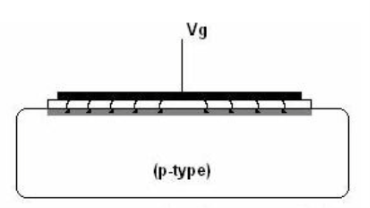 |
Figure 14: Accumulation
Depletion: Depletion occurs for positive voltages. As we move from negative to positive gate voltages the holes at the interface are repelled and pushed back into the bulk leaving a depleted layer. Therefore, the semiconductor is depleted of mobile carriers at the interface and a negative charge, due to the ionized acceptor ions, is left in the space charge region. The voltage separating the accumulation and depletion regime is referred to as the flatland voltage, VFB.
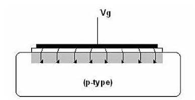 |
Figure 15: Depletion
Strong Inversion: When VG crosses threshold voltage, the increase in depletion region width stops and charge on layer is countered by mobile electrons at interface. This is called inversion because the mobile charges are opposite to the type of charges found in substrate. In this case the inversion layer is formed by the electrons. Field lines hence terminate on this layer thereby reducing the effective dielectric thickness as shown in Figure.
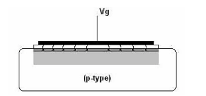 |
Figure 16: Strong Inversion
Q6) Discuss gate-voltage relationship for MOS Capacitor?
A6)
GATE-VOLTAGE RELATIONSHIP
VG in the ideal structure is dropped partly across the oxide and partly across the semiconductor and can be written as
 ………..(1)
Because ϕ = 0 in the semiconductor bulk, however, the voltage drop across the semiconductor is simply
 ………..(2)
The task of developing a relationship between VG and ϕs is therefore reduced to the problem of expressing  ox in terms of ϕs.
For an ideal insulator with no carriers or charge centers
 ………..(3)
And
 ………..(4)
Therefore
 ………..(5)
Where x0 is the oxide thickness. The next step is to relate to, ox to the electric field in the semiconductor. The well-known boundary condition on the fields normal to an interface between two dissimilar materials requires
 ………..(6)
Where D=Ɛ is the dielectric displacement and Qo-s is the charge/unit area located at the interface. Since Qo-s = 0 in the idealized structure, so we have
 ………..(7)
 ………..(8)
And
 ………..(9)
Ks is the semiconductor dielectric constant; Ko, the oxide dielectric constant; and S the electric field in the semiconductor at the oxide -semiconductor interface.
Finally, substituting equation (2) and (9) in (1), we have
 ………..(10)
Where S is given by the following relation
 ………..(11)
So gate voltage is given by
 ………..(12)
Q7) Discuss capacitance-voltage characteristics MOS Capacitor?
A7)
CAPACITANCE-VOLTAGE CHARACTERISTICS
The capacitance–voltage (C–V) measurement is a powerful and commonly used method of determining the gate oxide thickness, substrate doping concentration, threshold voltage, and flat-band voltage.
With d.c. Current flow blocked by the oxide, the major observable exhibited by MOS-Cs is capacitance. The varies as a function of the applied gate voltage.
To explain the observed farm of the C—V characteristics, let us consider how the charge inside an n-type MOS-C responds to the applied ac. Signal as the d.c. Bias is systematically changed from accumulation, through depletion, to inversion.
Accumulation: We know that accumulation with d.c. State is characterized by the pileup of majority carriers right at the oxide-semiconductor interface and state of the system can be changed very rapidly. Only majority carriers are involving in this process.
The device can follow the applied a.c. Signal quasistatically. Since the a.c. Signal merely adds or subtracts a charge close to the edges of an insulator, the small a.c. signal adding or subtracting a small  Q on the two sides of the oxide as shown in Figure 17(a). Thus the charge configuration of charges inside MOS-C is similar ordinary parallel-plate capacitor.
For both low or high frequencies, we have
 ………..(1)
Where Ao is the area of the MOS-C gate.
Depletion: Under depletion biasing the d.c. Stale of an n-type MOS structure is characterized by a -Q charge on the gate and a +Q depletion layer charge in the semiconductor. The depletion layer charge is related the removal of majority
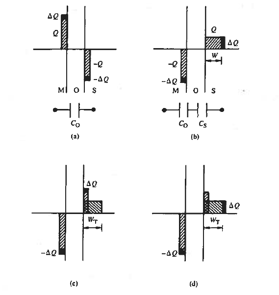 |
Figure 17: a.c. Charge fluctuation inside an n-type MOS-capacitor under d.c. Biasing (a) accumulation (b) depletion, (c) inversion (ω ), (d) inversion (ω
 )
)
Carriers from an effective width W adjacent to the oxide-semiconductor interface. State of the system can be changed very rapidly. Only majority carriers are involve in this process.
When the a c. Signal applied, it increases negative charge on the MOS-C gate and the width of depletion layer inside the semiconductor also increases then it starts fluctuating about its d.c. value.
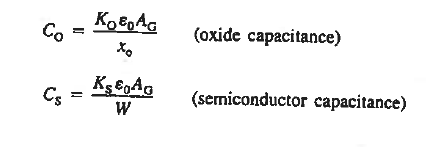
Now if the stationary d.c. Charge is conceptually eliminated. All that remains is a small fluctuating charge on the two sides of a double-layer insulator. For all frequencies this situation is clearly similar to two parallel plate capacitors (Co and Cs) in series, where
|
It is clear from equation (3) because W increases with increased depletion biasing, C(depl) correspondingly decreases as the d.c. bias is changed from flat band to the onset of inversion.
Inversion: Once inversion is achieved an appreciable number of minority carriers pile up near the oxide-semiconductor interface in response to the applied d.c. Bias. Also, the d.c. width of the depletion layer tends to maximize at WT. But the response to ac signal is not as quick.
The inversion layer charges fluctuate in response to the a.c. Signal. The observed charge fluctuation depends on the frequency of the at signal used in the capacitance measurement.
For low frequency(ω ),
),

For high frequency (ω )
)

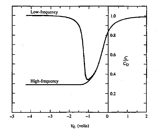
We expect the MOS-C capacitance to be approximately constant at Co under accumulation biases, to decrease as the d.c. Bias progresses through depletion, and to be approximately constant again under inversion biases at a value equal to Co if ω w 0 or C(depl)min, if ω
 .
.
C-V characteristics shown in figure below
|
Figure 18: C-V Characteristics
Q8) Discuss metal-semiconductor work function difference for non-ideal MOS?
A8)
METAL--SEMICONDUCTOR WORKFUNCTION DIFFERENCE
We already studied that energy band diagrams provide complete information of the structure. Let us take a look at the energy band diagrams for the isolated components of an Al—Si02—(p-type) Si system.
We found out that in a real device the energy difference between the Fermi energy and the vacuum level is unlikely to be the same in the isolated metal and semiconductor components of the system; that is, in contrast to the ideal structure.
ΦM  ΦS = χ+(EC-EF)FB……………(1)
To study the real systems, we need to modify the ideal theory.
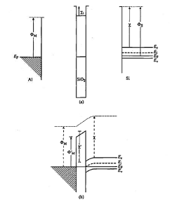
Let us begin with constructing the equilibrium (VG = 0) energy band diagram for the system whose independent components shown in of Figure 27(a).
We start it by joining the outer ends of the metal and semiconductor through a wire. The two materials are then brought together in a vacuum until they are a distance xo apart. The connecting wire helps the transfer of charge between the metal and semiconductor and helps maintain the system in an equilibrium state where the respective Fermi levels "line up" as the materials are brought together.
With the metal EF and semiconductor EF at the same energy, and ΦM  χ+(EC-EF)FB the vacuum levels in the two materials must be at different energies. Thus an electric field develops between the components.
Moreover, band bending occurs inside the semiconductor. VAC and the semiconductor band balding increase as the components are brought closer and closer together. The metal and semiconductor are at distance x0, now if we insert insulator between them it lowers the effective surface barriers and reduces the electric field in the x0, region (K0 > I).
Also ΦM  ΦM - χi
  M and χ
  χ - χi = χ’
|
Figure 27: (a) To scale energy band diagram. For the isolated components Al-Si02-S, area (b) Equilibrium energy band diagram typical of real MOS Structure.
So we concluded
- The work-function difference modifies the relationship between the Semiconductor Surface Potential and the applied gate voltage.
- By setting VG=0 does not give rise to flat band conditions inside the semiconductor.
- Like in a pn junction or MS diode, time is a built in potential.
Built-in potential Vbi can be determined by equating the energies from the Fermi level to the top of the band diagram as viewed from the two side of the insulator. We get
 Taking metal as zero potential reference point we get built in potential  Where 
|
Perhaps the result should have been intuitively obvious: The built-in potential inside ΦM  ΦS but otherwise ideal. MOS structure is just the metal-semiconductor work function difference expressed in volts.
ΦMS  is minor non ideality as it leads to shift voltage to smaller extent which is easily predictable and is not capable of creating instabilities in the device.
Q9) Discuss oxide charges for non-ideal MOS?
A9)
OXIDE CHARGES
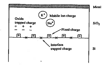
Oxide charge affects the system more significantly. It leads to shift voltage to larger extent and cause instabilities.
|
Figure 28: Oxide charge
The nature and position of the oxide charges are summarized in Figure. A number of distinct charge canters have been identified actually within the oxide or at the Si-Si02 interface.
Effect of oxide charges: Let us postulate the existence of a charge distribution, ρox(x) that varies in an arbitrary manner across the width of the oxide layer. The origin of the x coordinate has been relocated at the metal—oxide interface.
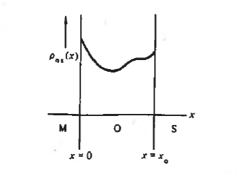
|
Figure 29: Arbitrary distribution of oxide charges
Recall the following expression
   The double integral in Eq. (3) can be reduced to a single integral employing integration by parts. Moreover ox (x0) = KsS/ Ko if a plane of charge is excluded from oxide semiconductor interface.  VG = ΦS +   However, for an ideal device  Thus  |
Q10) Explain the Threshold considerations and Threshold adjustment for non-ideal MOS?
A10)
THRESHOLD ADJUSTMENT AND CONSIDERATIONS
Threshold considerations
The VT point on the C V curve, corresponding to the threshold voltage of a MOSFET, is of course directly affected by any  VG displacement.
Figure 30(a) graphically illustrates the general effect of changes in the threshold voltage on the MOSFET ID—VD characteristics. A hypothetical p-channel MOSFET with an ideal device V’T = -1V was assumed in constructing the figure. The  VG leading to the perturbed characteristics in Figure 30(a) is caused by ΦMS, the fixed charge, and/or alkali ions in the oxide.
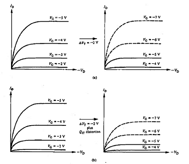 |
Figure 30: General effect of nonidealities on the MOSFET (a) shift in the threshold caused by ΦMS, the fixed charge, and/or alkali ions in the oxide. (b) Degrading effect of interfacial traps.
Note that, analogous to the parallel translation of the MOS-C C—V characteristics, the form of the perturbed MOSFET characteristics is unchanged, but larger VG values are needed to achieve comparable ID current levels. If present in large densities, the interfacial traps can additionally decrease the change in current resulting from a stepped increase in gate voltage. This effect, equivalent to a reduction in the gm, of the transistor, is pictured in Figure 30(b).
While it is true that both the mobile ion and interfacial trap problems were minimized early in MOSET development, the remaining nonidealities, primarily through their effect on VT, have had a very large impact on fabrication technology, device design, and modes of operation.
Threshold adjustment
Several physical factors affect the threshold voltage and can therefore be used to vary the VT actually exhibited by a given MOSFET.
- By varying the oxide thickness, we can adjustment VT.
- The substrate doping can also be varied to increase or decrease the threshold voltage.
However, the gate-oxide thickness and substrate doping are predetermined in large part by other design restraints.
Other factors that play a significant role in determining VT are; The substrate surface orientation and the material used in forming the MOS gate. The QF in MOS devices constructed on (100) surfaces is approximately three times smaller than the QF in devices constructed on (11 l) surfaces. The use of (100) substrates therefore reduces the  VG associated with the fixed oxide charge. The use of a polysilicon instead of Al gate can change the ΦMS
For a number of reasons, it is very desirable to have a flexible threshold adjustment process where VT can be controlled essentially at will. In modern device processing this is accomplished through the use of ion implantation.
Ion Implantation
- To adjust the threshold voltage, a relatively small, precisely controlled number of either boron or phosphorus ions are implanted into the near-surface region of the semiconductor.
- When the MOS structure is depletion or inversion biased, the implanted dopant adds to the exposed dopant-ion charge near the oxide semiconductor interface and thereby translates the VT exhibited by the structure.
- The implantation of boron causes a positive shift in the threshold voltage; phosphorus implantation causes a negative voltage shift.
If N1 is the number of implanted ions/cm2 and Qt = q N1 is the implant-related donor (+) or acceptor (-) charge/cm2 at the oxide-semiconductor interface, then, by analogy with the fixed charge analysis

Assuming, for example, an N1 = 5 X 10¹¹boron ions/cm2 and x0 = 0.1 μm, computes threshold adjustment of ± 2.32 V.
Q11) An amplifier has a signal i/p Vtg. Vi of 0.25v and draws 1mA from the source. The amɤ delivers & v to a load at 10 mA. Determine the current Vtg and power gains. Also find the i/p resistance of this ampɤ what must be the open ckt. Vtg of the source Vs to provide an ampɤ i/p VtgVi of 0.25 v when the internal resistance of the source is 50 Ω?
A11)
Given Vi = 0.25v, Ii = 1 Ma, Vo = 8 v, Io = 10 mA, Rs = 50 Ω.
Solution:
Vtg gain Av = 
Current gain =
= 
Power gain AP = Av  = 32
= 32 
Input resistance Ri =  = 250
= 250
Open circuit Vtg of Vs
Vi = 
Vs = 
Vs = 
Vs = 0.3v
Q12) Explain type and operation and V-I Characteristics ssof MOSFET?
A12)
MOSFET is another type of field effect transistor. The MOSFET has become one of the most important devices used in design and construction computers
MOSFET [metal oxide semiconductor field effect transistor]
Type of MOSFET
- Depletion type MOSFET
- Enhancement type MOSFET
- Power MOSFET
Enhancement type MOSFET: classified in to two type n. Channel or p. Channel E MOSFET
A) N-channel E MOSFET
B) P-channel E MOSFET
N-channel E MOSFET
|
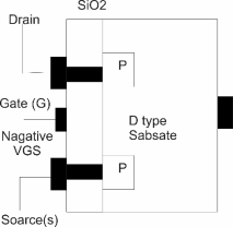
Figure 19: N-channel E MOSFET
- A slab of P-type semiconductor is used as substrate. The substrate is sometimes connected to the source otherwise it is brought out as the fourth terminal.
- The drain and source terminal are connected to the n-type doped regions through the metallic contacts.
- The insulating sio2 layer is still present which isolates gate terminal from the substrate.
Effect of the insulting sio2 layer:
Due to the presence of the sio2 layer between gate terminal and n-type channel the i/p impedance of MOSFET is very high this is a desirable fracture of a MOSFET. Due to high i/p impedance the gate current IG= 0 for the d.c operating conditions.
Operation: the operation can be explained with two different operating
- Operation with VGS = 0
- Operation when VGS is +ve
1) Operating with VGS = 0 Volt
If VGS = 0 and a positive voltage is applied between its drain and source, then due to the absence of the n-type channel a zero drain current will result.
2) Operation when Vgs Positive:
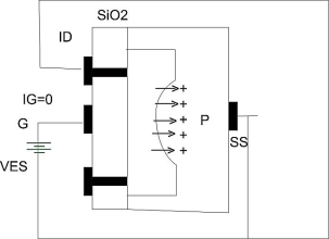
The positive potential at the gate terminal will repel the holes present in the p-type substrate.
|
Figure 20: Operation on N-channel E MOSFET
Formation of induced channel in n-channel enhancement MOSFET
This creates a depletion region near the sio2 insulating layer. But the minority carriers ie the electrons in the p-type substrate will be attracted towards the gate terminal and gather near the surface of sio2 as shown above
As we increase the positive VGS the number of e- gathering near the sio2 layer increases to such an extent that it creates an induced n-channel which connects the n-type doped regions.
The drain current then starts flowing through this induced channel. The value of VGS at which this conduction begins is called as the threshold Vtg. & is indicated.
V-I Characteristics
Characteristics of n-channel enhancement type MOSFET:
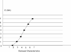 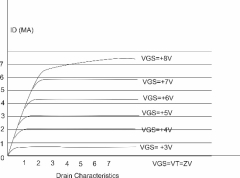
|
Transfer characteristics drain characteristics
Figure 21: Characteristics of n-channel enhancement type MOSFET
P-channel enhancement type MOSFETS:
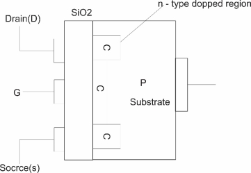 |
Figure 22: P-channel enhancement type MOSFETS
The construction of p-channel EMOSFET is exactly opposite to that of a n-channel EMOSFET
Characteristics:
Drain Characteristics of transfer Characteristics of p-channel E MOSFET
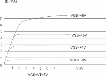 |
Figure 23: Characteristics of p-channel enhancement type MOSFET
Regions of Operation, MOSFET as Switch & Amplifier
Operation: the operation can be explained with two different operating
Operation with VGS = 0
Operation when VGS is +ve
Operating with VGS = 0 Volt
If VGS = 0 and a positive voltage is applied between its drain and source then due to the absence of the n-type channel a zero drain current will result.
Operation when Vgs Positive:
The positive potential at the gate terminal will repel the holes present in the p-type substrate.
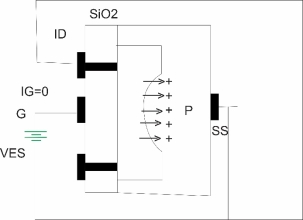 |
Figure 24: Formation of induced channel in n-channel enhancement MOSFET
Formation of induced channel in n-channel enhancement MOSFET
- This creates a depletion region near the sio2 insulating layer. But the minority carriers i.e. the electrons in the p-type substrate will be attracted towards the gate terminal and gather near the surface of sio2 as shown above
- As we increase the positive VGS the number of e- gathering near the sio2 layer increases to such an extent that it creates an induced n-channel which connects the n-type doped regions.
- The drain current then starts flowing through this induced channel. The value of VGS at which this conduction begins is called as the threshold Vtg. & is indicated
Effect of increase in the drain to source Vtg. :
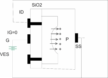 |
Figure 25: Effect of increase in the drain to source Vtg :
Effect of changes in VDS at fixed VGS on the channel width
- The positive gate to source voltage VDS is kept constant and the drain to source voltage VGS is increased gradually.
- Due to this the gate terminal becomes less and less positive with respect to the drain so less number of electron are attracted towards gate terminal & the induced channel becomes narrow.
- Eventually the channel width will be reduced to a point of pinch off and the saturation condition will be established which is same as that in a JFET
- That means any further increase in VDS at the fixed value of VGS will not affect the saturation level of ID unless breakdown condition are encountered.
- Symbols:
1) N-channel EMOSFET2) P-channel EMOSFEJ
BJT is a bipolar device [minority & majority carriers both contributes to the current flow]
E MOSFET is a unipolar device ie current flows only due to the majority carriers
BJT thermal runaway can damage BJT thermal runway does not take place.
BJT low i/p impedance, E MOSFET High i/p impedance
- Voltage ampɤ :
- Current and vtg gain
Current gain AI is defined as the ratio of o/p current

Vtg gain is given by
Av = Vo/Vi

In this expression if Ro is very small as compared to RL then Av A
A
Thus we can say that the overall gain of the ampɤie Av will approach its open circuit value A if Ro << RL