Unit - 3
Frequency Compensation & Nonlinearity
Q1) In a summing amplifier, if R = 1kΩ, Va = +3V, Vb = +8V, Vc = +9V, Vd = +5V and supply voltage is ±15V. Find the output voltage Vo.
A1) Vo = Sum of all input voltages applied at both the terminals
Vo = Va + Vb + Vc +Vd
Vo = -3 -8 +9 +5
Vo = +3V
Q2) Find the output voltage for the given circuit diagram if Rf = 5kΩ.
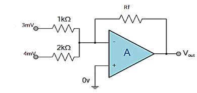
A2)
We know,
Gain (Av) = =
= 
Hence,
Av1 = 
Av2 = 
Now, Output voltage Vo = Sum of the two amplified input signals
Vo = Av1 x V1 + Av2 x V2
Vo =(-5 x 3) + ( -2.5x 4) mV
Vo = -25mV
As the above output voltage is negative hence it is an inverting amplifier.
Q3) The integrator circuit as shown in the figure has R = 500K Ω and C=1µF. Find and plot the output voltage for the inputs as shown in the figure.
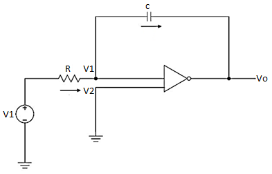
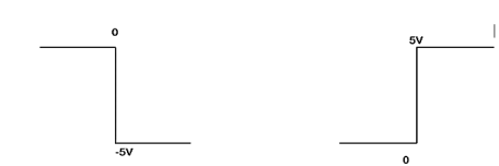
a) b)
c)vi= 2 sin 4tV d) vi= 4tV
A3)
We know that
v0 = - 1/RC  + v0(0)
Here R= 500K Ω and C = 1µF
1/RC = 1/ 500 x 1000 x 1 x 10-6
= 1/RC = 2
= -2  ; vi =- 5V
= -2 
= 10t V
Which means it is a ramp voltage with positive slope.
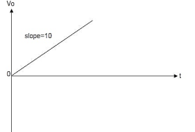
When vi=5V
-2  ; vi = 5V
= -2 
= -10t V
Which means it is a ramp voltage with negative slope.
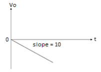
When vi= 2 sin4t V
Vo = -2 
= -4 [-cos 4t] /4 = cos 4t
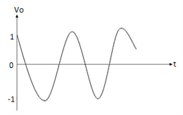
When vi=4t V
Vo = 
= -8 [t2/2] = - 4V
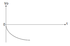
Q4) The VREF = VCC = 5 volts and the three resistors will be the same 10k ohms. So calculate the voltage at the A node. Assume Vout =0V and 5V.
A4)
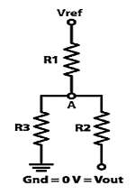
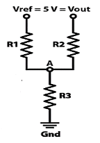
Vout = 0V

Va = 166V
Vout = 5V

Va = 333V
Q5) A 200mV peak to peak sine waveform voltage is applied to Op-amp inverting amplifier with Rf/R1 = 10.
A5) Peak to peak input voltage
2Vm = 200 mV
Vm = 100 mV
Vi= Vm sin wt = 100 sin wt mV
Vo = -Rf/R1 x vi = -10 x 100 sinwt mV
= -1000 sin wt mV
Q6) Design a non-inverting amplifier using Op-amp with a closed loop voltage gain of 10.
A6)
Af = 1 + Rf/R1 =10
Rf/R1 = 9
Rf = 9 R1
If R1 = 1K
Rf = 9K Ω
Q7) In an op-amp inverting amplifier R1 = 1K Ω and Rf = 100KΩ. The DC supply voltage of the op-amp is ± 15V. Calculate the output voltage if input voltage is 1V.
A7)
R1 = 1KΩ Rf = 100KΩ
V+ = 15V and V-=-15V. Vi = 1V
Af = -Rf/R1 = -100K/1K = -100
Af = vo/vi
Vo = Af vi
= -100 x 1V = -100V
The output voltage cannot exceed the DC power supply voltage. Since vo is negative and large it is limited to V-
Vo ≈ V- = -15V
Q8) Compare inverting, non-inverting and differential amplifier?
A8)
Basis of Comparison | Inverting Amplifier | Non-Inverting Amplifier |
Basic | It provides an amplified signal which is out of phase with the applied input. | It is designed to provide an amplified signal which is in phase with the signal present at the input.
|
Phase difference between input and output |  |  |
Input | Applied at negative input terminal | Provided at positive input terminal |
Achieved output | Inverted in nature | Non-Inverted in nature |
Expressed as | Negativity polarity | Positive polarity |
Gain of Amplifier | Ratio of resistances | Summation of 1 with the ratio of resistances. |
Ground connection | The positive input terminal is grounded. | The negative input terminal is grounded. |
Gain Polarity | Negative | Positive |
Q9) Two direct-coupled CE amplifiers are placed in series to achieve the desired voltage gain. Design a level shifter to be placed in between the two CE amplifiers to provide a dc voltage sufficiently low to prevent the second CE amplifier from saturating. Do this by providing a 1 V bias to the second stage. The collector voltage, VC, of the first amplifier is 4 V, and the RC of that amplifier is 1 kΩ. Design the level shifter to have an IC of 1 mA using a 10V power supply. Use a current source having β(s) = 100, VBE(s) = 0.7 V, and VON = 0.7 V.
A9) We need to find the values of RE, R1, R2, and R’E. Since the first amplifier has a VC of 4 V, the value of VBB is 4 V, whereas the RB of that formula is 1 kΩ. Note this is using the Thevenin equivalent circuit of the previous amplifier.

Setting the current-source transistor operating point in the middle of the dc load line, we have

And


The voltage across R’E is 5.5 V. Then


We now know the voltages across R1 and R2 and the parallel resistance. This yields two equations, where we assume that the base current in the lower transistor of Figure 9.7(b) is negligible.


And


The design is therefore complete.
Q10) Explain the types of external frequency compensation?
A10) Dominant pole Compensation
This technique uses a simple RC network connected across the output of the operational amplifier circuit. A sample dominant pole compensation circuit is shown below.
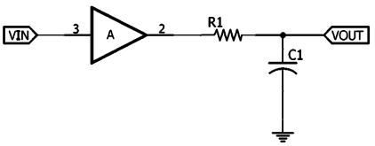
Fig: Dominant Pole Compensation
This works great to overcome the instability issue. The RC network creates a pole at unity or 0dB gain that dominates or cancels out other high-frequency poles effect. The transfer function of the dominant pole configuration is –

Where, A(s)is the uncompensated transfer function, A is the open-loop gain, ώ1,ώ2, and ώ3 are the frequencies where the gain roll-off at -20dB, -40dB, -60dB respectively. The Bode plot below shows what happens if the dominant pole compensation technique is added across the op-amp output, where fd is the dominant pole frequency.
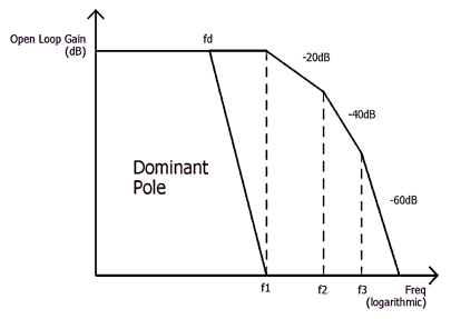
Fig: Dominant Pole Frequency
Pole Zero compensation:
Consider an op-amp with 3 break frequencies. Its loop gain be A.

Here the transfer function A is modified by adding a pole and zero with the help of compensating network. The zero added is at HF while the pole is at LF. Such a network is shown in figure
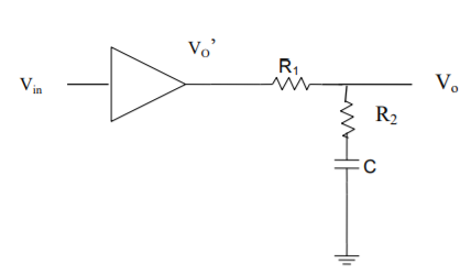
Fig: Pole Zero Compensation
Let A1 be the transfer function of the compensating network = Vo / Vo’
Let Z1=R1 & Z2 = R2-jXC2
By Voltage Divider rule,

On simplification,

On Simplification

Now let


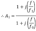
The values of Resistors and Capacitors are so selected that the break frequency for zero matches with the first corner frequency f1 of the uncompensated system while the pole of the compensating network at fo passes through 0 dB at the second corner frequency f2 of the uncompensated system. The loop gain becomes A’ = AA1.
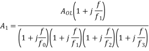
Where 0<f0<f1<f2. The, first corner frequency is now fo, and the gain starts rolling off at -20 dB / decade at fo. At f = f1, there is pole zero cancellation and rolling rate continues as -20 dB / decade. The values of Resistors and Capacitors are so selected that plot passes through 0 dB at f2. The response is shown in figure
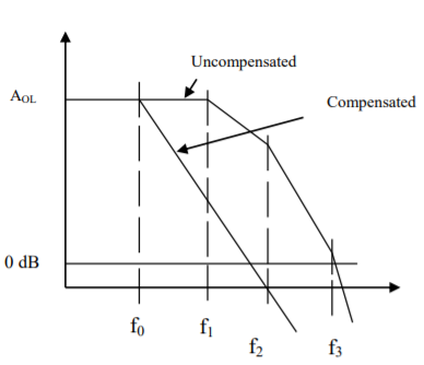
Fig: Pole Zero Compensation Response
As compared to the dominant pole compensation there is an improvement in bandwidth.
Q11) Explain Miller compensation of OpAmp?
A11) Miller Compensation Technique- Use of a capacitor feeding back around a high-gain, inverting stage
- Miller capacitor only.
- Miller capacitor with an unity-gain buffer to block the forward path through the compensation capacitor. Can eliminate the RHP zero.
- Miller with a nulling resistor. Similar to Miller but with an added series resistance to gain control over the RHP zero.
Miller Compensation of the Two-Stage Op Amp
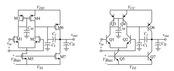
Fig: Miller Compensation
The various capacitors are
Cc = accomplishes the Miller compensation
CM = capacitance associated with the first-stage mirror (mirror pole)
CI = output capacitance to ground of the first-stage
CII = output capacitance to ground of the second-stage
Compensated Two-Stage, Small-Signal Frequency Response Model Simplified
Use the CMOS op amp to illustrate:
1.) Assume that gm3 >> gds3 + gds1
2.) Assume that gm3/CM >> GB
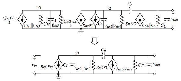
Fig: Small Signal Model
Same circuit holds for the BJT op amp with different component relationships.
General Two-Stage Frequency Response Analysis

Where:


The Nodal Equations are given by

And

Solving using Cramer’s Rule


Where

In General

 if
if


Q12) List the effects of negative feedback on non-linearity?
A12)
1) Gain Stabilization: The gain of a feedback system is almost entirely determined by the feedback path and not by the gain of the amplification path. This means that you can get predictable gains even when the gain of the amplification path is unknown or time-varying.
2) Distortion Reduction: High power amplifiers are often non-linear, e.g. Their gain decreases at high signal amplitudes. Since the gain of a feedback system does not depend much on the gain of the amplification path, the non-linearity has little effect.
3) Interference Rejection: External disturbances have little effect on the output of a feedback system because the feedback adjusts to compensate for them
4) Increases Circuit Stability
The output of an amplifier without negative feedback is affected by the variations in the temperature, frequency, or amplitude of the signal which further changes the gain of the amplifier and as result, we get a distorted signal in the output. Hence, the negative feedback is applied so that the gain of the amplifier is stabilized.
5) Increases Input Impedance/Resistance
The use of negative feedback increases the input impedance or resistance of the amplifier.
Z’in = Zin . (1 + β .Av)
6) Reduces Noise Level
The negative feedback which we apply to the amplifiers is in the opposite phase to that of the applied input signal, hence it cancels out the noises which are introduced in the output signal by the amplifier circuit. As a result, we get the output signal with a reduced noise level.
7) Improves Frequency Response & Bandwidth
The negative feedback which we apply to the amplifiers is a resistive network hence the gain of the amplifier with negative feedback is independent of signal frequency. As a result, the gain becomes constant over a wide range of signal frequencies in this way the frequency response of the amplifier with negative feedback is improved.
f’cf = fcf . (1 + β .Av)
Here f’cf = resultant cut-off frequency with negative feedback
fcf = cut-off frequency without feedback
Q13) Draw circuit and derive expression for Log amplifier using diode?
A13) As the name says it is an amplifier which produces the output proportional to logarithmic of the applied input. The log amplifier using op-amp is shown below. The input is applied through the inverting end of op-amp. As the non-inverting end has voltage zero then by virtual ground concept the voltage at inverting terminal also becomes zero.
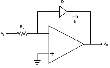
Fig: Log Amplifier
The equation for input voltage will be
 +If = 0
If = 
The current flowing through diode is given as

Here:
Is = Saturation Current
Vf = Voltage drops across diode in forward bias
VT = Thermal equivalent voltage
For feedback loop the KVL equation will be
0-Vf -V0 = 0
Vf = -V0
Substituting Vf in above equation of If

Equating both equations of If


Taking natural log of both sides we get


The above equations shows that the output is natural log of the applied input.
Q14) Explain the log amplifier circuit using transistor?
A14) In this configuration a transistor is placed in the feedback path of an op-amp wired in inverting mode. Collector of the transistor is connected to the inverting input of the op-amp, emitter to output and base is grounded. The necessary condition for a log amp to work is that the input voltage must be always positive. Circuit diagram of an Op-amp-transistor log amplifier is shown below.
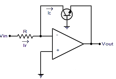
Fig: Log Amplifier using BJT
The base-emitter voltage of the transistor Vbe = -Vout ………(1)
We know that Ic = Iso (e(Vbe/Vt)-1) ………….(2)
Where Ic is the collector current of the transistor, Iso the saturation current, Vbe
The base emitter voltage and Vt the thermal voltage.
Equation (1) can be approximated as Ic = Iso e(Vbe/Vt) ………….(3)
i.e., Vbe = Vt In (Ic/Iso) …………….(4)
Since input pin of an ideal op-amp has infinite input impedance, the only path for the input current Ir is through the transistor and that means Ir = Ic.
Since the inverting input of the op-amp is virtually grounded
Ir = Vin/R
That means Ic = Vin/R ……………(5)
From equations (5) , (4) and (1) it is clear that
Vout = -Vt ln (Vin/IsoR1)………….(6)
Q15) Explain Antilog amplifier using diode?
A15) This device produces the output proportional to antilog of input. The inverting op-amp is used in this case as well. The figure below shows an antilog amplifier with its inverting terminal connected to the input end with diode and the non-inverting terminal is grounded.
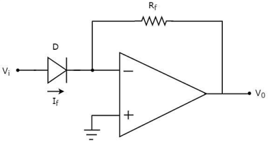
Fig: Antilog Amplifier using Diode
Applying KCL at input terminal we get


The current flowing through diode is given as

Substituting If in above voltage equation we get


At inverting terminal applying KVL we get


Substituting Vf in equation of V0 we get

The above equations shows that the output is natural antilog of the applied input.
Q16) Explain antilog amplifier using BJT?
A16) Basic Anti Log amplifier using transistor It is obtained by using a transistor as a diode in the input path of an op-amp as shown in the figure. The node B is at virtual ground, hence VB = 0. Thus, the collector and base are both at ground potential and VCB = 0. Hence the voltage across the transistor is VBE and we can write,

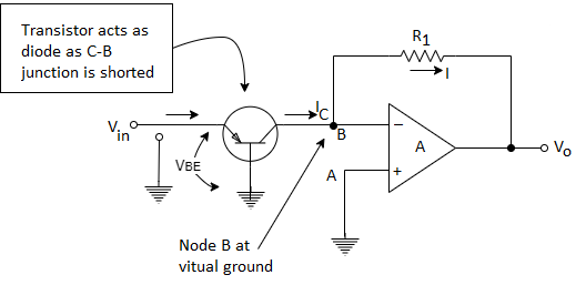
Fig: Antilog amplifier using Transistor
From the figure, VBE = Vin. Then

Now the current  and current I are same as op-amp input current is zero.


Let 

The output voltage is proportional to the exponential of Vin i.e antilog of Vin. Thus, circuit works as basic antilog amplifier. In both the above circuits it can be seen that the terms I0, Is and VT are present in the output equation. All these are the function of temperature. Hence, a temperature changes, these parameters also change and causes serious errors at the output.
Q17) How the log antilog amplifiers are affected by temperature? Draw and explain the temperature compensated circuits?
A17) For Log Amplifier the circuit has one problem. The emitter saturation current Is varying from transistor to transistor and with temperature. Thus, a stable reference voltage V ref cannot be obtained. This is eliminated by the circuit given below
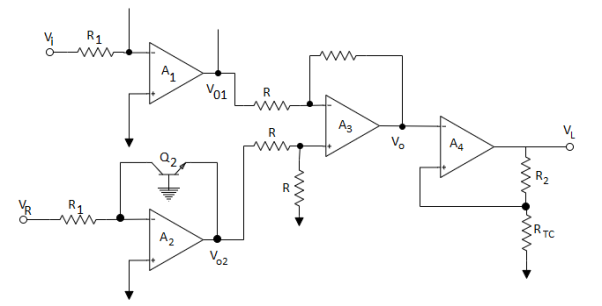
Fig: Log Amplifier with compensation of emitter saturation current
The input is applied to one log-amp, while a reference voltage is applied to one log-amp, while a reference voltage is applied to another log-amp. The two transistors are integrated close together in the same silicon wafer. This provides a close match of saturation currents and ensures good thermal tracking.
Assume IS1=IS2=IS
Thus, the reference level is now set with a single external voltage source. Its dependence on device and temperature has been removed. The voltage Vo is still dependent upon temperature and is directly proportional to T. This is compensated by the last op-amp stage A4 which provides a non-inverting gain of (1+R2/RTC). Temperature compensated output voltage VL

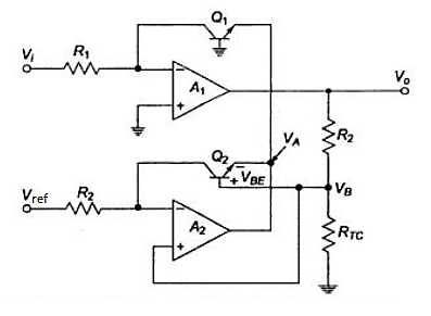
Fig: Logarithmic Amplifier using Two-Op-Amps
Where RTC is a temperature-sensitive resistance with a positive coefficient of temperature (sensor) so that the slope of the equation becomes constant as the temperature changes.
For Antilog Amplifiers temperature compensation is achieved by same technique.
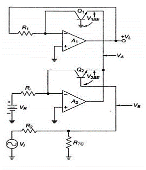
Fig: Antilog amplifier
 and
and  and
and


Therefore 
Rearranging we get


We know that
Therefore, 


Q18) What are sample and hold circuits also mention their need?
A18)
- The Sample and Hold circuit is an electronic circuit which creates the samples of voltage given to it as input, and after that, it holds these samples for the definite time. The time during which sample and hold circuit generates the sample of the input signal is called sampling time.
- Similarly, the time duration of the circuit during which it holds the sampled value is called holding time.
- Sampling time is generally between 1µs to 14 µs while the holding time can assume any value as required in the application.
- It will not be wrong to say that capacitor is the heart of sample and hold circuit.
- This is because the capacitor present in it charges to its peak value when the switch is opened, i.e during sampling and holds the sampled voltage when the switch is closed.
Need for Sample and Hold Circuits
If the input analog voltage of an ADC changes more than ±1/2 LSB, then there is a severe chance that the output digital value is an error. For the ADC to produce accurate results, the input analog voltage should be held constant for the duration of the conversion.
It is based on a sampling command and holds the output value at its output until the next sampling command is arrived.
The following image shows the input and output of a typical Sample and Hold Circuit.
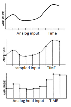
Fig: Input and output of S/H circuit
This sample and hold circuit consist of two basic components:
- Analog Switch
- Holding Capacitor
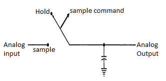
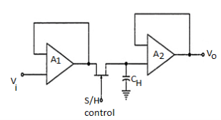
Fig: Open loop s/h circuit
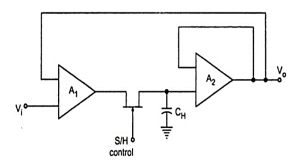
Fig: Closed loop s/h circuit
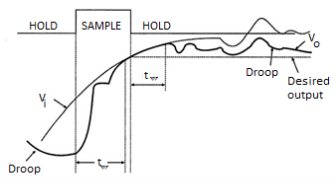
Fig: S/H characteristics
Acquisition Time (tac)
The time required for the charge in the holding capacitor to rise up to a level that is close to the input voltage during the sampling is called acquisition time. It is affected by three factors:
- The RC Time Constant
- The Slew-Rate of the Op-Amp
- The maximum output current of the Op-Amp
Aperture Time (tap)
The time delay between the initiation of VO tracking the Vi and the initiation of the hold command is called the Aperture Time. This delay is usually due to the propagation delays through the driver and the switch circuits.
For a precise timing operation, the hold command must be initiated in advance by an amount of aperture time.
Aperture Uncertainty (∆ tap)
The Aperture time will not be the same for all the sample and will vary from sample to sample. This uncertainty is called Aperture Uncertainty. This will severely affect the advancing of the hold command.
Hold Mode Settling Time (ts)
The hold mode settling time is the time taken by the output VO to settle within the specified error band (usually 1%, 0.1% or 0.01%) after the application of hold command.
Hold Step
During the switching from sample mode to hold mode, there might an unwanted transfer of charge between the switch and the holding capacitor (mainly due to the parasitic capacitances). This will affect the capacitor voltage as well as the output voltage. This change in the output voltage from the desired voltage is called Hold Step.
Feedthrough
Again, the parasitic capacitances in the switch may cause AC coupling between VO and Vi in hold mode. As a result, the output voltage may vary with changes in the input voltage and this is referred to as feedthrough.
Droop
Voltage Droop is a phenomenon where the voltage across the holding capacitor drops down due to leakage currents.
Advantages
- The main and important advantage of a typical SH Circuit is to aid an Analog to Digital Conversion process by holding the sampled analog input voltage.
- In multichannel ADCs, where synchronization between different channels is important, an SH circuit can help by sampling analog signals from all the channels at the same time.
- In multiplexed circuits, the crosstalk can be reduced with an SH circuit.
Q19) What are Zero crossing detectors?
A19) An op-amp detector that has the ability to detect the change from positive to negative or negative to a positive level of a sinusoidal waveform is known as a zero- crossing detector.
It is also known to be a square wave generator as the applied input signal is converted into a square wave by the zero -crossing detector.
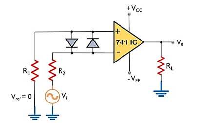
Fig: Zero crossing Detector
Here, the input signal Vi is provided to the inverting terminal of the op-amp while the non-inverting terminal is grounded by making use of two resistors R1 and R2.
It detects the point where the input signal crosses zero of the reference voltage level. For every crossing, the saturation level of the output signal changes from one to another.
The reference level is set at 0 and applied at the non-inverting terminal of the op-amp. The sine wave applied at the inverting terminal of the op-amp is compared with the reference level each time the phase of the wave changes either from positive to negative or negative to positive.
Firstly, when positive half of the sinusoidal signal appears at the input. Then the op-amp comparator compares the reference voltage level with the peak level of the applied signal.
Vo = Vref – Vi ---------------------------------------(1)
And we know the reference level is 0, thus
Vo = 0 – (+ Vsat) ----------------------------------------(2)
Therefore, Vo = - Vsat ---------------------------------(3)
During the negative half of the signal, thus the peak will have a negative polarity.
Again
Vo = Vref – Vi ---------------------------------------------(4)
Thus,
Vo = 0 - (- Vsat) --------------------------------------------------(5)
So, we get
Vo = + Vsat ---------------------------------------------(6)
In this way, the zero -crossing detector detects the change in the level of the applied signal.
Zero crossing detector is also known to be a square wave generator. As the output of the window comparator is nothing but a square wave.
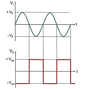
Fig: Input and output of zero crossing detector
V0 for the positive half of the applied signal is – Vsat,
This is the reason why we have achieved negative half of the square wave at the output when positive half of the sinusoidal signal is applied. While V0 for the negative half of the sinusoidal signal is + Vsat,
Applications:
- Phase Locked Loop
- Frequency counters and phase meters
Q20) Explain characteristics of comparator using op-amp?
A21)
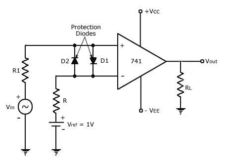
Fig: Comparator
- A reference voltage Vref of 1V is applied to the inverting terminal of op-amp.
- A time varying voltage Vin is applied to the non-inverting terminal of op-amp.
- Diode D1 and D2 are used to protect the op-amp from damage from excess amount of input voltage Vin.
- They are known as clamp diodes as they clamp the difference input voltage to +0.7V to -0.7V.
- Hence, the above circuit is called as non-inverting Comparator.
Characteristics of comparator
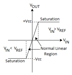
Fig: Voltage levels for comparator
- When Vin <Vref, then output Vo = -Vsat (≈ -Vee) because the voltage at negative input is higher than that of positive input.
- When Vin >Vref, then output Vo = +Vsat (≈ +Vee) as the positive input becomes positive with respect to the negative input.
- When Vin ≈ Vref, then Vo changes from one Vsat level to another.
- Therefore, the comparator is a type of analog to digital converter.
- It is also known as Voltage Level Detector because for a particular value of Vref, the voltage level of Vin can be detected.