Unit - 4
Digital Integrated Circuit Design
Q1) Design a CMOS digital circuit that realizes the Boolean function 
A1) Step1:
Design the PDN
First, we must rewrite the Boolean function as:
 =f(a, b, c)
In other words, write the complemented output in terms of un-complemented inputs
We must first complement this equation, and then apply DeMorgan’s Theorem


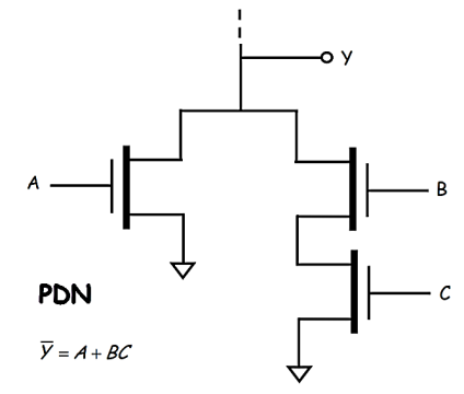
We can thus realize this logic with the following NMOS PDN
Step2: Design the PUN
First, we must rewrite the Boolean function as Y =f( ,
,  ,
,  )
)
In other words, write the un-complemented output in terms of complemented inputs.
Again, using DeMorgan’s Theorem


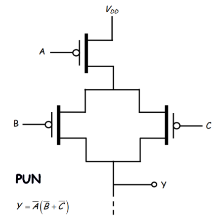
We can thus realize this logic with the following PMOS PUN
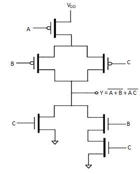
The complete CMOS design circuit will be
Q2) Design a gate that realizes this Boolean algebraic expression 
A2)
Step 1: Design PDN
First write Boolean Expression as


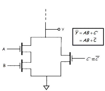
Thus, Y’= AB+C’
Therefore, the inputs to this logic gate should be A, B, and C’ (i.e, A, B, and the complement of C). Note that this Boolean expression “says” that: “The output is low if either, A AND B are both high, OR C’ is high” Of course another way of “saying” this is: “The output is low if either A AND B are both high, OR C is low” The PDN is therefore:
Step 2: Design the PUN
Note we have as similar problem as before—the expression for Y cannot explicitly be written in terms of complemented inputs A’ B’ and C’
Y= (A’+B’)C
“The output will be high if, either A OR B are low, AND C’ is low” Which is equivalent to saying: “The output will be high if, either A OR B are low, AND C is high” The CMOS digital logic device is therefore
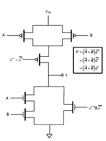
Q3) Draw the minimum CMOS transistor network that implements the functionality of Boolean equation F= ((A+B) C + D)'.
A3)
Using the above steps to realise the given Boolean function complete CMOS design we get is
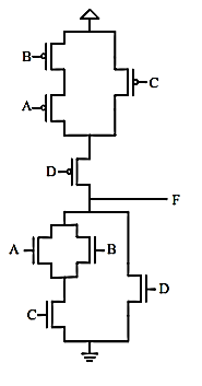
Q4) Draw the minimum CMOS transistor network that implements the functionality of Boolean equation F= (A (B C + D))'.
A4)
Using the above steps to realise the given Boolean function complete CMOS design we get is
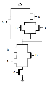
Q5) Draw the minimum CMOS transistor network that implements the functionality of Boolean equation F= (A +(B' + CD)')'.
A5)
F= (A +(B' + CD)')' = (A + B(CD)')' = (A + B (C' + D'))'
Using the above steps to realise the given Boolean function complete CMOS design we get is
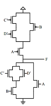
Q6) Draw the minimum CMOS transistor network that implements the functionality of Boolean equation F= (A' + B'C).
A6)
F = (A' + B'C) = ((A' + B'C)')'= (A (B'C)')' = (A (B + C'))'
Using the above steps to realise the given Boolean function complete CMOS design we get is
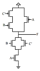
Q7) How to implement F = ab + bc + ca?
A7)

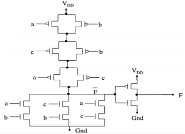
The above circuit shows the implementation.
Q8) Explain the difference between Latch and Flip Flop?
A8)
Latch | Flip-flop |
Latches are transparent devices i.e., when they are enabled, the output changes immediately if the input changes. | A transition from low to high or high to low of the clock signal will cause the flip-flop to either change its output or retain it depending on the input signal. |
A latch is a level Sensitive device(Level Triggering is involved). | A flip-flop is an edge sensitive device (Edge Triggering is involved). |
Latches are simpler to design as there is no clock signal (no careful routing of clock signal is required). | When compare to latches, flip-flops are more complex to design as they have clock signal and it has to be carefully routed. This is because all the flip-flops in a design should have a clock signal and the delay in the clock reaching each flip-flop must be minimum or negligible. |
The operation of a latch is faster as they do not have to wait for any clock signal. | Flip-flops are comparatively slower than latches due to clock signal. |
The power requirement of a latch is less. | Power requirement of a flip-flop is more. |
A Latch works based on the enable signal | A flip-flop works based on the clock signal |
Q9) Explain the CMOS logic basic structure?
A9)
The MOSFET (metal-oxide-semiconductor field-effect transistor) are of two types: PMOS (p-type MOS) and NMOS (n-type MOS).
A new type of MOSFET logic is made combining both the PMOS and NMOS processes and is called as complementary MOS (CMOS).
CMOS stands for “Complementary Metal Oxide Semiconductor”.
It is one of the most popular technology in the chip design industry and is used today to form integrated circuits for various applications.
Computer memories, CPUs and cell phones make use of this technology due to various advantages. This technology uses both P and N channel semiconductor devices.
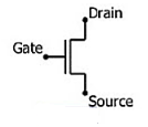
NMOS
NMOS is built on a p-type substrate with n-type source and drain diffused on it. Here, the majority carriers are electrons. When a high voltage is applied to the gate, the NMOS conducts and when low voltage is applied to the gate, it does not conduct. NMOS is faster than PMOS, as the carriers are electrons that travel twice as fast as the holes.
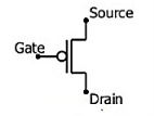
PMOS
P-MOS consists of P-type Source and Drain diffused on an N-type substrate. Here, majority carriers are holes. When a high voltage is applied to the gate, the PMOS does not conduct and when a low voltage is applied, it conducts. These devices are more immune to noise than NMOS devices.
CMOS Applications
- Computer memories, CPUs
- Microprocessor designs
- Flash memory chip designing
- Used to design application specific integrated circuits (ASICs)
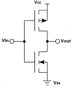
Fig: CMOS
The inverter circuit as shown in the figure above. It consists of PMOS and NMOS FET. The input A serves as the gate voltage for both transistors.
The NMOS transistor has an input from Vss (ground) and PMOS transistor has an input from Vdd. The terminal Y is output. When a high voltage (~ Vdd) is given at input terminal (A) of the inverter, the PMOS becomes open circuit and NMOS switched OFF so the output will be pulled down to Vss.
When a low-level voltage (<Vdd, ~0v) applied to the inverter, the NMOS switched OFF and PMOS switched ON. So the output becomes Vdd or the circuit is pulled up to Vdd.
INPUT | LOGIC INPUT | OUTPUT | LOGIC OUTPUT |
0 V | 0 | Vdd | 1 |
Vdd | 1 | 0 v | 0 |
Q10) Draw and explain CMOS realization of Inverter and AND gate?
A10) Inverter
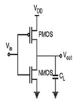
Fig: CMOS inverter
- It consists of PMOS and NMOS FET.
- The input A serves as the gate voltage for both transistors.
- The NMOS transistor has an input from Vss (ground) and PMOS transistor has an input from Vdd. The terminal Y is output.
- When a high voltage (~ Vdd) is given at input terminal (A) of the inverter, the PMOS becomes open circuit and NMOS switched OFF so the output will be pulled down to Vss.
- The truth table of inverter is:
A | Y = A’ |
0 | 1 |
1 | 0 |

Fig: NOT gate
AND Gate
As with the TTL NAND gate, the CMOS NAND gate circuit may be used as the starting point for the creation of an AND gate. All that needs to be added is another stage of transistors to invert the output signal.
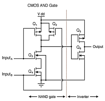
Q11) Draw and explain CMOS realization of NOR and NAND gate?
A11) NAND Gate
As with the TTL NAND gate, the CMOS NAND gate circuit may be used as the starting point for the creation of an AND gate. All that needs to be added is another stage of transistors to invert the output signal.
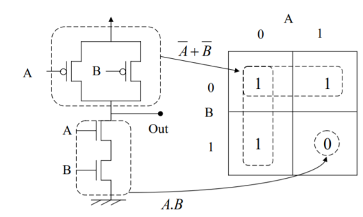
PDN connected to GND: 
PUN connected to 
NOR Gate
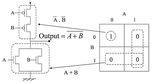
A CMOS NOR gate circuit uses four MOSFETs just like the NAND gate, except that its transistors are differently arranged. Instead of two paralleled sourcing (upper) transistors connected to Vdd and two series-connected sinking (lower) transistors connected to ground, the NOR gate uses two series-connected sourcing transistors and two parallel-connected sinking transistors like this
Q12) Explain CMOS implementation of SR latch using NOR gates?
A12) The simple two-inverter circuit alone has no provision for allowing its state to be changed externally from one stable operating model to the other. To allow such a change of state, we must add simple switches to the bistable circuit, which can be used to force or trigger the circuit from one operating point to the other Fig below shows the circuit structure of the simple CMOS SR latch, which has two such triggering inputs, S (set) and R (reset). In the literature, the SR latch is also called the SR flip-flop, since two stable states can be switched back and forth. The circuit consists of two CMOS NOR2 gates. The gate-level schematic of the SR latch.
The SR latch circuit has two complementary outputs, Q and Q . By definition, the latch is said to be in its set state when Q is logic “1” and Q is logic “0” (Inputs S=”1” and R=”0”). Conversely, the latch is in its reset state when Q is logic “0” and Q is logic “1” (Inputs S=”0” and R=”1”). When both inputs S and R are set to logic “0”, the SR latch. Will operate exactly like the simple cross-coupled bistable circuit (Fig. 5.2) and will hold either one of its two stable operating points (states) as determined by the previous inputs. The truth table of the NOR-based SR latch is summarized in Table. Note when both inputs S and R are equal to logic “1”, the output nodes will be forced to logic “0” which conflicts with the complementary of Q and Q’.
Therefore, this input combination is not permitted during normal operation and is considered to be a not allowed condition. The operation of the CMOS SR latch circuit of Fig. Below can be examined in more detail by considering the operating modes of the four nMOS transistors, M1, M2, M3 and M4. If the set input (S) is equal to VOH and the reset input (R) is equal to VOL, both the parallel connected transistors M1 and M2 will be on. Consequently, the voltage on node Q’ will become a logic-low level of VOL 0.
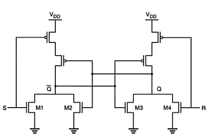
Fig: CMOS SR latch circuit based on NOR2 gate

Fig: Gate-level schematic and block diagram of the NOR-based SR latch.
 |  |  |  | Operation |
0 | 0 |  |  | Hold |
1 | 0 | 1 | 0 | Set |
0 | 1 | 0 | 1 | Reset |
1 | 1 | 0 | 0 | Not allowed |
Fig: Truth table of the NOR-based SR latch circuit
At the same time, both M3 and M4 are turned off, which results in a logic high voltage VOH at node Q. If the reset (R) is equal to VOH and the set input (S) is equal to VOL, the situation will be reversed (M1 and M2 turned off and M3 and M4 turned on). When both of the input voltages are equal to VOL, there are two possibilities depending on the previous state. Either M2 or M3 will be on, while both of the trigger transistors M1 and M4 are off. For transient analysis of the SR latch circuit is examined when a state changes. In this scenario, both the output nodes undergo simultaneous voltage transitions.
Thus, an interesting problem is to estimate the amount of time required for the simultaneous switching of the two output nodes. The exact solution of this problem requires solving two coupled differential equations, one for each output node. The problem can be simplified considerably if you assume that the two events take place in sequence rather than simultaneously. This assumption causes an overestimation of the switching time. To calculate the switching times for both output nodes, the total parasitic capacitance associated with each node must be calculated as


The circuit diagram of the SR latch is shown in Fig. Below together with the lumped load capacitances at nodes Q and Q’. Assuming that the latch is initially reset and that a set operation is being performed by applying S=”1” and R=”0”, the rise time associated with node Q can now be estimated as

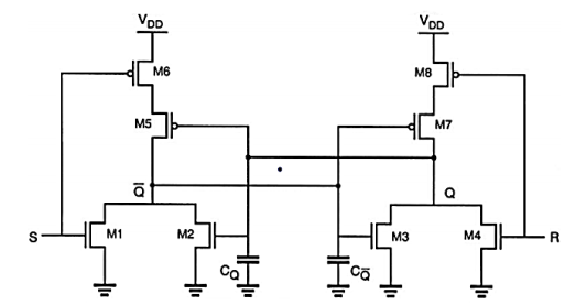
Fig: Circuit diagram of the CMOS SR latch showing the lumped load capacitances at both output nodes.
Q13) Explain CMOS implementation of SR latch using NAND gates?
A13) Fig. Below shows a SR latch using two NAND2 gates. Note in order to hold (preserve) a state, both of the external trigger inputs must be equal to logic “1”. The state of the circuit can be changed by pulling the set input or reset input to zero. The gate level schematic and the corresponding block diagram representation of the NAND-based SR latch are shown in Figure.
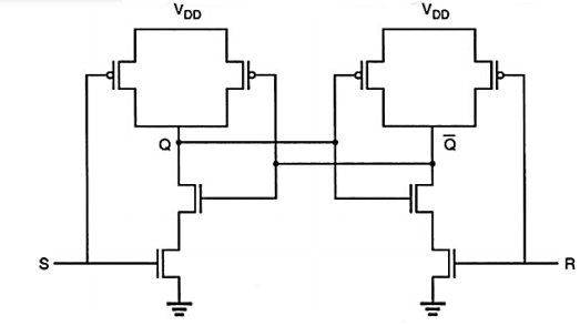
Fig: CMOS SR latch circuit based on NAND2 gates

S | R |  |
 | Operation |
0 | 0 | 1 | 1 | Not allowed |
0 | 1 | 1 | 0 | Set |
1 | 0 | 0 | 1 | Reset |
1 | 1 |  |
 | Hold |
Fig: Gate-level schematic and block diagram of the NAND based SR latch.
Note that a NAND-based SR latch responds to an active low input signals, while the NOR-based SR latch responds to an active high inputs. The small circles at the S and R input terminals indicate that the circuit responds to active low input signals. The truth table of the NAND SR latch is also shown in Fig. Above. The same approach used in the timing analysis of the NOR-based SR latches can be applied to NAND-based SR latches.
Q14) Explain CMOS implementation of clocked SR flip flop?
A14) The SR latches examined in the previous sections are essentially asynchronous sequential circuits, which respond to the changes occurring in input signals at a circuit-delay dependent time point during operation. To facilitate synchronous operation, the circuit response can be controlled simply by adding a gating clock signal to the circuit, so that the outputs will respond to the input levels only during the active period of the clock pulse. The gate-level schematic of a clocked NOR-based SR latch is shown in Fig. Below. Note if the clock (CK) is equal to logic “0”, the input signals have no influence upon the circuit response and the SR latch will hold its current state.
When the clock input goes to logic “1”, the logic levels applied to the S and R inputs are permitted to reach the SR latch. To illustrate the operation of the clocked SR latch, the waveforms of Fig. Below are provided. Note that the circuit is strictly level-sensitive during active phases (i.e. any changes occurring in the S and R input voltages when CK level is equal to logic “1” will be reflected onto the circuit outputs. Consequently, even a narrow spike or glitch occurring during an active clock phase can set or reset the latch, if the loop delay is shorter than the pulse width.
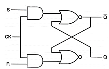
Fig: Gate-level schematic of the clocked NOR-based latch.
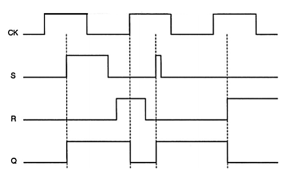
Fig: Sample input and output waveforms illustrating the operation of the clocked NOR-based SR latch circuit.
Fig. Below shows a CMOS implementation of a clocked NOR-based SR latch circuit, using two simple AOI (AND-OR-INVERT) gates. Notice that the AOI-based implementation of the circuit results in a very small transistor count, compared with the alternative circuit realization consisting of two AND2 and two NOR2 gates.
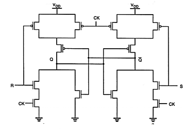
Fig: AOI (AND-OR-INVERT)-based implementation of the clocked NOR-based SR latch circuit.
The NAND-based SR latch can also be implemented by gating the clock input, as shown inbelow. For the implementation of Fig. Below, both the input signals S and R as well as the clock signal CK are active low. This means that in the input signal will be ignored when the clock is equal to logic “1” and that inputs will influence the outputs only when the clock is active (i.e. CK=”0”). For the circuit implementation of this clocked NAND-based SR latch, an OAI (OR-AND-INVERT) structure can be used, which is analogous to the AOI-based realization of the clocked NOR SR latch. A different implementation of the clocked NAND-based SR latch is shown below. Here, both input signals and the CK signal are active high. The drawback of this implementation is that the transistor count is higher than the active low version shown below.
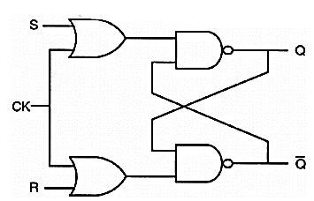
Fig: Gate-level schematic of the clocked NAND-based SR latch circuit, with active low inputs.

Fig (a) Gate-level schematic of the clocked NAND-based SR latch circuit, with active high inputs. (b) Partial block diagram representation of the same circuit.
Q15) Explain CMOS implementation of JK flip flop?
A15)

Fig: (a)Gate-level schematic of the clocked NAND-based JK latch circuit
Clocked JK Latch All simple and clocked SR latch circuits examined to this point suffer from the common problem of having a not-allowed input combination (i.e. their state becomes indeterminate when both S and R are activated at the same time. This problem can be overcome by adding two feedback lines from the outputs to the inputs, resulting in the JK latch (shown is Fig above). Fig. Below shows an all NAND implementation of the JK latch with active high inputs, and the corresponding block diagram representation.
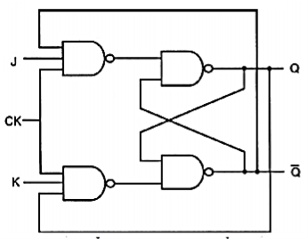
Fig: All-NAND implementation of the clocked JK latch circuit
J | K |  |
 | S | R |  |
 | Operation |
0 | 0 | 0 1 | 1 0 | 1 1 | 1 1 | 0 1 | 1 1 | Hold |
0 | 1 | 0 1 | 1 0 | 1 1 | 1 0 | 0 0 | 1 1 | Reset |
1 | 0 | 0 1 | 1 0 | 0 1 | 1 1 | 1 1 | 0 0 | Set |
1 | 1 | 0 1 | 1 0 | 0 1 | 1 0 | 1 0 | 0 1 | Toggle |
Fig: Table Detailed truth table of the JK latch circuit
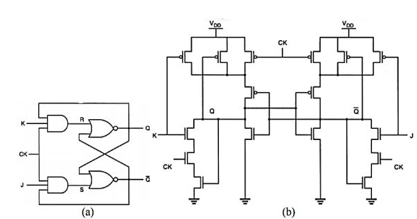
Fig: (a) Gate-level schematic of the clocked NOR-based JK latch circuit (b) CMOS AOI realization of the JK latch
The J and K inputs in this circuit correspond to the set and reset inputs of the basic SR latch. When the clock is active, the latch can be set with the input combination (J=”1”, K=”0”), and it can be reset with the input combination (J=”0”, K=”1”). If both inputs are equal to logic “0”, the latch preserves its current state. If both inputs are equal to logic “1” during the active clock phase, the latch simply switches its state due to the feedback. Thus, the JK latch does not have a not-allowed input combination. As in other clocked latch circuits, the JK latch will hold its current state when CK=”0”. The operation of the clocked JK latch is summarized in Table above. Fig. Above shows an alternative NOR-based implementation of the clocked JK latch, and the CMOS realization using the AOI circuit structure.
While there is not-allowed input combination for the JK latch, there is still a potential problem. If both inputs are equal to logic “1” during the active phase of the clock pulse, the output of the circuit will oscillate (toggle) continuously until either clock becomes inactive (CK goes to zero), or one of the input signals goes to zero. To prevent this undesirable timing problem, the clock pulse width must be made smaller than the input to-output propagation delay of the JK latch circuit (thus the clock signal must go low before the output has an opportunity to switch again, which prevents uncontrolled oscillation). This clock constraint is difficult to implement for most practical applications.
Q16) Explain CMOS implementation of D flip flop?
A16)
In general, direct CMOS implementations of conventional circuits such as clocked JK latch or the JK master-slave flip-flop tend to require a large number of transistors. This section examines specific versions of sequential circuits built primarily with CMOS transmission gates since they generally are simpler and require fewer transistors than the circuits designed with conventional structuring. As an example, consider the simple D-latch circuit shown in Fig. Below. The gate level representation of the D-latch is simply obtained by modifying the clocked NOR-based SR latch circuit. It can be seen from Fig. Below that the output Q assumes the value of the input D when the clock is active (i.e. for CK=”1”). When the clock signal goes to zero, the output will simply preserve its state. Thus, the CK input acts as an enable signal which allows data to be accepted into the D-latch.

Fig: Gate-level schematic and the block diagram view of D-latch
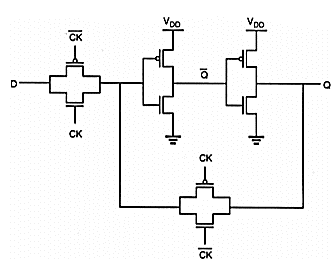
Fig: CMOS implementation of the D-latch (version 1)
The transistor implementation of a D-latch circuit can be realized as shown in Fig. Below. The figure shows a basic two-inverter loop and two CMOS transmission gate (TG) switches. The CMOS transmission gate (TG) consists of one nMOS and one pMOS transistor connected in parallel and acts as a bidirectional switch between nodes A and B which is controlled by signal C, as illustrated by Fig. Below.
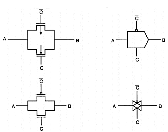
Fig: Four different representations of the CMOS transmission gate (TG)
The TG at the input is activated by the CK signal, whereas the TG in the inverter loop is activated by the inverse of the CK signal, (CK)’. Thus, the input signal is accepted (latched) into the circuit when the clock is high, and this information is preserved as the state of the inverter loop when the clock is low. The operation of the CMOS D-latch circuit can be better visualized by replacing the CMOS transmission gates with simple switches, as shown in Fig. Below. The timing diagram (Fig. Below) shows the time intervals during which the input and the output signals should be valid (unshaded).
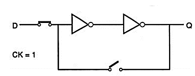
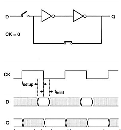
Fig: Simplified schematic and timing diagram, showing the setup and hold times.
Note that the valid D input must be stable for a short time before (setup time, setup t) and after (hold time, hold t) the negative clock transition, during which the input switch opens and the loop switch closes. Note that any violation of the setup and hold times can cause metastability problems which can lead to unpredictable transient behaviour.
Q17) Explain the Static behaviour of the two-inverter basic bistable circuit?
A17) In sequential logic circuits the output signals are determined by the current inputs as well as the previously applied input variables. Fig.(a) below shows a sequential circuit consisting of a combinational circuit and a memory block in the feedback loop. In most cases, the regenerative behaviour of sequential circuits is due to either a direct or an indirect feedback connection between the output and the input. Regenerative operation can, under certain conditions, also be interpreted as a simple memory function. Regenerative circuits can be classified into three main groups: bistable circuits, monostable circuits, and Astable circuits.
The general classification of non-regenerative and regenerative logic circuits is shown in Fig. Below. Bistable states have two stable states or operation modes, each of which can be attained under certain input and output conditions. Monostable circuits have only one stable operating point (state). Astable circuits have no stable operating point or state which the circuit can preserve for a certain time period. Among these main groups of regenerative circuit types, the bistable circuits are by far the most widely used and most important class. All basic latches flip-flops, registers and memory elements used in digital systems fall into this category.
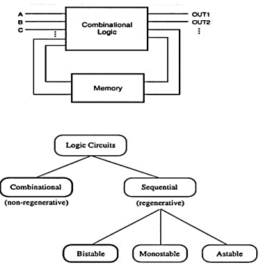
Fig: (a) Sequential circuit consisting of a combinational logic block and a memory block in a feedback loop (b) Classification of logic circuits based on their temporal behaviour
Behaviour of Bistable Elements
Fig.1(a) below shows an example of a bistable circuit which consists of two identical cross-coupled inverter circuits. Here the output voltage of inverter (1) is equal to the input voltage of inverter (2), (i.e. o1 i2 v v ), and the output voltage of inverter (2) is equal to the input voltage of inverter (1), (i.e. o2 i1 v v ). The voltage transfer characteristic of inverter (1) and (2) are plotted in Fig.(b). Notice that the input and output voltages of inverter (2) correspond to the output and input voltages of inverter (1), respectively. It can be seen that the two voltage transfer characteristics intersect at three points. The stable operating points of the circuit are labelled in Fig (b).
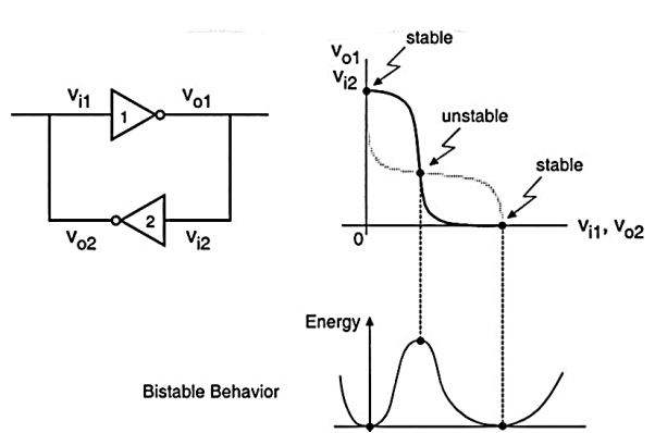
Fig: Static behaviour of the two inverter basic bistable circuit: (a) Circuit schematic (b) Intersecting voltage transfer curves of the two inverter, showing the three possible operating points. (c) Qualitative view of the potential energy levels corresponding to the three operating points
If the circuit is operating at one of these two stable points, it will preserve this state unless it is forced externally to change its operating point. Note that the gain of each inverter circuit, i.e., the slope of the respective voltage transfer curves, is smaller than unity at the two stable operating points. Thus, a significantly large external voltage perturbation must be applied so that the voltage gain of the inverter loop becomes larger than unity to change the state of the circuit.
The bistable behaviour of the cross-coupled inverter circuit can also be studied by examining the total potential energy levels at each of the three possible operating points (Fig. c). It can be seen that the potential energy is at its minimum at the two stable operating points, since the voltage gains of both inverters are equal to zero. The energy attains a maximum at the unstable operating point since the voltage gains of both inverters are its maximum.
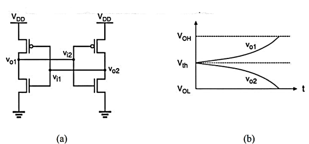
Fig: (a) Circuit diagram of a CMOS bistable circuit. (b) One possibility for the expected time domain behaviour of the output voltages, if the circuit is initially set at its unstable operating point.
Figure above shows the circuit diagram of a CMOS two-inverter bistable element. Note that at the unstable operating point of this circuit, all four transistors are in saturation, resulting in the maximum loop gain for the circuit. If the initial operating condition is set at this point, any small voltage perturbation will cause significant changes in the operating modes of the transistors. Thus, the output voltages of the two inverters will eventually diverge to VOH and VOL, respectively, as illustrated in Fig (b) above. The direction in which the output voltage diverges depends on the initial perturbation polarity