Unit - 3
Microprocessor Peripheral Interfacing
Q1) Explain the generation of I/O ports?
A1) When designing an I/O port, ensure that the port is only active when selected by the microprocessor
– Use latches (output) and buffers (input) to isolate the I/O port circuitry from the address and data bus
– Use the correct combinatorial logic circuitry and/or decoders with address bus to select the port.
• For 8-bit port IN AL, Port # OUT Port #, AL
MOV DX, Port # MOV DX, Port # I
N AL, DX OUT DX, AL
• For 16-bit port
IN AX, Port # OUT Port #, AX
MOV DX, Port # MOV DX, Port #
IN AX, DX OUT DX, AX
Since 8086/88 has a 16-bit data bus internally, it is capable of transferring 16-bit data to or from AX. Î This requires having two port addresses, one for each byte!
• Example: AX = 9876H, Port # = 40H OUT 40H, AX Î Port 40 Å 76H (AL), Port 41 Å 98H(AH) • For 8086, takes one bus cycle to complete the transfer, for 8088, two bus cycles are required
Q2) Explain programmable peripheral interface?
A2) The parallel input-output port chip 8255 is also called as programmable peripheral input-output port. The Intel’s 8255 are designed for use with Intel’s 8-bit, 16-bit and higher capability microprocessors. It has 24 input/output lines which may be individually programmed in two groups of twelve lines each, or three groups of eight lines. The two groups of I/O pins are named as Group A and Group B. Each of these two groups contains a subgroup of eight I/O lines called as 8-bit port and another subgroup of four lines or a 4-bit port. Thus, Group A contains an 8-bit port A along with a 4-bit port C upper.
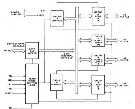
The port A lines are identified by symbols PA0-PA7 while the port C lines are identified as PC4-PC7 similarly. Group B contains an 8-bit port B, containing lines PB0- PB7 and a 4-bit port C with lower bits PC0-PC3. The port C upper and port C lower can be used in combination as an 8-bit port C. Both the port Cs is assigned the same address. Thus, one may have either three 8-bit I/O ports or two 8-bit and two 4-bit I/O ports from 8255. All these ports can function independently either as input or as output ports. This can be achieved by programming the bits of an internal register of 8255 called as control word register (CWR). The internal block diagram and the pin configuration of 8255 are shown in figs. The 8-bit data bus buffer is controlled by the read/write control logic. The read/write control logic manages all of the internal and external transfer of both data and control words. RD, WR, A1, A0 and RESET are the inputs, provided by the microprocessor to READ/WRITE control logic of 8255. The 8-bit, 3-state bidirectional buffer is used to interface the 8255 internal data bus with the external system data bus. This buffer receives or transmits data upon the execution of input or output instructions by the microprocessor. The control words or status information is also transferred through the buffer.
Q3) Explain the sample and hold circuit?
A3) Sample and Hold (S/H) Circuit
The signal that is fed to an A/D converter should be maintained constant during the conversion period
A S/H circuit samples the instantaneous value of the a.c. Signal and maintain it at a constant level
It makes this constant voltage available to A/D converter
Which requires a constant input during the conversion period LF398
LF198/LF298/LF398 are monolithic sample and hold circuits of National Semiconductor
They utilize BI-FET technology to obtain high accuracy, fast acquisition of signal and low droop rate
The droop rate is the rate at which the output of S/H circuit decreases
To make the output practically small this rate should be very small
An external capacitor known as hold capacitor is used with LF398
a droop rate as low as 5mV/min is obtained with a 1μF hold capacitor
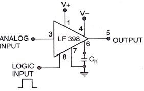
Description of LF398
Ch is a hold capacitor which is to be selected by the user, it is connected to pin 6
The logic is applied to pin 8, the logic is a pulse of height 5 V
Its width should be equivalent to acquisition time
When the logic is high, the input voltage is applied to the hold capacitor
The input voltage is off, when the logic goes low
Thus the hold capacitor holds the instantaneous value of the input voltage impressed upon it
LF398 operates at supply voltage ±5 Vd.c. To ±18Vd.c.
Q4) Explain analog multiplexer?
A4)
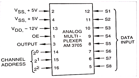
When a number of inputs are to be processed by the computer, an analog multiplexer is used
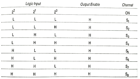
The multiplexer has a logic to switch on a particular desired channel A multiplexer may be of 8 channel or 16 channel
Any one of the inputs can be obtained by applying appropriate logic to the multiplexer
An analog multiplexer and A/D converter both are also available on a single I.C. Package
Ex: ADC0808 contains an 8-channel analog multiplexer and 8-bit A/D converter ADC0816 for 16-channel and 8-bit A/D converter.
Q5) Explain keyboard and display interface?
A5) Getting meaningful data from a keyboard requires three major tasks:
1. D e t e c t a k e y p r e ss
2. D e b o u n c e t h e k e y p r e s s .
3. Encode the keypress (produce a standard code for the pressed key).
Logic „0‟ is read by the microprocessor when the key is pressed.
Key Debounce: Whenever a mechanical push-bottom is pressed or released once the mechanical components of the key do not change the position smoothly; rather it generates a transient response. These may be interpreted as the multiple pressures and responded accordingly
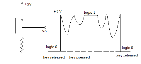
Figure.Mechanical key and its response
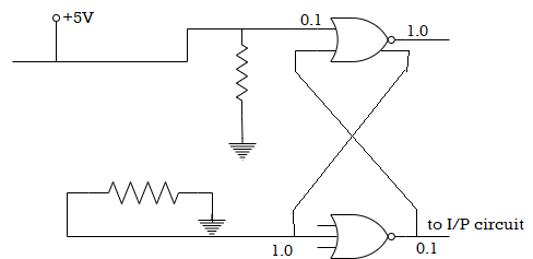
Figure. Hardware Debouncing circuit
The rows of the matrix are connected to four output Port lines, &columns are connected to four input Port lines. When no keys are pressed, the column lines are held high by the pull-up resistors connected to +5v. Pressing a key connects a row & a column.
To detect if any key is pressed is to output 0‟s to all rows & then check columns to see it a pressed key has connected a low (zero) to a column. Once the columns are found to be all high, the program enters another loop, which waits until a low appears on one of the columns i.e indicating a key press. A simple 20/10 msec delay is executed to debounce task. After the debounce time, another check is made to see if the key is still pressed. If the columns are now all high, then no key is pressed & the initial detection was caused by a noise pulse.
To avoid this problem, two schemes are suggested:
1. Use of Bistable multivibrator at the output of the key to debounce it.
2. The microprocessor has to wait for the transient period (at least for 10 ms), so that the transient response settles down and reaches a steady state. If any of the columns are low now, then the assumption is made that it was a valid key press. The final task is to determine the row & column of the pressed key &convert this information to Hex-code for the pressed key. The 4-bit code from I/P port & the 4-bit code from O/P port (row &column) are converted to Hex-code.
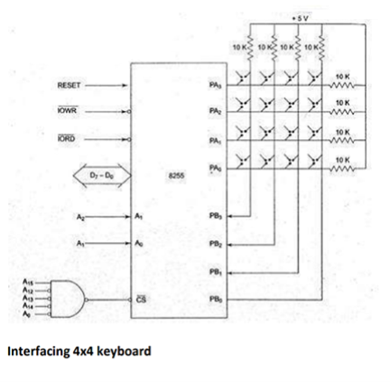
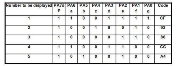
Display interface
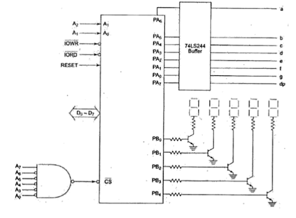
Q6) Explain keyboard matrix?
A6) The keyboard section consists of eight return lines RL0 – RL7 that can be used to form the columns of a keyboard matrix.
• It has two additional input : shift and control/strobe. The keys are automatically debounced.
• The two operating modes of keyboard section are 2-key lockout and N-key rollover.
• In the 2-key lockout mode, if two keys are pressed simultaneously, only the first key is recognized.
• In the N-key rollover mode simultaneous keys are recognized and their codes are stored in FIFO.
• The keyboard section also have an 8 x 8 FIFO (First In First Out) RAM.
• The FIFO can store eight key codes in the scan keyboard mode. The status of the shift key and control key are also stored along with key code. The 8279 generate an interrupt signal when there is an entry in FIFO. The format of key code entry in FIFO for scan keyboard mode is,
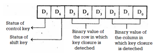
• In sensor matrix mode the condition (i.e., open/close status) of 64 switches is stored in FIFO RAM. If the condition of any of the switches changes then the 8279 asserts IRQ as high to interrupt the processor.
Q7) Explain the display section?
A7)
• The display section has eight output lines divided into two groups A0-A3 and B0-B3.
• The output lines can be used either as a single group of eight lines or as two groups of four lines, in conjunction with the scan lines for a multiplexed display.
• The output lines are connected to the anodes through driver transistor in case of common cathode 7- segment LEDs.
• The cathodes are connected to scan lines through driver transistors. • The display can be blanked by BD (low) line.
• The display section consists of 16 x 8 display RAM. The CPU can read from or write into any location of the display RAM.
Q8) Explain the Scan section?
A8)
• The scan section has a scan counter and four scan lines, SL0 to SL3.
• In decoded scan mode, the output of scan lines will be similar to a 2-to-4 decoder.
• In encoded scan mode, the output of scan lines will be binary count, and so an external decoder should be used to convert the binary count to decoded output.
• The scan lines are common for keyboard and display.
• The scan lines are used to form the rows of a matrix keyboard and also connected to digit drivers of a multiplexed display, to turn ON/OFF. CPU interface section:
Q9) Explain the CPU interface section?
A9) The CPU interface section takes care of data transfer between 8279 and the processor.
• This section has eight bidirectional data lines DB0 to DB7 for data transfer between 8279 and CPU.
• It requires two internal address A =0 for selecting data buffer and A = 1 for selecting control register of8279.
• The control signals WR (low), RD (low), CS (low) and A0 are used for read/write to 8279.
• It has an interrupt request line IRQ, for interrupt driven data transfer with processor.
• The 8279 require an internal clock frequency of 100 kHz. This can be obtained by dividing the input clock by an internal pre-scaler.
• The RESET signal sets the 8279 in 16-character display with two -key lockout keyboard modes..