Unit - 1
Study of Power Devices
Q1) An SCR has a breakover voltage of 400 V, a trigger current of 10 mA and holding current of 10 mA. What do you infer from it? What will happen if gate current is made 15 mA?
A1)
(i) Breakover voltage of 400 V. It means that if gate is open and the supply voltage is
400 V, then SCR will start conducting heavily. However, as long as the supply voltage is less than 400 V, the SCR stays open i.e. it does not conduct.
(ii) Trigger current of 10 mA. It means that if the supply voltage is less than breakover voltage (i.e. 400 V) and a minimum gate current of 10 mA is passed, the SCR will close i.e. starts conducting heavily. The SCR will not conduct if the gate current is less than 10 mA. It may be emphasised that triggering is the normal way to close an SCR as the supply voltage is normally much less than the breakover voltage.
(iii) Holding current of 10 mA. When the SCR is conducting, it will not open (i.e. stop conducting) even if triggering current is removed. However, if supply voltage is reduced, the anode current also decreases. When the anode current drops to 10 mA, the holding current, the SCR is turned off.
(iv) If gate current is increased to 15 mA, the SCR will be turned on lower supply voltage.
Q2) An SCR in a circuit is subjected to a 50 A surge that lasts for 12 ms. Determine whether or not this surge will destroy the device. Given that circuit fusing rating is 90 A2s.
A2) Circuit fusing rating = I2t = (50)2 × (12 × 10−3) = 30 A2s.
Since this value is well below the maximum rating of 90 A2 s, the device will not be destroyed.
Q3) An SCR has a circuit fusing rating of 50 A2 s. The device is being used in a circuit where it could be subjected to a 100 A surge. Determine the maximum allowable duration of such a surge.
A3) tmax = I2t (rating)/I2s = 50/(100)2 = 5x10-3 = 5ms
Q4) A 220Ω resistor is connected in series with the gate of an SCR. The gate current required to fire the SCR is 7mA. What is the input voltage (Vin) required to fire the SCR?
A4) The input voltage must overcome the junction voltage between the gate and cathode (0.7V) and also cause 7mA to flow through the 220Ω resistor. According to Kirchhoff’s voltage law, Vin is given by
Vin = VGK + IGR = 0.7V + (7mA) (220Ω) = 2.24V
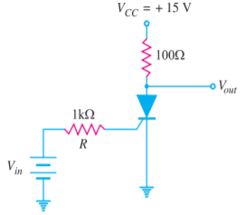
Q5) The SCR of Figure has gate trigger voltage VT = 0.7V, gate trigger current IT = 7 mA and holding current IH = 6 mA. (i) What is the output voltage when the SCR is off? (ii) What is the input voltage that triggers the SCR? (iii) If VCC is decreased until the SCR opens, what is the value of VCC?
A5)
(i) When the SCR is off (i.e. it is not conducting), there is no current through the 100Ω resistor.
∴ Vout = Supply voltage VCC = 15V
(ii) The input voltage Vin must overcome VT (=0.7V) and also cause 7 mA to flow through 1 kΩ resistor.
∴ Vin = VT + IT R = 0.7 + (7 mA) (1 kΩ) = 7.7V
(iii) In order to open the SCR, the VCC must be reduced so that anode current is equal to IH.
∴ IH = VCC - VT /100Ω
VCC = (100Ω) (IH) + VT = (100Ω) (6 mA) + 0.7 = 1.3V
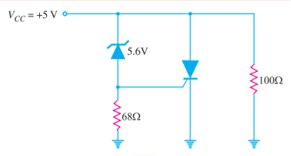
Q6) In Figure, the SCR has a trigger voltage of 0.7 V. Calculate the supply voltage that turns on the crowbar. Ignore Zener diode resistance.
A6)
The breakdown voltage of the Zener is 5.6V. To turn on the SCR, the voltage across 68Ω has to be equal to VT (= 0.7V).
∴ VCC = VZ + VT = 5.6 + 0.7 = 6.3V
When the supply voltage becomes 6.3 V, the Zener breaks down and starts conducting. The voltage VT (= 0.7V) across 68Ω forces the SCR into conduction. When the SCR conducts, the supply voltage is shorted by the SCR and the fuse in the supply voltage burns out. Thus, the load (100Ω) is protected from overvoltage.
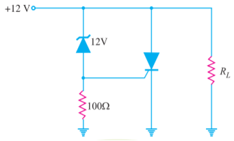
Q7) The Zener diode of Figure has a tolerance of ± 10% and the trigger voltage can be as high as 1.5V. What is the maximum supply voltage where crowbarring takes place?
A7)
The breakdown voltage of the Zener diode is 12V and it has a tolerance of ± 10%. It means that breakdown voltage of Zener can vary from 10.8V to 13.2V. Since the trigger voltage of SCR has a maximum value of 1.5 V
∴ Maximum value of supply voltage for crowbarring = 13.2V + 1.5V = 14.7V
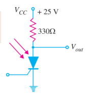
Q8) The circuit of Figure is in a dark room. When a bright light is turned on, the LASCR fires. What is the approximate output voltage? If the bright light is turned off, what is the output voltage?
A8)
Figure shows a light-activated SCR, also known as a photo-SCR. When light falls on the device, it starts conducting and the output voltage is ideally, Vout = 0V However, if we take into account anode-cathode drop, Vout = 0.7V. When light is turned off, the LASCR stops conducting and the output voltage is equal to the supply voltage VCC
Vout = VCC = + 25V
Q9) Give a simple method for testing an SCR?
A9)
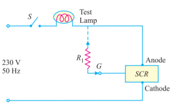
Figure shows a simple circuit for testing an SCR. The test lamp serves two purposes. First, it is a visual indicator of current conduction. Secondly, it limits current through the SCR.
(i) When switch S is closed, the lamp should not light for the SCR to be good. It is because voltage is applied only between anode and cathode but there is no trigger voltage. If the lamp lights, the SCR is shorted.
(ii) Now touch R1 momentarily between gate and anode terminals. For the SCR to be good, the lamp should light and continue to light. If it does not, the SCR is open. Note that the lamp will be on at half brilliance because the SCR conducts only every other half cycle.
Q10) Determine the input voltage necessary to cause the breakdown in SCR for 200 Ω resistance connected in series if the required gate current for firing is 6 mA.
A10)
In accordance to the given data and the reference diagram, it is mandatory to estimate the value of input voltage in such a manner that it should overcome the barrier voltage of 0.7 V.
Secondly, it should allow the current of 6 mA to flow through the resistor of about 200 Ω.
Hence, from the figure, the value of input voltage can be estimated as,
Input Voltage = Gate to Cathode Voltage + (Gate Current x Resistance)
Thus, Vin = VGC + IG R
= 0.7 +( 6 x 10-3 x 200 )
= 0.7 + (1200 x 10-3 )
= 1.9 V
Q11) Explain the construction and working of SCR?
A11)
- SCR is a solid state-operated device with the four-layered structure. The flow of current is in one direction just like a diode.
- It has three junctions along with the three terminals. The other name for SCR is Thyristor. These are the devices that are operated with the current.
- A large value of the current at the anode terminal is controlled by the value of the current applied at the terminal gate. Hence these are known as current-controlled devices.
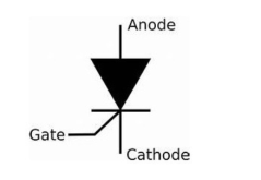
Figure. Symbolic Representation of SCR
- An SCR is constructed with four layers that consist of P-type and N-type semiconductor material. These are layered in such a way that it tends to form three junctions J1, J2, and J3. The three terminals that are attached to it are known as anode, cathode, and gate.
- The anode is the basic terminal through which the current flows or enters the device. The cathode is the terminal through which the entered current leaves the device.
- The current entering terminal is of positive polarity and the terminal through which the current is leaving is of negative polarity. In between the flow of current among the terminals, there must be a terminal that can provide the control. This can be provided by the terminal gate. This terminal is sometimes also referred to as the terminal of control.
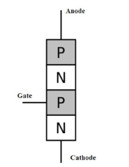
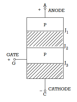
Figure. PNPN Type SCR
- Consider SCR of P-N-P-N type. In this structure the anode is connected at the above that is to P-type and the cathode is connected at the end that is for N-type, whereas the gate is connected to the p-type but it will be the second P-type in the sequence. Hence the gate terminal is positioned in such a way that it is nearer to the terminal cathode.
- In this, the junction J1 is formed in between the first P-type and the N-type. The second junction J2 will be lying in between N-type and the second P-type layers. The third junction will be in between the last P-type and the N-type layers. Based on the requirement or the necessity of the applications these layers of the Thyristor are doped. Silicon is preferred since it is intrinsic type.
Working:
- SCR starts conducting when it is forward biased, for this purpose the cathode is kept negative and anode positive. When a positive clock pulse is applied at the gate SCR is turned ON.
- Under forward biased condition J1 and J3 are forward biased and J2 is reverse biased. When clock pulse is applied at gate terminal J2 is forward biased and SCR starts conducting.
- SCR turns OFF and ON quickly. At OFF state SCR provides infinite resistance and in the ON state it offers low resistance may be in the range of 0.01 Ω to 1Ω.
Q12) With diagram explain the static characteristics of SCR?
A12)
Static Characteristic:
Figure shows the circuit diagram to obtain V – I characteristic of the SCR.
Here VAK is voltage between anode to cathode and Vg is gate voltage.
The static V – I characteristic of the SCR is divided into following mode.
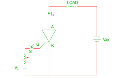
Figure. Circuit Diagram for V-I characteristics of SCR
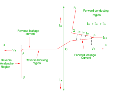
Figure. V-I characteristics of SCR
Reverse blocking mode
- When cathode is made positive with respect to anode and gate switch is kept open circuited, junction J1 and J3 are reverse biased whereas the junction J2 becomes forward biased.
- Hence only small leakage current flows through the device.
- If the anode voltage increases to certain level, an avalanche break down occurs at the junction J2 and current flows sharply through all the junctions.
- This current is limited to safe value to protect SCR due to high power dissipation.
- The region OA is known as forward blocking mode and AB is known as reverse avalanche breakdown mode of the SCR.
Forward blocking mode
- When anode is made positive with respect to cathode and switch S is kept open circuited, junction J1 and J3 are forward biased whereas the junction J2 become reverse biased.
- This will result in only small leakage current flows through the device.
Forward conducting mode
- When anode to cathode voltage increases to certain level say threshold voltage, an avalanche breakdown occurs at junction J2 and device comes into conduction state region PQ
- The voltage across SCR drops from several thousand voltage to few voltage and current increases sharply in the forward conducting state.
- When the gate signal is applied, SCR is turned on before forward break over voltage is reached.
- Higher the gate current, lower the forward break over voltage.
- Figure shows different value of gate current and corresponding break over voltage.
- Once the SCR conducts, it remains in conducting state despite gate signal removes.
- The SCR will turn off only when the forward current is reduced below holding current.
Q13) What are the dynamic characteristics of SCR explain?
A13) Dynamic characteristic
The switching action does not take place instantaneously, but it will take some finite time.
Turn on time (ton)
The turn on time of the SCR is defined as the time during which the SCR changes from forward blocking state to forward conducting state.
The total turn on time of the SCR is divided in to two intervals:
Delay time and Rise time
Ton = td + tr
Delay time (td)
It is time duration from the instant at which the gate current reaches 90% of its final value to the instant at which anode current reaches 10% of its final value.
Rise time (tr)
It is defined as time during which anode current rises from 10% to 90% of final value.
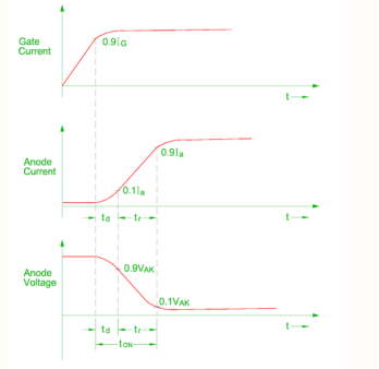
Figure. SCR turn on Waveforms
Turn off time (toff)
- Once the SCR start to conduct, gate loses control.
- The SCR can be turned off by reducing the anode current below holding current for sufficient time.
- This can be achieved by natural commutation or forced commutation.
- The turn off time of the SCR is defined as the time interval between the instant at which the anode current becomes zero and the instant at which SCR regain forward blocking voltage.
The total turn off time can be divided in to two intervals:
Reverse recovery time ( trr ) and gate recovery time ( tgr )
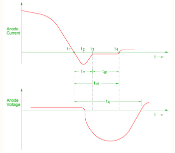
Figure. SCR turn-off waveforms
- The anode current becomes zero at instant t1.
- The anode current flows in the opposite direction during reverse recovery time t3 – t1.
- The reverse anode voltage developed across SCR at the instant t2 and reverse current continue to decrease.
- Therefore, the reverse recovery time is defined as the time between the current reversal and the instant at reverse current has decayed to 10% of negative peak value.
- The reverse recovery time increases as the forward current increases.
- When the reverse recovery current stops, high transient voltage appears across the SCR which may damage it.
- The middle junction J2 contains charges which must decay only by recombination at the end of reverse recovery time.
- This recombination is possible if a reverse voltage is maintained across the SCR therefore the time for recombination of charges ( t3 – t4 ) is called as gate recovery time tgr.
- The recombination is stopped at time t4 and forward voltage can be reapplied at time instant.
- The turn off time of the SCR is given is in the range of 3 to 100 micro- second.
- In practice circuit turn off time must be greater than SCR turn off time.
- Therefore, the circuit turn off time tc is defined as the time between the instant anode current becomes zero and at the instant reverse voltage becomes practically zero.
- The circuit turn off time tc must be greater than the SCR turn off time otherwise the SCR may turn on at undesired instant and it is known as commutation failure.
- The turn off time increases with increase in the magnitude of anode current and junction temperature.
- It also depends upon type of commutation circuit i.e. natural commutation or forced commutation.
Q14) Explain the major factors affecting the rating of SCR?
A14)
Thyristor ratings or SCR ratings are required for operating in safe zone. SCR has several ratings such as voltage, current, power, dv/dt, di/ dt , turn on time , turn off time and so on.
Anode voltage rating
This rating provides a brief picture about the withstanding power of thyristor in forward blocking mode in the absence of current.
Peak Working Forward Blocking
It specifies the maximum forward voltage (positive voltage applied across anode and cathode) that can be withstood by SCR at the time of working.
Peak Repetitive Forward Blocking Voltage:
It specifies the peak forward transient voltage that SCR can block repeatedly or periodically in forward blocking mode. This rating is specified at a maximum allowable junction temperature with gate circuit open.
During commutation process, due to high decreasing rate of reverse anode current a voltage spike Ldi/dt is produced which is the cause of VDRM generation.
Peak Non-Repetitive or Surge Forward Blocking Voltage (VDSM)
The peak value of forward transient voltage that does not appear periodically. This type of over voltage is generated at the time of switching operation of circuit breaker.
Peak Working Revere Voltage (VRWM)
It is the maximum reverse voltage which can be withstood by the thyristor repeatedly or periodically.
Peak Repetitive Revere Voltage (VRRM)
It is the value of transient voltage that can be withstand by SCR in reverse bias at maximum allowable temperature. This reason behind the appearance of this voltage is also same as VDRM.
Peak Non-Repetitive Revere Voltage (VRSM)
It implies the reverse transient voltage that does not appear repetitively. Though this voltage value is 130% of VRRM, it lies under reverse break over voltage, VBR.
Forward ON State voltage Drop (VT)
This is the voltage drop across the anode and cathode when rated current flows through the SCRat rated junction temperature. Generally, this value is lie between 1 to 1.5 volts.
Forward dv/dt Rating
When we apply a forward voltage to the thyristor Junction J1 and J3 are forward biased whereas junction J2 is reverse biased, hence it acts as capacitor. So due to C dv/dt at leakage current flows through the device. This value of current will increase with the value of dv/dt. The reason for leakage is the rate of voltage increasing.
The value of capacitance of the junction is constant hence when dv/dt increases to a suitable value that leakage current occurs and avalanche breakdown across junction J2. This value of dv/dt is called forward dv/dt rating which can turn on the SCR without the help of gate current.
Q15) List the factors affecting the current ratings of SCR?
A15) Current ratings of an SCR
The current carrying capability of an SCR is solely determined by the junction temperature. Some of the current ratings are
(i) Forward Current Rating.
The maximum value of anode current, that an SCR can handle safely without any damage, is called the forward current rating. The usual current rating of SCR’s is from 30A to100A.
In case the current exceeds the forward current rating, the SCR may get damaged due to intensive heating at the junctions.
(ii) On-state Current. When the device is in conduction, it carries load current determined by the supply voltage and load.
Onstate current is defined in terms of average and rms values. ITavis the average value of maximum continuous sinusoidal on state current frequency 40-60 Hz conduction angle 180 which should not exceed with intensive cooling.
(iii) Latching Current
It is the minimum device current which can be attained by the device before the gate drive is removed while turning on for conduction maintenance.
(iv) Holding Current.
It is the minimum on state current required to keep SCR in conducting state without any gate drive. Usually the value is 5mA
(v) Surge Current.
It is the maximum admissible peak value of a sinusoidal half cycle of 10 ms duration at a frequency of 50 Hz. The value is specified at a given junction temperature. During maximum surge on-state current the junction temperature exceeds temporarily, and forward blocking capabilities are lost for short period.
The maximum surge on-state current should occur occasionally.
(vi) I2t Value.
It is the time integral of the square of the maximum sinusoidal on-state current. This is usually specified for 3ms to 10ms and determines the thermal rating of the device.
(vii) Critical Rate of Rise of Current.
The maximum rate of increase of current during on-state which the Scr can tolerate is called critical rate of rise of current for the device. This the specified maximum junction temperature.
Q16) Explain R triggering of SCR?
A16) The turning on process of SCR is known as Triggering. This turns the SCR from Forward Blocking state to Forward conduction state is known Triggering.
R- Triggering
The figure shows simple method for varying the trigger angle for power in the load. Instead of using a gate pulse to trigger the SCR, the gate current is supplied by an AC source Es through Rmin, RVR and series diode D.
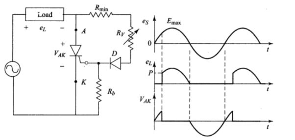
Figure. R-triggering
Operation:
- As Es goes positive, SCR becomes forward biased from anode to cathode. However, it will not conduct until gate current exceeds Ig(min).
- As Es forward biases the diode and SCRs gate-cathode junction it causes the flow of gate current ig.
- The gate current will increase as Es increases to its peak value. When
- Ig(min) the SCR turns on and El will approximately equals to Es.
- SCR remains “on” and eL=es decreases to the point where the lod current is below SCR holding-current. This happens close to the point until es=0 and begins to go negative.
- The SCR turns off and continues to remain off while es goes negative since its anode-cathode is reverse biased, since SCR is an open switch the load voltage is zero during this period.
- The purpose of diode in gate-circuit is to prevent the gate-cathode reverse bias from exceeding peak reverse gate voltage during negative half cycle of es.
- The diode is chosen to have peak reverse-voltage rating greater than the input voltage Emax.
- The same sequence is repeated when Es goes positive.
As shown in Figure the limiting resistor R(min) is placed between anode and gate so that the peak gate current of the thyristor gm is not exceeded.
In the worst case, that is when the supply voltage has reached its peak, Emax.

The stabilising resistor Rb should have such a value that the maximum voltage drops across it does not exceed maximum possible gate voltage Vg(max).
From the voltage distribution,

The thyristor will trigger when the instantaneous anode voltage, es, is

Q17) List the difference between Natural and Forced Commutation?
A17)
S.No | Natural Commutation | Forced commutation |
1 | Requires AC voltage at input | Requires DC voltage at input |
2 | External components are not required | External components are required |
3 | Used in controlled rectifiers, AC voltage controller | Used in choppers inverter etc. |
4 | SCR turns of due to negative supply voltage | SCR turns off due to current and voltage both |
5 | No power loss takes place during commutation | Power loss takes place during communication |
6 | Zero cost | Significant cost |
Q18) Draw the circuit and also sketch the waveform for class D commutation?
A18)
This is called as auxiliary commutation because it uses an auxiliary SCR to switch the charged capacitor.
In this, the main SCR is commutated by the auxiliary SCR. The main SCR with load resistance forms the power circuit while the diode D, inductor L and SCR2 forms the commutation circuit.
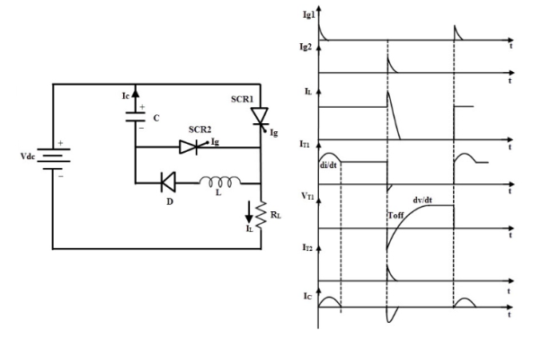
Figure. Class D commutation circuit
- When the supply voltage E is applied, both SCRs are in OFF state and hence the capacitor voltage is zero.
- For the capacitor to charge SCR2 must be triggered first. So, the capacitor charges through the path E+ – C+ – C- – SCR2- R- E-.
- When the capacitor is fully charged SCR2 becomes turned OFF because no current flow through the SCR2 when capacitor is fully charged fully.
- If SCR1 is triggered, current flows in two directions; one is the load current path E+ – SCR1- R- E- and another one is commutation current path C+ – SCR1- L- D- C.
- As soon as the capacitor completely discharges, its polarities will be reversed but due to the presence of diode the reverse discharge is not possible.
- When the SCR2 is triggered capacitor starts discharging through C+ – SCR2- SCR1- C-. When this discharging current is more than the load current the SCR1 becomes turned OFF.
- Again, the capacitor starts charging through the SCR2 to a supply voltage E and then the SCR2 is turned OFF. Therefore, both SCRs are turned OFF and the above cyclic process is repeated.
- This commutation method is mainly used in inverters as well as used in the Jones chopper circuit.
Q19) What is gate turn of thyristor explain with its working?
A19) GTO (gate turn-off) is like thyristor. It is a four layer, three junction P-N-P-N device like a standard thyristor. In this, the n+ layer at the cathode end is highly doped to obtain high emitter efficiency.
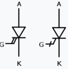
Figure. Symbol of GTO
Construction of GTO:
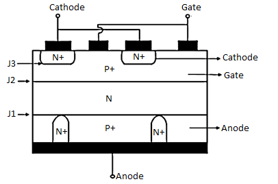
Figure. Structure of GTO
- Consider the structure of GTO which is similar to thyristor. It is a four layered structure which has three junctions P-N-P-N device. The n+ layer at the cathode end is highly doped to obtain high emitter efficiency.
- This results in the breakdown voltage of the junction J3 which I low and typically in the range of 20-40 volts.
- The doping level of p-type is highly graded because the doping level should be low to maintain high emitter efficiency whereas for having good turn OFF properties, doping of this region should be high.
- The gate and cathode should be highly interdigit with various geometric forms to optimize the current turn off capability.
- The junction between P+anode and N base is called anode junction.
- A heavily doped P+ anode region is required to obtain high efficiency anode junction so that good turn ON properties is achieved.
Principle of Operation:
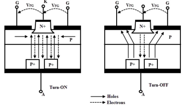
Figure. GTO operation
- When the anode terminal is made positive with respect to cathode by applying a positive gate current, the hole current injection from gate forward bias the cathode p-base junction.
- This results in the emission of electrons from the cathode towards the anode terminal. This induces the hole injection from the anode terminal into the base region. This injection of holes and electrons continuous till the GTO comes into the conduction state.
- To turn OFF a conducting GTO, a reverse bias is applied at the gate by making the gate negative with respect to cathode. A part of the holes from the P base layer is extracted through the gate which suppress the injection of electrons from the cathode.
- In response to this, more hole current is extracted through the gate results more suppression of electrons from the cathode. Eventually, the voltage drop across the p base junction causes to reverse bias the gate cathode junction and hence the GTO is turned OFF.
- During the hole extraction process, the p-base region is gradually depleted so that the conduction area squeezed. As this process continuous, the anode current flows through remote areas forming high current density filaments. This causes local hot spots which can damage the device unless these filaments are extinguished quickly.
- By the application of high negative gate voltage these filaments are extinguished rapidly. Due to the N base region stored charge, the anode to gate current continues to flow even though the cathode current is ceased.
- This is called a tail current which decays exponentially as the excess charge carriers are reduced by the recombination process. Once the tail current reduced to a leakage current level, the device retains its forward blocking characteristics.
Q20) Explain how using DIAC the TRIAC can be triggered?
A20)
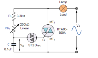
Figure. Triggering triac using diac
- When the AC supply voltage increases during the beginning of cycle, capacitor, C is charged through the series combination of the fixed resistor, R1 and the potentiometer, VR1 and the voltage across its plates increases.
- When the charging voltage reaches the breakover voltage of the diac, the diac breaks down and the capacitor discharges through the diac.
- The discharge produces a sudden pulse of current, which fires the triac into conduction.
- The phase angle at which the triac is triggered can be varied using VR1, which controls the charging rate of the capacitor. Resistor, R1 limits the gate current to a safe value when VR1 is at its minimum.
- Once the triac has been fired into conduction, it is maintained in its “ON” state by the load current flowing through it, while the voltage across the resistor–capacitor combination is limited by the “ON” voltage of the triac and is maintained until the end of the present half-cycle of the AC supply.
- At the end of the half cycle the supply voltage falls to zero, reducing the current through the triac below its holding current, IH turning it “OFF” and the diac stops conduction.
- The supply voltage then enters its next half-cycle, the capacitor voltage again begins to rise in the opposite direction and the cycle of firing the triac repeats over again.

Figure. Conduction