Unit - 4
DC to DC Converters
Q1) What is buck-boost converter?
A1)
It is basically a DC-DC converter which has output either low or high than the input voltage value. It is combination of a step up (Buck) and step up (Boost) converter. These devices have a diode connected with inductor and a capacitor. The input is connected to a solid-state device. The diode acts as a switch. The circuit shown below is of a buck-boost converter.

Fig: Buck-Boost Converter
The diode is in the reverse direction to the source. The capacitor and diode are in parallel to load. We use pulse width modulation to turn the controlled switch ON and OFF. Normally time based PWM is used as frequency based is difficult in implementation. This operates in two modes
i) When switch is ON, Diode is OFF:
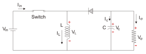
As seen from the above figure when the switch is ON it acts as a short circuit and hence, allows all the current to pass through it. In this condition the current flows through the switch and inductor and again to the input. The inductor stores energy at this time. When the switch is OFF the inductor reverses its polarity and then the current flows through the load and then diode and back to the inductor.
The total time period T = TON+TOFF
TON: ON time
TOFF: OFF time
The switching frequency fs= 1/T
In steady state Vin=VL
VL= L  = Vin
= Vin
Now duty cycle D= 
 =
= 
At end of ON state
 ILON =
  =
=  dt =
dt = 
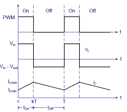
Ii) When switch is OFF, Diode is ON:
The circuit is shown below where the switch is in OFF state. The polarity of inductor is reversed. The current flows through the load resistance from the inductor and a step-up voltage is obtained at the output.
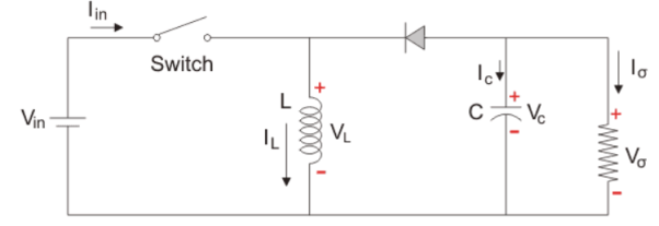
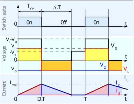
In this case VL=Vo
VL= L  = Vo
= Vo
 =
= 
TOFF= T-TON = T_DT = (1-D) T
 t= (1-D) T
 iL)open=
  (1-D) T
Q2) Explain 1-phase VSI?
A2)
The basic VSI generates ac output using semiconductor devices such as IGBT, MOSFET or BJT. The below circuit uses for pair of transistor diode acting as four switches. In case of resistive load current and voltage are in phase. In sinusoidal PWM half wave pulses are used. The width of each pulse is varied in proportion to the amplitude of sine wave.
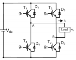
The above circuit has four switches and depending on their ON and OFF state we get the desired output. During first half of the sine wave g1 and g2 are ON the current flows through load using this path. This output holds for positive half cycle. In second half cycle g3 and g4 are ON remaining two are OFF. Now, the flow of current in this case through load is in opposite direction as in previous case.
Q3) Explain SPWM using VSI 1-phase?
A3)
The basic VSI generates ac output using semiconductor devices such as IGBT, MOSFET or BJT. The below circuit uses for pair of transistor diode acting as four switches. In case of resistive load current and voltage are in phase. In sinusoidal PWM half wave pulses are used. The width of each pulse is varied in proportion to the amplitude of sine wave
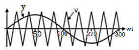
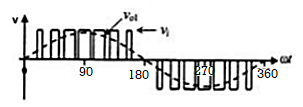
The gating pulses are generated by comparing and then applied to the switching devices.
VC= high frequency carrier wave
Vr= reference sinusoidal wave
Vo1=fundamental component of output voltage frequency
This technique is used to reduce the harmonic content of output voltage. In SPWM technique, the carrier signal is a high frequency triangular wave and it is compared with the reference sinusoidal signal. By comparing, the gating pulses are generated which are then applied to the switching devices.
Q4) What are 3-phase VSI?
A4)
It converts DC input into 3-phase ac output. The three-phase circuit is shown below.
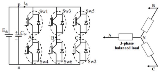
The inverter can be divided into two types due to conduction time of thyristors as:
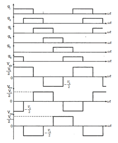
i) 120-degree mode of operation:
In this case at a time two thyristors are ON. They remain ON for 120o and then OFF. The A side is connected to positive and B to negative end. The phase voltages are equal to line voltages.
VAB=V
VBC=-V/2
VCA=-V/2
Ii) 180o mode of operation:
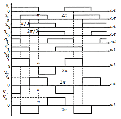
The devices here are conducting for 180o and are switched ON at 60o interval. The terminals of bridge A, B and C are connected to the three-phase star or delta of load.
For 0-60 S1, S5 and S6 will conduct. The terminals A and C are connected to positive of source and B is connected to negative of source. The load voltages will be
VAN=V/3
VBN=-2V/3
VCN=V/3
The line voltages are
VAB=VAN-VBN= V
VBC=VBN-VCN= -V
VCA=VCN-VAN= 0
Q5) A transistor dc chopper circuit (Buck converter) is supplied with power form an ideal battery of 100 V. The load voltage waveform consists of rectangular pulses of duration 1 ms in an overall cycle time of 2.5 ms. Calculate, for resistive load of 10 Ω. (a) The duty cycle γ. (b) The average value of the output voltage Vo. (c) The rms value of the output voltage Vorms. (d) The ripple factor RF. (e) The output dc power.
A5)
(a) 

(b) 


Q6) An 80 V battery supplies RL load through a DC chopper. The load has a freewheeling diode across it is composed of 0.4 H in series with 5Ω resistor. Load current, due to improper selection of frequency of chopping, varies widely between 9A and 10.2. (a) Find the average load voltage, current and the duty cycle of the chopper. (b) What is the operating frequency f ? (c) Find the ripple current to maximum current ratio.
A6)
(a) The average load voltage and current are

(a) The average load voltage and current are:


(b) To find the operating (chopping) frequency:
During the ON period, 
Assuming 

From eq (1)


But


Hence 
The maximum current  occurs at =1

Ripple current 

Q7) A DC Buck converter operates at frequency of 1 kHz from 100V DC source supplying a 10 Ω resistive load. The inductive component of the load is 50mH.For output average voltage of 50V volts, find: (a) The duty cycle (b) ton (c) The rms value of the output current (d) The average value of the output current (e) Imax and Imin (f) The input power (g) The peak-to-peak ripple current.
A7)
(a) 

(b) 

(c) 
(d) 
(e) 
(f) 

(g)
Q8) A Chopper circuit is operating on TRC at a frequency of 2 kHz on a 460 V supply. If the load voltage is 350 volts, calculate the conduction period of the thyristor in each cycle.
A8)

Chopping period 

Output voltage 
Conduction period of thyristor


Q9) Input to the step up chopper is 200 V. The output required is 600 V. If the conducting time of thyristor is 200 ssec. Compute Chopping frequency, If the pulse width is halved for constant frequency of operation, find the new output voltage.
A9)


Solving for T

Chopping frequency 
Pulse width is halved

Frequency is constant 

Output voltage 
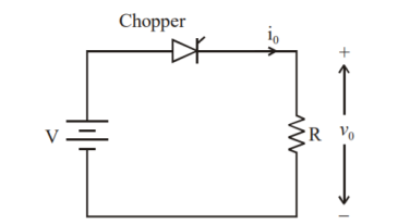
Q10) A dc chopper in figure has a resistive load of and input voltage of V = 200 V. When chopper is ON, its voltage drop is 2 V and the chopping frequency is 1 kHz. If the duty cycle is 60%, determine Average output voltage RMS value of output voltage Effective input resistance of chopper Chopper efficiency.
A10)
 Cho[[er voltage drop,
Average output voltage


RMS value of output voltage


Effective input resistance of chopper is


Output Power:


Input Power:


Chopper efficiency


Q11) A chopper feeding on RL load is shown in figure, with V = 200 V, R = 5, L = 5 mH, f = 1 kHz, d = 0.5 and E = 0 V. Calculate – Maximum and minimum values of load current. – Average value of load current. – RMS load current. – Effective input resistance as seen by source. – RMS chopper current.
A11)


Chopping period is 
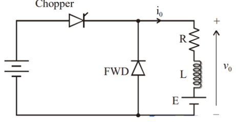
Maximum value of load current is given by


Minimum value of closing current is given by


Average value of load current is

For linear variations of current

RMS load current is given by


RMS chopper current is given by

Effective input resistance is

 Average source current


Therefore effective input resistance is

Q12) A dc chopper has a resistive load of 20Ω and input voltage VS = 220V. When chopper is ON, its voltage drop is 1.5 volts and chopping frequency is 10 kHz. If the duty cycle is 80%, determine the average output voltage and the chopper on time.
A12)


 Voltage drop across chopper =1.5 volts
Average output voltage

 =0.80(220-1.5)=174.8 volts

Chopping period


Chopping ON time


Q13) In a dc chopper, the average load current is 30 Amps, chopping frequency is 250 Hz, supply voltage is 110 volts. Calculate the ON and OFF periods of the chopper if the load resistance is 2 ohms.
A13)

Chopping period 


Chopper ON period,

Chopper OFF period,


Q14) The single-phase half-bridge transistor inverter shown in Fig. Below has a resistive load of R = 3Ω and the d.c. Input voltage Vdc = 60 V. Determine:
(a) The rms value of the output voltage.
(b) The rms value of the load voltage at the fundamental frequency.
(c) The output power.
(d) The average and peak current of each transistor.
(e) The peak reverse blocking voltage VBR of each transistor.
(f) The total harmonic distortion factor.
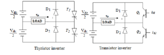
A14)
(a) the rms value of the output voltage is

(b) the rms value of the load voltage at the fundamental frequency is

(c) The output power is

(d) The avereage and peak current of each transistor are

Because each transistor conducts for a 50% duty cycle, the average current of each transistor is

(e) the peak reverse blocking voltage  of each transistor is

(f) The total harmonic distortion factor is

Q15) For the single-phase MOSFET bridge inverter circuit shown below, the source Vdc =125 V, load resistance R =10 Ω and output voltage frequency fo = 50 Hz.
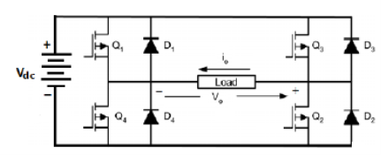
a) Draw the output voltage and load current waveforms.
(b) Derive the rms value of the output voltage waveform and hence calculate the output power Po in terms of the output voltage.
(c) Analyse the amplitude of the Fourier series terms of the output voltage waveform by considering up to the 7th order harmonic. Determine the value of the rms output voltage in terms of harmonics rms values.
(d) Calculate the average and peak currents of each transistor.
(e) Estimate the total harmonic distortion factor THD of the circuit.
A15)
(a)

(b) The rms value of the output voltage is


(c) The Fourier series of the output voltage is

The amplitude  of the nth harmonic is


Hence the output voltage Fourier representation is,

In terms of the harmonics

This value is less than  since we calculate up to 7th order harmonics only.
(d) Since the duty cycle of each transistor is 0.5, the current waveform is as shown below
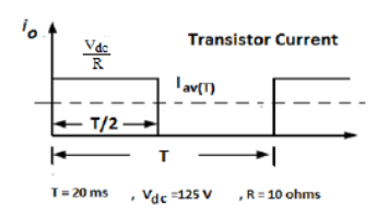

Peak current

(e)the total harmonic distortion factor


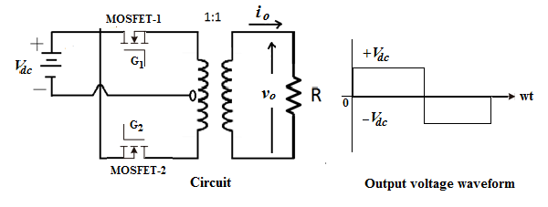
Q16) A single-phase MOSFET parallel inverter has a supply d.c. Voltage of 100V supplying a resistive load with R =10 Ω via a center-tap transformer with 1:1 ratio. The output frequency is 50 Hz.
(a) Draw the circuit diagram and the output voltage waveform of the inverter.
(b) Determine the rms value of the output voltage waveform.
(c) Determine the amplitude of the Fourier series terms for the square output voltage waveform up to 9th order harmonics.
(d) Calculate the rms value of the output voltage in terms of harmonic components that obtained in (b).
(e) Determine the power absorbed by the load consider up to 9th order harmonic.
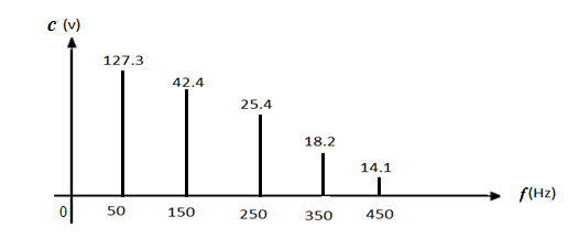
(f) Draw the frequency spectra of the output voltage waveform.
(g) Calculate the total harmonic distortion factor THD.
A16)
(a) the circuit diagram and the output voltage waveform of the inverter
(b) The rms value of the output voltage is

(c) the Fourier series of the output voltage is

The amplitude cn of the n th order harmonic is:


Hence the output voltage Fourier representation is,

(d) In terms of the harmonics, the rms value of the output voltage is
 =97.974V
(e) To calculate the power we most calculate the rms value of the current for each harmonic the amplitude of the nth harmonic current

Where 

The total power is 
 |  |  |  |  |  |
1 | 50 | 127.3 | 10 | 12.73 | 810 |
3 | 150 | 42.4 | 10 | 4.24 | 89.8 |
5 | 250 | 25.5 | 10 | 2.55 | 32.5 |
7 | 350 | 18.2 | 10 | 1.82 | 16.5 |
9 | 45- | 14.1 | 10 | 1.41 | 9.99 |
(f) The frequency spectrum is given in Fig.
(g) The total harmonic distortion factor


This is very high THD, the practical value of THD is about (3-10)% hence we need to use low-pass filter at the output to filter out most of the undesirable harmonic component and to produce nearly sinusoidal output waveform.
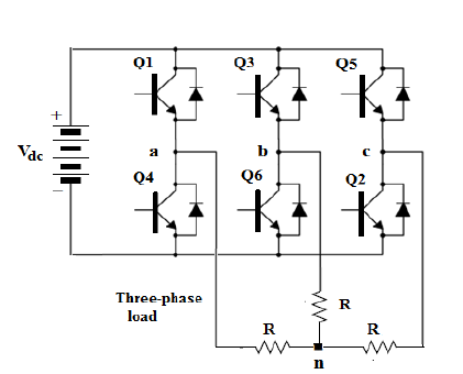
Q17) The three-phase inverter in Fig. Shown used to feed a Y-connected resistive load with R =15 Ω per-phase. The d.c. Input to the inverter Vdc = 300 V and the output frequency is 50 Hz. If the inverter is operating with 120˚ conduction mode, calculate: (a) The peak and rms value of the load current IL, (b) The output power, and the average and rms values of the current of each transistor.
A17)
(a) For 120ᵒ conduction mode, at any time the load resistances of two phases are connected in series, hence, peak value of load current is

The rms value of the phase voltage is

Hence the rms value of the load current is

(b) The load power is

(c) For 120ᵒ conduction mode, each transistor carries current for (1/3)rd of a cycle, hence the average transistor current is

The rms value of the thyristor current is

Q18) A half-controlled single-phase bridge rectifier is supplying an R-L load. It is operated at a firing angle a and the load current is continuous. The fraction of cycle that the freewheeling diode conducts is?
A18)
The circuit of a single-phase half controlled bridge rectifier with RL load and free wheel diode is shown as below.
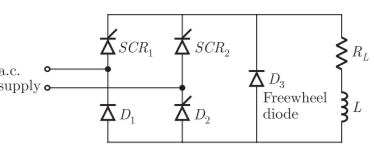
The voltage current wave forms are as shown below
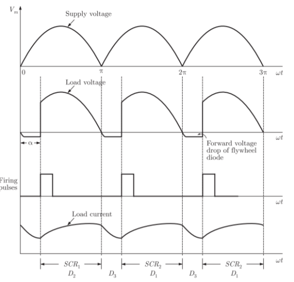
We note that, for continuous load current, the flywheel diode conducts from π to π+α in a cycle. Thus, fraction of cycle that freewheel diode conducts is α/π.
Thus fraction of cycle that freewheel diode conducts is a α/π.
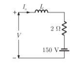
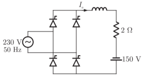
Q19) A single phase fully controlled converter bridge is used for electrical braking of a separately excited dc motor. The dc motor load is represented by an equivalent circuit as shown in the figure. Assume that the load inductance is sufficient to ensure continuous and ripple free load current. The firing angle of the bridge for a load current of I0 = 10 A will be?
A19)
Here for continuous conduction mode, by Kirchoff’s voltage law average load current


