Unit - 5
Power Devices Protection and Circuits
Q1) List the need of resonant converters?
A1) Need for Resonant Converters
- The pulse-width modulated DC-DC and DC-AC converter topologies are the controllable switches that are operated in a switch mode where they are needed to start and completely turn off the strain during each switching.
- In the switch mode procedure, the switches are put through high switching stresses and high switching power loss that increases linearly along with the switching regularity for the PWM.
- Another drawback regarding the switch mode procedure may be the EMI produced due to large di/dt and dv/dt triggered by a switch mode procedure.
- These shortcomings of the switch mode converters are exacerbated if the switching frequency is increased, also and/or the existing that you could reduce steadily the converter size and weight in order to increase the power density.
- Therefore, to realize high switching frequencies in converters, the shortcomings is minimized if each switch into the converter changes its status from on to down and vice versa whenever the voltage through it is zero at the switching instant. This is termed zero voltage switching and zero present switching appropriately.
- Thus, size and weight of converter reduces, and hence reduce cost and gratification improves to great level across it. The converter topologies and switching methods which end in zero voltage and/or zero switching that is present some form of LC resonance, these are broadly categorized as "resonant converter"
- The fundamental purpose of the switches inside the resonant converters to make a wave that is square or ac waveform from the dc supply and resonating inductor and capacitor (LC) remove undesired harmonic components from the square wave.
- There are two techniques that are main in a resonant converters . First the switch produces a wave that is square that is applied to series LC circuit .It is known as a show resonant converter. Next the switch generates a revolution that is square of that is positioned for a synchronous LC circuit. It is called a resonant converter that is parallel.
- The manufacturing with this converter are provided towards force or maneuvered further for the specified production example DC-DC,DC-AC transformation using converters which are mainstream shown in figure.
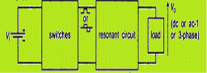
Fig(a)

Fig(b)
Q2) Explain the concept of zero current switching resonant converters?
A2)
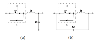
- In a zero crossing resonant switch an inductor Lr is connected in series with a power switch S in order to achieve zero-current-switching (ZCS). The resonant switch is said to operate in half-wave mode, when the switch is allowed to resonate in the positive half cycle only.
- If the diode is connected in anti-parallel with the unidirectional switch , the switch current can flow in both directions. In this case the resonant switch can operate in full wave mode.
- At turn-on, the switch current will rise slowly from zero and then oscillate because of the resonance between Lr and Cr.
- Finally, the switch can be commutated at the next zero current duration. The objective of this type of switch is to shape the switch current waveform during conduction time in order to create a zero current condition for the switch to turn-off.
- Thus the switches of ZCS resonant converters turn OFF and ON at zero current. The resonant circuit consists of a switch S, inductor L and capacitor Cr as shown in the figure.
- The inductor Lr is connected in series with power switch S to achieve ZCS.
- It is classified into two types
- L-type
- M-type
- The inductor limits di/dt of the switch current and Lr and Cr constitutes the series resonant circuit.
Q3) Explain the concept of zero voltage switching resonant converters?
A3)
- Zero voltage switching can be defined as conventional square wave power conversion during the switch’s on-time with resonant switching transitions.
- It can be considered as square wave power utilizing a constant off-time control which varies the conversion frequency or on-time to maintain regulation of the output voltage.
- Regulation of the output voltage is accomplished by adjusting the effective duty cycle performed by varying the conversion frequency, changing the effective on-time in ZVS design.
- Zero-voltage switching: transistor turn-on transition occurs at zero voltage. Diodes may also operate with zero-voltage switching.
- Zero-voltage switching eliminates the switching loss induced by diode stored charge and device output capacitances
- Zero-voltage switching is usually preferred in modern converters.
- Zero-voltage transition converters are modified PWM converters, in which an inductor charges and discharges the device capacitances. Zero-voltage switching is then obtained.
Q4) Explain difference between EMI and EMC?
A4) Electromagnetic Interference (EMI): The degradation in the performance of a device due to the fields making up the electromagnetic environment Electromagnetic Compatibility (EMC): The capability of electrical and electronic devices to operate in their intended electromagnetic environment without suffering or causing unacceptable degradation as a result of EMI EMI is the lack of EMC. EMI requirements
1) Source that generates noise
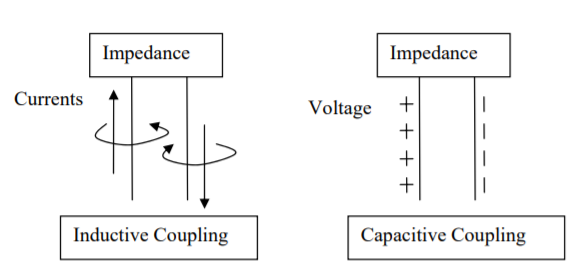
2) Coupling path to transmit the noise
- Radiated
- Conducted
3) Receptor that is susceptible to noise.

Interference Sources
1. Lightning-rapid current pulse creates spectrum from Hertz to 100 MHz
2. Electrostatic Discharge (ESD)
3. Power Disturbances
4. Power Supplies
5. Wireless devices
6. Computers
7. Computer peripherals
8. Fluorescent lights
9. Car ignition systems Less expensive to take action at the design phase to reduce EMI then to correct problem in post production.
Non-ideal behavior of passive circuit elements (wires, resistors, capacitors and inductors) is modeled using parasitic circuit elements. These are unintentional resistance, inductance and capacitance that adversely affect component performance.
Q5) What is soft switching and explain the sources of EMI?
A5) Semiconductors utilized in Static Power Converters operate in the switching mode to maximize efficiency. Switching frequencies vary from 50 Hz in a SCR based AC-DC Phase Angle Controller to over 1.0 MHz in a MOSFET based power supply. The switching or dynamic behavior of Power Semiconductor devices thus attracts attention specially for the faster ones for a number of reasons: optimum drive, power dissipation, EMI/RFI issues and switching-aid networks. With SCRs’ 'forced commutation' and 'natural (line) commutation' usually described the type of switching. Both refer to the turn-off mechanism of the SCR, the turn-on dynamics being inconsequential for most purposes. A protective inductive snubber to limit the turn-on di/dt is usually utilized. For the SCRs’ the turn-off data helps to dimension the 'commutation components' or to set the 'margin angle'. Conduction losses account for the most significant part of total losses. Present day fast converters operate at much higher switching frequencies chiefly to reduce weight and size of the filter components. As a consequence, switching losses now tend to predominate, causing the junction temperatures to rise. Special techniques are employed to obtain clean turn-on and turn-off of the devices. This, along with optimal control strategies and improved evacuation of the heat generated, permit utilisation of the devices with a minimum of deration.
Soft switching
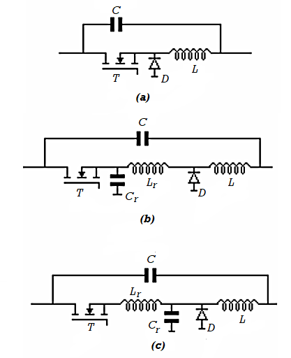
Fig (a)Hard Switch (b) ZVS (c) ZCS
Reduction of size and weight of converter systems require higher operating frequencies, which would reduce sizes of inductors and capacitors. However, stresses on devices are heavily influenced by the switching frequencies accompanied by their switching losses. It is obvious that switching-aid-networks do not mitigate the dissipation issues to a great extent. Turn-on snubbers though not discussed, are rarely used. Even if used, it would not be able to prevent the energy stored in the junction capacitance to discharge into the transistor at each turn-on. Soft switching techniques use resonant techniques to switch ON at zero voltage and to switch OFF at zero current. There are negligible switching losses in the devices, though there is a significant rise in conduction losses. There is no transfer of dissipation to the resonant network which is non-dissipative. The two basic configurations are as shown in Figure above.
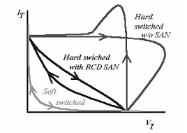
The switching trajectory in the voltage-current plane of a device is illustrated in Figure above comparing the paths for that of a Hard-switched operation without any SAN, a Hard-switched with a R-C-D Switching-Aid-Network and a resonant converter. It is indicative of the stresses and losses. A designer would prefer the path to be as close as possible to the origin.
Q6) What are the techniques to minimize EMI in industrial environments?
A6) In most of the dynamic industrial environments, electronic devices, signal and power wiring, and other electrical plant/process equipment often interact to create noise or electromagnetic interference (EMI) problems which can degrade critical measurement and control signals.
Proper grounding and shielding techniques can help reduce or eliminate these problems and maintain signal integrity.
There are three basic elements required in order for the noise problem to exist;
- A noise source to generate the noise,
- A receiving device which is affected by the noise,
- A coupling channel between the source and receptor.
The objective in electromagnetic compatibility is to minimize, divert, or eliminate one of the three elements necessary for a noise problem.
Capacitive Coupling
- Any piece of plant equipment or wiring which can develop an electric charge, or potential, can be expressed as a voltage. If the charge changes, then a changing electric field is generated which can couple capacitively to other equipment or wiring.
- Capacitively coupled noise can be modeled as a current as shown in Figure . This type of noise is dominant when a circuit or termination has high impedance because the noise voltage generated at the receiver is the noise current, in, times the receiver impedance, Zin.
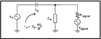
Fig. Capacitive coupling equivalent circuit
- An easy and effective way to minimize capacitively coupled interference is to use cable shielding. The shield is a Gaussian or equi-potential surface on which electric fields can terminate and return to ground without affecting the internal conductors.
Shielding techniques for EMI
- EMI Shielding puts impedance discontinuity to the path of a propagating radiated EM wave, either reflecting it or absorbing it.
- When an incident noise hit a shield, some portion of it will be reflected, absorbed and pass through with an attenuated magnitude. In a good shield, a weak noise wave can pass through.
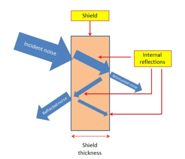
- The effectiveness of a shield depends on the three factors; reflections, absorption and multiple reflections. Reflection means an instant reflection of incident wave when hit a shield surface. Multiple reflections include internal reflections and re-reflections of waves or noise.
EMI Shielding Effectiveness Equation
SEdB = RdB + AdB + MdB
Where;
SEdB – Shielding effectiveness
RdB – Reflection loss
AdB – Absorption loss
MdB – Multiple reflections
- In far field, reflection loss is the predominant shielding mechanism at the lower frequencies while at higher frequencies absorption loss is dominant.
- For near field electrical sources, reflection loss is the predominant at the lower frequencies while absorption loss is predominant at higher frequencies.
- For near field magnetic sources, absorption loss is the predominant mechanism at all frequencies.
EMI Shielding Techniques
- Volumetric Shielding:
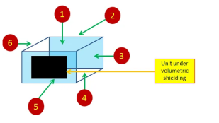
This is a type of shielding unit, sub-assembly, product or device by covering in all six sides, literally, by covering a box. This is also known as “Faraday Cage”. This is effective in most cases
The drawback is cost and thermal performance for high power application as the area bounded or covered will have poor air circulation.
- Nested Shielding
- Nested Shielding is an EMI shielding using different levels of shield material. Each level is not necessarily a volumetric shield; it can be a low cost and simple shield.
- However, since there are several layers of shields, this technique has become effective and even more cost friendly than a single layer sophisticated shield.
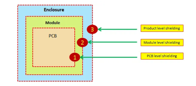
PCB Level Shielding:
PCB shielding is specific to PCB modules. In some cases, shielding in the enclosure level is unable to address EMI on the PCB level, whereas concentrating on the specific portion of the PCB will totally solve the issue. This is a common practice in SMPS wherein design engineers are hunting which part of the PCB is radiating or conducting noise then simply tried to shield that area.
Q7) List the various standards of EMI and EMC?
A7) To minimize EMI, devices need to have EMC. Devices that are electromagnetically compatible can prevent the worst effects of EMI without interfering with the device’s functioning or the operation of other devices. EMC standards ensure that a device does not generate EMI, is not affected by EMI, and that the device’s operation does not disturb the communication system around it. Additionally, EMC standards standardize testing procedures for measuring EMI so that repeatability and comparison grounds are established for measurements.
To keep compliance with EMC standards, manufacturers implement EMI reduction techniques—like proper grounding, EMI filtering, or product EMI shielding—to keep EMI within acceptable limits.
Application | Common EMC Standard(s) | Significance |
Medical | IEC 60601-1-2 | This standard regulates the safety and performance of medical equipment and systems under electromagnetic environments |
Automotive | SAE, | ISO7637, IEC CISPR-25, ISO114501, ISO1145-2 |
Military | ,IL-STD-461, DEF STAN 59/411, MIL-STD-704, MIL-STD-1275, MIL-STD-1399 | Regulates the electromagnetic emissions and susceptibility of the systems used in military applications. |
Industrial | FCC Part 15 Class A, EN 61000-6-4(generic), EN 61000-6-2(generic) | A general set of EMC standards for regulating the intentional, unintentional or incidental radiations for devices used in commercial, industrial or business environments. |
Commercial | FCC Part 15 Class B, EN 61000-6-3(generic), EN 61000-6-1(generic) | Devises the immunity requirements for electrical and electronic equipment used in commercial, pubic, light industrial or residential locations. |
Switchgear and control | EN/IEC 60947-1 | Regulates low-voltage switch gears and control geas with working voltages within 1500 V DC and 1000 V AC |
Power station and substation | IEC TS 61000-6-5 | Sets the immunity levels for the equipment utilized in the generation, transmission and distribution of electricity. |
Process control and measurement | EN/IEC 61326-1 | Specifies the immunity and emissions levels of electrical equipment or devices with a working potential less than 1000 Vac and 1500 V DC. |
Application | Common EMC Standard(s) | Significance |
Medical | IEC 60601-1-2 | This standard regulates the safety and performance of medical equipment and systems under electromagnetic environments |
Automotive | SAE, | ISO7637, IEC CISPR-25, ISO114501, ISO1145-2 |
Military | ,IL-STD-461, DEF STAN 59/411, MIL-STD-704, MIL-STD-1275, MIL-STD-1399 | Regulates the electromagnetic emissions and susceptibility of the systems used in military applications. |
EMI Standards
The EMI (Electromagnetic Interference) standard was originally created to protect electronic circuits from electromagnetic interference that may prevent them from performing the way they were originally designed to be. These interferences might sometime even make the device completely malfunction that it might become dangerous to users. It first became a concern in the 1950’s, and was primarily of interest to the military due to a few notable accidents arising from navigation failures due to Electromagnetic interference in navigation systems, and radar emissions leading to inadvertent weapons release. As such the military wanted to ensure systems were compatible with one another and the operations of one does not affect the other as that could lead to fatalities in their craft.
Asides military applications, recently advancements in Medicine and Health related solutions like Pacemakers and other kind of CIEDs, have has also contributed to the need for EMI regulations as interference in devices like this could lead to life threatening situations.
These among other scenarios are what lead to the establishment of the EMI interference standard and with the large number of EMC regulatory bodies that have been established.
Q8) What are isolation transformers? Explain its importance?
A8) Isolation transformer does not convert any voltage levels. The Primary voltage and the secondary voltage of an isolation transformer always remain the same. This is because the primary and the secondary winding ratio is always equal to the 1. That means the number of turns in primary and secondary winding is same in isolation transformer.
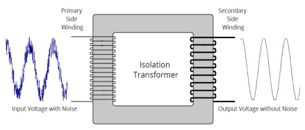
It is very important to use isolating transformers when an oscilloscope measures signals in an electrical circuit which is not galvanically isolated from the network. Because the current circuit can be closed (short-circuited) between oscilloscope common point and grounding. The main purpose of the isolation transformer is safety and protection of electronic components and the persons against electrical shock. It physically separates the power supplying from primary side and a secondary side circuit connected to electronic components and grounded metal parts which are in contact with the person. Basically, the transformer secondary side is isolated from the grounding.
The isolation transformer is used to isolate the primary and secondary. As discussed previously, the transformer does not have any electrical connections between primary and secondary, it is also used as an isolation barrier where the conduction happens only with the magnetic flux. It is used for safety purpose and to cancel noise transfer from primary to secondary or vice-versa.
When the isolation transformer is designed it is very important to pay attention to windings capacitance values which create capacitive coupling. This enables AC signal to pass from primary to the secondary side which significantly increased the noise level. For this purpose, the windings are surrounded by a metal strip which is grounded (creating a Faraday shield).
The isolation transformers are used as instrument transformers when the high voltage should be measured. The high voltage is dangerous for the person who tries to measure high voltage but it can also harm the measurement circuits. In this case, the step-down isolation transformer is used to reduce the high voltage to the safe level and for measurement range.
Q9) How EMI can arise in different ways. List all of the possible ways?
A9) Electromagnetic interference is the interference caused by an electromagnetic disturbance affecting the performance of a device, transmission channel, or system. It is also called radio frequency interference, or RFI, when the interference is in the radio frequency spectrum.
EMI - Electromagnetic Interference can arise in many ways and from a number of sources. The different types of EMI can be categorized in a number of ways.
One way of categorizing the type of EMI is by the way it was created:
- Man-made EMI: This type of EMI generally arises from other electronics circuits, although some EMI can arise from switching of large currents, etc.
- Naturally occurring EMI: This type of EMI can arise from many sources - cosmic noise as well as lightning and other atmospheric types of noise all contribute.
Another method of categorizing the type of EMI is by its duration:
- Continuous interference: This type of EMI generally arises from a source such as a circuit that is emitting a continuous signal. However, background noise, which is continuous, may be created in a number of ways, either manmade or naturally occurring.
- Impulse noise: Again, this type of EMI may be man-made or naturally occurring. Lightning, ESD, and switching systems all contribute to impulse noise, which is a form of EMI.
The sources of EMI can be broadly classified into two groups:
- Natural sources
Ex: Lightning
- Manmade sources
Ex: Commercial radio and telephone communications
We classify them as
Functional: EMI can originate from any source designed to generate electromagnetic energy which can create interference as normal part of its operation.
Incidental: EMI can originate from man-made sources. These sources are not designed specifically to generate electromagnetic energy but which do infact cause interference.
Natural: EMI can be caused by natural phenomena such as electrical storms , rain particles , solar and interstellar radiation.
Q10) What are various cooling techniques and heat sink design?
A10) Cooling and heat sinks
- Heat sink is a thermal device, which is conductive in nature. It is a metallic device, which increases the effective dissipation area of a surface and therefore increases the rate of heat dissipation when compared to the rate of generation.
- It is designed to absorb and remove heat from an object like Computer, mobile phones, DVD players and fridges. It removes heat from object or circuit, and sends them to surrounding medium.
- Heat sinks consist of fan or cooling device to disperse heat from another object. In computers, it is attached with a microprocessor chip to absorb heat and sends it to air. Heat sinks are made of metals like copper or aluminum alloy
Heat Sink are of two types:
- Active Heat Sink
- Passive Heat Sink
Active Heat Sink
- When the heat sink utilizes fan (HSF) it is active heat sink. In most of computer processor, a fan is attached just above the heat sink.
- This utilizes power for cooling process. Active heat sinks are used in liquid cooling system.
Passive Heat Sink
- When the heat sink does not utilize a fan, it is passive heat sink. They do not have any mechanical component, which makes them more reliable.
- These heat sinks are made of aluminum-finned radiator. They dissipate heat through principle of convection. Proper and steady airflow is maintained between the fins, to attain full stability of the device.
Passive Cooling
This type of cooling uses radiation or convection methods for heat transfer by using heat sink or heat spreader. For architectural designs, natural resources like soil or wind act as heat sink for heat absorption. This helps for better performance of the electronic devices within the operating temperature.
Active Cooling
This type of cooling depends on external devices for heat transfer. The mode of heat transfer is convection, which helps to increases the fluid flow for more heat removal. Additional components like fans are used when natural convection is not sufficient to remove heat. This type is used in electronics, hard drives and CPU for heat removal.
Q11) What is Snubber circuit? Derive the condition required for snubber circuit?
A11) Snubber Circuits are the one’s used for suppressing voltage spikes. These are energy absorbing circuits. Normally, the voltage spike occurs due to the inductor present in the circuit. Most basic form of snubber circuit is the RC snubber circuit. Below shows the figure of the snubber circuit having resistor and capacitor in series.
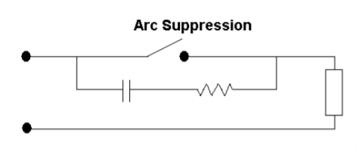
Designing
We take our first assumption as the circuit is having negligible impedance. The value of peak current in the circuit will be calculated using the relation

Where:
Vo= It is the value of Open circuit voltage
Rs =It is the value of Snubber Resistance
The rate of change of voltage w.r.t time is calculated as

From above two equations we can write

The value of energy in capacitor is given as

According to Ohm’s Law
R=Vo/I
I = switching current
Vo= open circuit voltage
The energy dissipated in the snubber circuit will be equal to the energy dissipated by the capacitor. Because of this the value of the capacitor is selected such that the resistor will dissipate half of the wattage rating of the resistor.


Where:
f= Value of switching frequency
2f= Transitions/ cycle
Condition for snubber circuit
Firstly, the energy stored in the circuit capacitor should be > energy stored in the circuit inductance.


Where:
Vo= open circuit voltage
I = Value of closed circuit current
L= Inductance
Secondly, for the snubber circuit the time constant should be < 10% of the ON time.

Where:
TON= shortest on-time expected
R = snubber resistance
C = snubber capacitance
Q12) What are the conditions for causes of over current fault in power circuits?
A12) Most of the thyristor circuit are fast operating which can be controlled in such way to prevent the load current from rising too high to cause circuit damage where the current can rise out of control to many times the normal rated value, and steps have to be taken to limit these conditions and to protect the other circuit components against the effects of the high current.
Cause of over current fault condition
An over current can occur due to any of the following cause:
(i) Output short-circuits.
(ii) Internal faults thyristor circuit.
(iii) Inversion failure in naturally commutated circuits.
(iv) Commutation failure in a forced commutation circuits, and
(v) Short circuit between one of the phases of mains and the bridge.
Over current Protection
The over current protection for the conductors and the connected load can only be provided by a fuse or circuit breaker installed at the point where the circuit originates or where it receives its supply.
If an OCPD is located downstream from the supply, then the over current protection is technically subdivided with short-circuit, ground-fault protection located upstream, as well as separate overload protection located downstream. The fuses or circuit breakers located downstream provide full over current protection for any circuits or equipment located on their load side while providing only overload protection for their line- or supply-side circuit.

Fig. Split over current protection for transformer circuit.
Q13) List the Ideal characteristics of an over voltage protection circuit?
A13) Ideal characteristics of an over voltage protection circuit
- To prevent excess voltage from being applied to the components.
- The protection circuit should not interfere with the normal function of the system or circuit. The protection circuit should not load the power supply and cause related voltage drops.
- The protection circuit should be able to distinguish between normal voltage fluctuations and harmful over-voltage.
- The OVP method should not to have false trips or undetected real over-voltage conditions. This can be a nuisance in the case of false trips and also dangerous if it is unable to see the real over-voltage conditions.
- There are various protection circuit designs, each with its merits, mode of operation, sensitivity, ability, and reliability. The protection can either clamp off the excess voltage, or completely shut down the power supply.
Q14) How over voltage conditions occur in power supply and how we can protect the devices from this condition?
A14) An over-voltage condition might occur in the power supply due faults inside the supply, or from external causes such as those in the distribution lines.
The magnitude and duration of the over-voltage are some of the major considerations when designing an effective protection. The protection involves setting a threshold voltage above which the control circuit shuts down the supply or diverts the extra voltage to other parts of the circuit such as capacitor.
Overvoltage Protection:
Over voltage protection is a feature of power supply which shuts down the supply, or clamps the output, when the voltage exceeds a preset level.
Most power supplies use an over-voltage protection circuit to prevent damage to the electronic components. The impact of an over-voltage condition varies from one circuit to the other and ranges from damaging the components to degrading the components and causing circuit malfunctions or fire.
The over voltage protection circuit may be constructed using discrete components, integrated circuits, mechanical devices such as relays, etc. These can either connected internally or externally depending on the circuits involved.
Ideal characteristics of an over voltage protection circuit
- To prevent excess voltage from being applied to the components.
- The protection circuit should not interfere with the normal function of the system or circuit. The protection circuit should not load the power supply and cause related voltage drops.
- The protection circuit should be able to distinguish between normal voltage fluctuations and harmful over-voltage.
- The OVP method should not to have false trips or undetected real over-voltage conditions. This can be a nuisance in the case of false trips and also dangerous if it is unable to see the real over-voltage conditions.
- There are various protection circuit designs, each with its merits, mode of operation, sensitivity, ability, and reliability. The protection can either clamp off the excess voltage, or completely shut down the power supply.
Metal-oxide Varistor
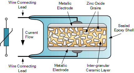
- The Metal Oxide Varistor is a voltage dependant resistor in which the resistance material is a metallic oxide, primarily zinc oxide (ZnO) pressed into a ceramic like material.
- It consists of approximately 90% zinc oxide as a ceramic base material plus other filler materials for the formation of junctions between the zinc oxide grains.
- Metal oxide varistor are now the most common type of voltage clamping device and are available for use at a wide range of voltages and currents.
- The use of a metallic oxide within their construction means that MOV’s are extremely effective in absorbing short- term voltage transients and have higher energy handling capabilities.
- As with the normal varistor, the metal oxide varistor starts conduction at a specific voltage and stops conduction when the voltage falls below a threshold voltage.
- The main differences between a standard silicon carbide (SiC) varistor and a MOV type varistor is that the leakage current through the MOV’s zinc oxide material is very small current at normal operating conditions and its speed of operation in clamping transients is much faster.
Construction:
The construction of a typical metal oxide varistor is as shown:
- To select the correct MOV for a particular application, it is desirable to have some knowledge of the source impedance and the possible pulse power of the transients
- However, metal oxide varistors are available in a wide range of varistor voltages, from about 10 volts to over 1,000 volts AC or DC, so selection can be helped by knowing the supply voltage.
- For example, selecting a MOV or silicon varistor for that matter, for voltage, its maximum continuous rms voltage rating should be just above the highest expected supply voltage, say 130 volts rms for a 120 volt supply, and 260 volts rms for a 230 volt supply.
- The maximum surge current value that a varistor will take depends on the transient pulse width and the number of pulse repetitions.
- If the peak pulse current rating is insufficient, then the varistor may overheat and become damaged. So for a varistor to operate without any failure or degradation, it must be able to quickly dissipate the absorbed energy of the transient pulse and return safely to its pre-pulse condition.
Q15) The separately excited dc motor in the figure below has a rated armature current of 20 A and a rated armature voltage of 150 V. An ideal chopper switching at 5 kHz is used to control the armature voltage. If La = 0.1 mH, Ra 1 , neglecting armature reaction, the duty ratio of the chopper to obtain 50% of the rated torque at the rated speed and the rated field current is?
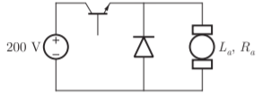
A15) Given the rated armature current

As rated armature voltage

Also, for the armature we have

And 
So , we get


 rated field current
At the rated conditions


For given torque

Therefore, chopper output=140 V


Q16) The Voltage Source Inverter (VSI) shown in the figure below is switched to provide a 50 Hz, square wave ac output voltage Vo across an RL load. Reference polarity of Vo and reference direction of the output current io are indicated in the figure. It is given that R = 3 ohms, L = 9.55 mH. (i) In the interval when V0 < 0 and i0 > 0 the pair of devices which conducts the load current is? (ii) Appropriate transition i.e., Zero Voltage Switching ZVS /Zero Current Switching ZCS of the IGBTs during turn-on/turn-off is?
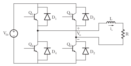
A16) (i) We consider the following two cases:
Case I: When Q Q1 2, ON In this case the +ve terminal of V0 will be at higher voltage. i.e. V0 > 0 and so i0 > 0 (i.e., it will be +ve). Now, when the Q1, Q2 goes to OFF condition we consider the second case.
Case II: When Q3, Q4 ON and Q, Q2 OFF: In this condition, -ve terminal of applied voltage V0 will be at higher potential i.e., V0 < 0 and since, inductor opposes the change in current so, although the polarity of voltage V0 is inversed, current remains same in inductor i.e. I0 > 0. This is the condition when conduction have been asked. In this condition (V0 > 0, I0>0), since, IGBT’s can’t conduct reverse currents therefore current will flow through D4 D3, until ID becomes negative. Thus, D3 and D4 conducts.
(ii) When Q4 Q3, is switched ON, initially due to the reverse current it remains in OFF state and current passes through diode. In this condition the voltage across Q3 and Q4 are zero as diodes conduct. Hence, it shows zero voltage switching during turn-ON.
Q17) In the 3-phase inverter circuit shown, the load is balanced and the gating scheme is 180c conduction mode. All the switching devices are ideal. (i) The rms value of load phase voltage is? (ii) If the dc bus voltage Vd = 300V the power consumed by 3-phase load is?
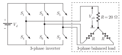
A17) For a three-phase bridge inverter, rms value of output line voltage is


(ii)

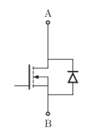
Q18) A three phase current source inverter used for the speed control of an induction motor is to be realized using MOSFET switches as shown below. Switches S1 to S6 are identical switches. The proper configuration for realizing switches S1 to S6 is?
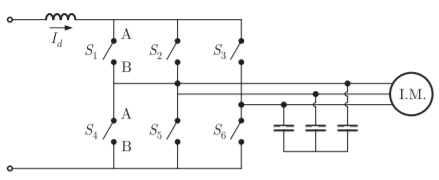
A18) The below figure allows bi direction power flow from source to the drive
Q19) The Current Source Inverter shown in figure is operated by alternately turning on thyristor pairs (T1, T2 ) and (T3 T4). If the load is purely resistive, the theoretical maximum output frequency obtainable will be?
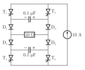
A19) In CSI let T3 and T4 already conducting at t = 0 At triggering T1 and T2, T3 and T4 are force cumulated. Again, at t= T/2, T1 and T2 are force cumulated. This completes a cycle.

Time constant = RC=4×0.5=2 sec
Frequency 
Q20) A single phase source inverter is feeding a purely inductive load as shown in the figure. The inverter is operated at 50 Hz in 1800 square wave mode. Assume that the load current does not have any dc component. The peak value of the inductor current i0 will be?
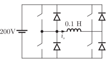
A20) Input is given as
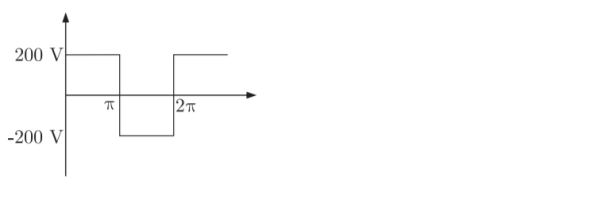
Here load current does not have any dc component
Peak current occur at (π/)


Q21) A three phase fully controlled bridge converter is feeding a load drawing a constant and ripple free load current of 10 A at a firing angle of 300. The approximate Total harmonic Distortion (%THD) and the rms value of fundamental component of input current will respectively be?
A21)
Total rms current 
Fundamental current 
THD=
Where 

Q22) A three-phase, fully controlled thyristor bridge converter is used as line commutated inverter to feed 50 kW power 420 V dc to a three-phase, 415 V(line), 50 Hz ac mains. Consider dc link current to be constant. The rms current of the thyristor is?
A22)
Given that 


RMS value of thyristor curent 
Q23) A three-phase, 440 V, 50 Hz ac mains fed thyristor bridge is feeding a 440 V dc, 15 kW, 1500 rpm separately excited dc motor with a ripple free continuous current in the dc link under all operating conditions, Neglecting the losses, the power factor of the ac mains at half the rated speed is?
A23) When losses are neglected

Here back emf with  is constant


At this firing angle


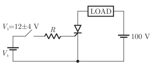
Q24) The triggering circuit of a thyristor is shown in figure. The thyristor requires a gate current of 10 mA, for guaranteed turn-on. The value of R required for the thyristor to turn on reliably under all conditions of Vb variation is?
A24)


Required value of 
Q25) The circuit in figure shows a full-wave rectifier. The input voltage is 230 V (rms) single-phase ac. The peak reverse voltage across the diodes D1 and D2 is
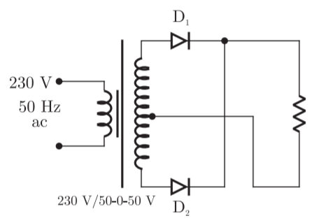
A25) Peak Inverse Voltage (PIV) across full wave rectifier is 2 


Q26) An ac induction motor is used for a speed control application. It is driven from an inverter with a constant V f / control. The motor name-plate details are as follows (no. Of poles = 2) VVf N :415 :3 :50 :2850 V V Hz rpm Ph The motor runs with the inverter output frequency set at 40 Hz, and with half the rated slip. The running speed of the motor is?
A26)


Where by (V/f) control

 new running speed of motor

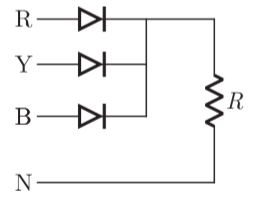
Q27) The circuit in figure shows a 3-phase half-wave rectifier. The source is a symmetrical, 3-phase four-wire system. The line-to-line voltage of the source is 100 V. The supply frequency is 400 Hz. The ripple frequency at the output is
A27)
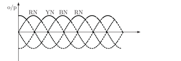
Ripple frequency =3f=3×400=1200 Hz
So from  ripple frequency =1200 Hz
Q28) An inverter has a periodic output voltage with the output wave form as shown in figure

When the conduction angle, a = 1200, the rms fundamental component of the output voltage is?
A28)
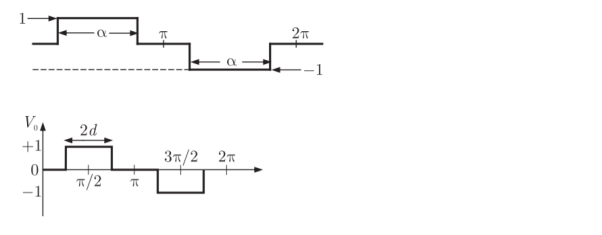
Output voltage
 RMS value of fundamental component


Q29) A variable speed drive rated for 1500 rpm, 40 Nm is reversing under no load. Figure shows the reversing torque and the speed during the transient. The moment of inertia of the drive is
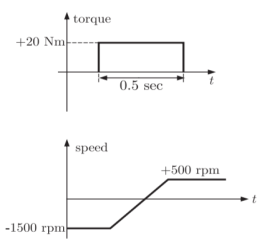
A29)


